EP0164723A2 - Appareil pour la régénération de signaux originaux - Google Patents
Appareil pour la régénération de signaux originaux Download PDFInfo
- Publication number
- EP0164723A2 EP0164723A2 EP85107145A EP85107145A EP0164723A2 EP 0164723 A2 EP0164723 A2 EP 0164723A2 EP 85107145 A EP85107145 A EP 85107145A EP 85107145 A EP85107145 A EP 85107145A EP 0164723 A2 EP0164723 A2 EP 0164723A2
- Authority
- EP
- European Patent Office
- Prior art keywords
- signal
- circuit
- output
- filter
- regenerating
- Prior art date
- Legal status (The legal status is an assumption and is not a legal conclusion. Google has not performed a legal analysis and makes no representation as to the accuracy of the status listed.)
- Withdrawn
Links
Images


Classifications
-
- G—PHYSICS
- G11—INFORMATION STORAGE
- G11B—INFORMATION STORAGE BASED ON RELATIVE MOVEMENT BETWEEN RECORD CARRIER AND TRANSDUCER
- G11B20/00—Signal processing not specific to the method of recording or reproducing; Circuits therefor
- G11B20/10—Digital recording or reproducing
-
- H—ELECTRICITY
- H03—ELECTRONIC CIRCUITRY
- H03K—PULSE TECHNIQUE
- H03K5/00—Manipulating of pulses not covered by one of the other main groups of this subclass
- H03K5/01—Shaping pulses
Definitions
- the present invention relates to an apparatus for regenerating original signals, and particularly to an apparatus for regenerating original signals while compensating missing portions that develop in the waveforms when digital signals are to be recorded, regenerated or transmitted.
- VTR video tape recorder
- the signals have to be transmitted or received via a transformer, resulting in a cut-off in the low-frequency band.
- the signals are transmitted and received via a circuit having resistance R and capacity C, such as a telephone circuit, the signal amplitude attenuates due to the transient phenomenon CR. Therefore, cut-off takes place not only in the low-frequency band but also in the high-frequency band as in the well as intermediate-frequency band.
- codes of the NRZ series develop conspicuous sag due to the cut-off of low frequencies, often making it difficult to distinguish "1" from "0".
- the quantized feedback method consists, as shown in Fig. l(a), of a decision circuit 12 made up of a comparator 2 and a latch circuit 3, a feedback circuit having a low-pass filter 4, and an adder 1. It is now presumed that an original signal g(t) generated from a signal source 20 passes through a system 21 which cuts off a predetermined frequency. This system may be, for instance, a recording/ regenerating system or a transmission system. It is presumed that this system has low-frequency cut-off characteristics P(f), and the signal which has passed through this system is regarded to be an input signal i(t).
- the fundamental operation of the quantized feedback method is to regenerate, from a signal 0(t) produced by the decision circuit 12 a signal s(t) of low-frequency component lost through the recording/regenerating system 21. That is, the decision circuit 12 consisting of comparator 2 and latch circuit 3 decided the output i(t) + s(t) of the adder 1 to be "1" or "0", and produces a signal 0(t) similar to the original signal g(t). The signal 0(t) is then passed through a low-pass filter 4 to extract the signal s(t) of a predetermined low-frequency component. If the filter 4 has transmission characteristics Q (f) as shown in Fig.
- the filter 4 regenerates output s(t) which corresponds to the original low-frequency component.
- the thus regenerated low-frequency signal s(t) is added to the input signal i(t) through the adder 1 to regenerate the signal 0(t) which is similar to the original signal g(t).
- Fig.2 shows signal waveforms at each of the above-mentioned portions.
- any error that occurs in the code may undergo chain propagation and may not be corrected.
- the reason is attributed to a positive feedback loop that is formed in the circuit by the comparator 2 and filter 4 as is obvious from the construction of Fib. l(a). Described below is the condition where error in the code undergoes chain propagation.
- amplitude of the signal produced by the adder 1 is standardized to 1.
- the present invention provides an apparatus which regenerates original signals by compensating waveforms of digital signals deteriorated in a system in which predetermined frequencies are cut off, without permitting code error to continue.
- the apparatus of the present invention comprises:
- the first circuit means is so constructed as to produce the third signal which corresponds to the signal i(t) + s(t) of Fig. 1 relying upon an open loop instead of a feedback loop, and can hence prevent code error from continuing.
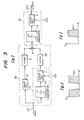
- Fig. 3 is a diagram showing the construction of an apparatus for regenerating original signals according to an embodiment of the present invention.
- Fig. 3(a) shows the construction in which the open loop is formed most simply, and which compensates the waveform without impairing the regeneration effect of the quantized feedback method.
- the apparatus consists of a first circuit means 30 and a second circuit means 12.
- the first circuit means 30 has a decision circuit 13 which converts the input signal i (t) into a binary signal, a filter 24 having cut-off characteristics similar to those of the aforementioned system 21 that cuts off predetermined frequencies, a delay circuit which delays the input signal i(t) by a time corresponding to the decision circuit 13, a filter 5 having characteristics complementary to the filter 24, and an adder 9.
- the decision circuit 13 consists of a comparator 10 and a latch circuit 11.
- the second circuit means 12 which works as a decision circuit consists of a comparator 2 and a latch circuit 3. Clock signals CLK are applied to the two latch circuits 3, 11.
- the input signal i(t) is allowed to pass through two paths. Nemely, the signal, on the one hand, passes through the decision circuit 13 consisting of comparator 10 and latch circuit 11, and through the filter 24, and passes, on the other hand, through the delay circuit 6 and the filter 5 having characteristics complementary to the filter 24. Outputs of these two filters 5, 24 are added together in the adder 9. The added output serves as an output signal of the first circuit means 30.
- the output signal contains noise and is hence converted into a binary signal through the decision circuit that consists of comparator 2 and latch circuit 3, in order to produce a signal 0(t) regenerated from the original signal.
- the filter 24 is constructed to have band-pass characteristics Q(f) shown in Fig. 3(c) to compensate for the above-mentioned characteristics, and the filter 5 is constructed to have characteristics P(f) shown in Fig. 3(b).
- a digital input signal i(t) is input, predetermined frequencies of the digital input signal i(t) being cut off.
- the decision circuit 13 converts the input signal i(t) into a binary signal "1" or "O".
- the signal is then sent to the band-pass filter 24 where predetermined frequency components are extracted.
- the delay circuit 6, on the other hand, delays the input signal i(t) by a time that corresponds to the decision circuit 13.
- the filter 5 allows the passage of only those frequency components of input signal i(t) that have a correlation to the filter 24. Outputs of the two filters 5, 24 are applied to the adder 9.
- Fig. 4 is a diagram showing the construction of-an apparatus for regenerating original signals according to another embodiment of the present invention.
- the apparatus consists of a first circuit means 30 and a second circuit means 12 like the apparatus of Fig. 3(a).
- the first circuit means 30 has a decision circuit 13 which converts the input signal i(t) into a binary signal, a delay circuit 6 which delays the input signal i(t) by a time that corresponds to the decision circuit 13, a subtracter 7 which finds a difference between the output of the decision circuit 13 and the output of the delay circuit 6, a filter 50 having characteristics complementary to those of the system 21 mentioned earlier that cuts off predetermined frequencies, a delay circuit 8 which delays the input signal i(t) for a period of time corresponding to the filter 50, and an adder 9 which adds the output of the filter 50 and the output of the delay circuit 8.
- the decision circuits 12, 13 are constituted by the comparators 2, 10 and latch circuits 3, 11, respectively, the latch circuits 3, 11 being served with clock signals CLK.
- the original signal is denoted by g(t) (not shown)
- a low-frequency signal is denoted by k(t) that is lost in the recording/regenerating system 21
- a remaining high-frequency signal is denoted by h(t).
- noise generated in the recording/regenerating system 21 is denoted by n(t)
- noise generated in the decision circuit 13 is denoted by n(t)
- noise generated in the decision circuit 13 is denoted by m(t).
- the signal produced by the decision circuit 13 is denoted by r(t) and the output of the subtracter 7 is denoted by d(t).
- the input signal i(t) is given by the following equiation,
- the decision circuit 13 regenerates a signal r(t) which is similar to the original signal g(t) and which is given by the following equation,
- the noise m(t) generates mainly from jitter components contained in the clock signals CLK, and wherein n(t)»m(t).
- the delay circuit 6 compensates the delay time generated by the decision circuit 13, and produces the signal i(t). Therefore, a differential signal d(t) of the subtracter 7 is given by,
- the differential signal d(t) is allowed to pass through the low-pass filter 50. Even when the signal after having been decided contains code error, the low-pass filter 50 limits the band thereof, so that the code error will not be generated in the final decision circuit 13 which is made up of comparator 10 and latch circuit 11. As will be explained later, the band of the filter 50 should be set to a minimum range that permits the passage of low-frequency signal t(t). If the signals and noise whose bands are limited by the filter 50 are denoted by de(t), ne(t) and me(t), the output de(t) is given by the following equation,
- the adder 9 regenerates the original signal a(t) on which noise is superposed.
- the signal a(t) is input to the decision circuit 12 which consists of comparator 2 and latch circuit 3, and is converted into a binary signal, in order to regenerate a signal 0(t) which is the same as the original signal g(t).
- the circuit of Fig. 4 does not have a feedback loop, either. Therefore, even if a code error develops in the decision circuit 13, the error is confined in this circuit only but is not propagated.
- a recording/regenerating system such as a VTR or the like has cut-off characteristics P(f) in a range of high frequencies. Therefore, there do not exist complete characteristics Q(f) that satisfy the conditions of equation (1). Hence, an approximation must be employed. Further, the cut-off characteristics P(f) vary depending upon the characteristics of the apparatus and recording conditions of the tape, and do not necessarily assume constant values. In general, it is quite difficult to change the characteristics Q(f) to cope with the change of characteristics P(f).
- the low-frequency component lost in the recording/regenerating system or in the transmission system can be automatically found from the output signal r(t) of the dicision circuit 13 and the input signal i(t), without at all being affected by the change in the low cut-off frequency characteristics.
- the embodiment of the invention improves all defects inherent in the quantized feedback method.
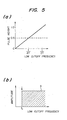
- Described below is a limit for improving code error caused by the cut off of low frequencies according to the embodiment. This is to find low cut-off frequencies in which code error generated in the decision circuit 13 of Fig. 4 also appears in the decision circuit 12. In general, the limit values of cut-off frequencies are also dependent upon the S/N ratio, and are difficult to delineate precisely.
- a limit value is represented by a cut-off frequency of the low-pass filter 50 at which a pulse which is generated by the decision circuit 13, which has a time width T and a crest value 1, reaches 1/2 level which is the decision level of the decision circuit 12 after having passed through the low-pass filter 50.
- the low cut-off frequency of the recording/regenerating system or the transmission system is equal to the cut-off frequency of the low-pass filter.
- Fig. 5(a) is a diagram showing the change in the crest value of pulse when the low cut-off frequency is changed
- Fig. 5(b) is a diagram showing ideal cut-off characteristics.
- Fig. 6 is a diagram which concretely illustrates the circuit of Fig. 4.
- the transmission rate of data is assumed to be 50 Mb/s.
- the input signal i(t) is input to a buffer amplifier 14, and an output therefrom is divided into two systems.
- the output on one system is input to a high-speed comparator 10 where it is converted into a binary signal, and is then converted through a latch circuit into a pulse train having a predetermined pulse width of 20 nS.
- the comparator 10 has a delay time of 2 to 3 nS
- the latch circuit 11 has a delay time which is one-half the period of 20 nS, i.e., has a delay time of 10 nS. Therefore, the total delay time is about 15 nS.
- the delay time is absorbed by an analog delay circuit 6 which is constituted by utilizing a coaxial cable.
- the coaxial cable has a delay time of about 4 to 5 nS/m.
- the low-pass filter 50 may be a Gaussian filter having flat group delay characteristics.
- the delay quantity varies depending upon the cut-off frequency and the degree. For instance, when the cut-off frequency is 10 MHz and the degree is third degree, the delay quantity will be about 100 nS. Therefore, the delay circuit 8 can be constituted by the coaxial cable having a length of 20 meters or more.
- Reference numeral 15 denotes a buffer amplifier
- 7 denotes a subtracter circuit
- 9 denotes an adder circuit.
- the operation time of the subtracter circuit 7 is selected to be nearly equal to the delay time of the buffer amplifier 15.
- the clock signal is applied to the latch circuit 11 and to the latch circuit 3 via delay circuit 16.
- the delay circuit 16 for the clock signal should have a variable range of one period, i.e., a variable range of 20 nS, and can be constituted by connecting gate circuits in a plurality of stages or can be constituted by using a delay line.
- a band-pass filter was used and in the embodiment of Fig. 4, a low-pass filter was used.
- a filter should be connected to compensate those portions that are lost in the recording/regenerating system or in the transmission system. Depending upon the cases, therefore, a high-pass filter may be used.
- waveforms that are deteriorated in the recording/regenerating system or in the transmitting system can be compensated to optimum values at all times without affected by the change in characteristics.
- chain phenomenon of code error that developed in the conventional quantized feedback method is now completely eliminated making it possible to stably regenerate original signals.
Landscapes
- Physics & Mathematics (AREA)
- Nonlinear Science (AREA)
- Engineering & Computer Science (AREA)
- Signal Processing (AREA)
- Signal Processing For Digital Recording And Reproducing (AREA)
- Dc Digital Transmission (AREA)
- Manipulation Of Pulses (AREA)
- Image Analysis (AREA)
- Investigating Or Analyzing Materials By The Use Of Magnetic Means (AREA)
Applications Claiming Priority (2)
| Application Number | Priority Date | Filing Date | Title |
|---|---|---|---|
| JP59119487A JPS60263512A (ja) | 1984-06-11 | 1984-06-11 | 波形補償方式 |
| JP119487/84 | 1984-06-11 |
Publications (2)
| Publication Number | Publication Date |
|---|---|
| EP0164723A2 true EP0164723A2 (fr) | 1985-12-18 |
| EP0164723A3 EP0164723A3 (fr) | 1988-09-07 |
Family
ID=14762484
Family Applications (1)
| Application Number | Title | Priority Date | Filing Date |
|---|---|---|---|
| EP85107145A Withdrawn EP0164723A3 (fr) | 1984-06-11 | 1985-06-11 | Appareil pour la régénération de signaux originaux |
Country Status (3)
| Country | Link |
|---|---|
| US (1) | US4682115A (fr) |
| EP (1) | EP0164723A3 (fr) |
| JP (1) | JPS60263512A (fr) |
Families Citing this family (2)
| Publication number | Priority date | Publication date | Assignee | Title |
|---|---|---|---|---|
| US4968898A (en) * | 1987-10-12 | 1990-11-06 | Jeol Ltd. | Pulse shaping circuit for radiation detector |
| JPH0575386A (ja) * | 1991-09-18 | 1993-03-26 | Fujitsu Ltd | 遅延回路 |
Family Cites Families (5)
| Publication number | Priority date | Publication date | Assignee | Title |
|---|---|---|---|---|
| DE1908247B2 (de) * | 1969-02-19 | 1971-03-04 | Fernseh Gmbh, 6100 Darmstadt | Schaltungsanordnung zur verringerung von stoerungen hoeherer frequenz (rauschen) in breitbandigen elektrischen signalen insbesondere fernsehsignalen |
| US3652872A (en) * | 1970-04-02 | 1972-03-28 | Us Air Force | Video bandwidth analyzer |
| US4238744A (en) * | 1977-09-08 | 1980-12-09 | Victor Company Of Japan, Ltd. | Frequency band dividing filter using delay-line filter |
| US4460871A (en) * | 1979-08-06 | 1984-07-17 | Orban Associates, Inc. | Multiband cross-coupled compressor with overshoot protection circuit |
| DE3132972A1 (de) * | 1981-08-20 | 1983-03-24 | Siemens AG, 1000 Berlin und 8000 München | Regenerator fuer digitale signale mit quantisierter rueckkopplung |
-
1984
- 1984-06-11 JP JP59119487A patent/JPS60263512A/ja active Granted
-
1985
- 1985-06-10 US US06/742,792 patent/US4682115A/en not_active Expired - Fee Related
- 1985-06-11 EP EP85107145A patent/EP0164723A3/fr not_active Withdrawn
Also Published As
| Publication number | Publication date |
|---|---|
| JPS60263512A (ja) | 1985-12-27 |
| JPH0562490B2 (fr) | 1993-09-08 |
| EP0164723A3 (fr) | 1988-09-07 |
| US4682115A (en) | 1987-07-21 |
Similar Documents
| Publication | Publication Date | Title |
|---|---|---|
| US3999129A (en) | Method and apparatus for error reduction in digital information transmission systems | |
| US9264264B2 (en) | Systems and methods for filtering a received signal to remove intersymbol interference | |
| US4122300A (en) | Data transmission system and application thereof to the transmission of analog signals and of data in a network with delta modulation | |
| KR910004426B1 (ko) | 맨체스터 코드 수신기 및 그 작동방법 | |
| US4367495A (en) | Method and apparatus for magnetic recording and reproduction of digital signal | |
| SE8503057D0 (sv) | Datamottagare for upptecknad data | |
| KR950004756A (ko) | 신호 처리 회로 | |
| US4805190A (en) | Detector logic circuit for a sychronous transmission system for data comprising ternary symbols and controlled partial response class 1, N=2 type intersymbol interference | |
| EP0304081B1 (fr) | Système de communication numérique utilisant les techniques de codage à réponse partielle et bipolaire | |
| US5005184A (en) | Method and apparatus for waveform equalization | |
| CA1191224A (fr) | Methode de suppression d'echos adaptative pour la transmission de signaux numeriques en duplex et appareil realisant cette methode | |
| KR890006084A (ko) | 디코더용 등화기 | |
| US4682115A (en) | Apparatus for regenerating original signals | |
| US4761797A (en) | Flexible regenerator | |
| CA1312936C (fr) | Methode d'extraction et de reglage de signaux d'horloge a reglage de phase par filtre a ondes acoustiques de surface | |
| JPH059975B2 (fr) | ||
| EP1098312B1 (fr) | Egalisateur de forme d'onde | |
| US3760111A (en) | Pulse regenerative repeater for a multilevel pulse communication system | |
| US4584696A (en) | Transmission response measurement | |
| KR100311488B1 (ko) | 적응성등화기 | |
| KR0178227B1 (ko) | 병렬 구조를 갖는 펄스 성형 필터 회로 | |
| JP2623638B2 (ja) | 復号装置 | |
| JP2978513B2 (ja) | 自動等化装置 | |
| SU1241520A1 (ru) | Регенератор цифрового сигнала | |
| Kanemasa et al. | An adaptive filter convergence method for echo cancellation and decision feedback equalization |
Legal Events
| Date | Code | Title | Description |
|---|---|---|---|
| PUAI | Public reference made under article 153(3) epc to a published international application that has entered the european phase |
Free format text: ORIGINAL CODE: 0009012 |
|
| 17P | Request for examination filed |
Effective date: 19850611 |
|
| AK | Designated contracting states |
Designated state(s): DE FR GB |
|
| PUAL | Search report despatched |
Free format text: ORIGINAL CODE: 0009013 |
|
| AK | Designated contracting states |
Kind code of ref document: A3 Designated state(s): DE FR GB |
|
| 17Q | First examination report despatched |
Effective date: 19900607 |
|
| STAA | Information on the status of an ep patent application or granted ep patent |
Free format text: STATUS: THE APPLICATION HAS BEEN WITHDRAWN |
|
| 18W | Application withdrawn |
Withdrawal date: 19920326 |
|
| RIN1 | Information on inventor provided before grant (corrected) |
Inventor name: MICHIKAWA, YUICHI Inventor name: ROKUDA, MORITO Inventor name: KATAYAMA, HITOSHI Inventor name: DOI, NOBUKAZU Inventor name: MITA, SEIICHI Inventor name: TAKAGI, HITOSHI Inventor name: SHIONO, HIROSHI Inventor name: IZUMITA, MORISHI |