EP0164921A2 - Plaquettes à circuit imprimé et méthode de fabrication de celles-ci - Google Patents
Plaquettes à circuit imprimé et méthode de fabrication de celles-ci Download PDFInfo
- Publication number
- EP0164921A2 EP0164921A2 EP85303436A EP85303436A EP0164921A2 EP 0164921 A2 EP0164921 A2 EP 0164921A2 EP 85303436 A EP85303436 A EP 85303436A EP 85303436 A EP85303436 A EP 85303436A EP 0164921 A2 EP0164921 A2 EP 0164921A2
- Authority
- EP
- European Patent Office
- Prior art keywords
- conductive
- layer
- metal
- medium
- electrically
- Prior art date
- Legal status (The legal status is an assumption and is not a legal conclusion. Google has not performed a legal analysis and makes no representation as to the accuracy of the status listed.)
- Withdrawn
Links
- 239000000758 substrate Substances 0.000 claims abstract description 29
- 229910052751 metal Inorganic materials 0.000 claims abstract description 18
- 239000002184 metal Substances 0.000 claims abstract description 17
- 239000012530 fluid Substances 0.000 claims abstract description 16
- 239000007787 solid Substances 0.000 claims abstract description 12
- 238000001035 drying Methods 0.000 claims abstract 7
- 239000010410 layer Substances 0.000 claims description 98
- 239000002966 varnish Substances 0.000 claims description 16
- 238000004519 manufacturing process Methods 0.000 claims description 9
- 239000002356 single layer Substances 0.000 claims description 8
- 239000004020 conductor Substances 0.000 claims description 7
- 238000000034 method Methods 0.000 claims description 6
- 239000004033 plastic Substances 0.000 claims description 5
- 229920003023 plastic Polymers 0.000 claims description 5
- 239000004332 silver Substances 0.000 claims description 5
- 229910052709 silver Inorganic materials 0.000 claims description 5
- 239000002245 particle Substances 0.000 claims description 3
- 239000000203 mixture Substances 0.000 claims description 2
- 239000012255 powdered metal Substances 0.000 claims 2
- RYGMFSIKBFXOCR-UHFFFAOYSA-N Copper Chemical compound [Cu] RYGMFSIKBFXOCR-UHFFFAOYSA-N 0.000 description 9
- 239000010949 copper Substances 0.000 description 9
- 229910052802 copper Inorganic materials 0.000 description 9
- 238000009413 insulation Methods 0.000 description 6
- PCHJSUWPFVWCPO-UHFFFAOYSA-N gold Chemical compound [Au] PCHJSUWPFVWCPO-UHFFFAOYSA-N 0.000 description 4
- 239000010931 gold Substances 0.000 description 4
- 229910052737 gold Inorganic materials 0.000 description 4
- PNEYBMLMFCGWSK-UHFFFAOYSA-N Alumina Chemical compound [O-2].[O-2].[O-2].[Al+3].[Al+3] PNEYBMLMFCGWSK-UHFFFAOYSA-N 0.000 description 3
- 239000004411 aluminium Substances 0.000 description 3
- 229910052782 aluminium Inorganic materials 0.000 description 3
- XAGFODPZIPBFFR-UHFFFAOYSA-N aluminium Chemical compound [Al] XAGFODPZIPBFFR-UHFFFAOYSA-N 0.000 description 3
- BQCADISMDOOEFD-UHFFFAOYSA-N Silver Chemical compound [Ag] BQCADISMDOOEFD-UHFFFAOYSA-N 0.000 description 2
- 238000005553 drilling Methods 0.000 description 2
- 239000011521 glass Substances 0.000 description 2
- 239000000463 material Substances 0.000 description 2
- 238000005476 soldering Methods 0.000 description 2
- QTBSBXVTEAMEQO-UHFFFAOYSA-M Acetate Chemical compound CC([O-])=O QTBSBXVTEAMEQO-UHFFFAOYSA-M 0.000 description 1
- 229910021578 Iron(III) chloride Inorganic materials 0.000 description 1
- 229910001209 Low-carbon steel Inorganic materials 0.000 description 1
- 230000015572 biosynthetic process Effects 0.000 description 1
- 238000005530 etching Methods 0.000 description 1
- 239000004744 fabric Substances 0.000 description 1
- RBTARNINKXHZNM-UHFFFAOYSA-K iron trichloride Chemical compound Cl[Fe](Cl)Cl RBTARNINKXHZNM-UHFFFAOYSA-K 0.000 description 1
- 239000012811 non-conductive material Substances 0.000 description 1
- 238000005096 rolling process Methods 0.000 description 1
- 239000000126 substance Substances 0.000 description 1
- 239000002344 surface layer Substances 0.000 description 1
Images


Classifications
-
- H—ELECTRICITY
- H05—ELECTRIC TECHNIQUES NOT OTHERWISE PROVIDED FOR
- H05K—PRINTED CIRCUITS; CASINGS OR CONSTRUCTIONAL DETAILS OF ELECTRIC APPARATUS; MANUFACTURE OF ASSEMBLAGES OF ELECTRICAL COMPONENTS
- H05K3/00—Apparatus or processes for manufacturing printed circuits
- H05K3/10—Apparatus or processes for manufacturing printed circuits in which conductive material is applied to the insulating support in such a manner as to form the desired conductive pattern
- H05K3/12—Apparatus or processes for manufacturing printed circuits in which conductive material is applied to the insulating support in such a manner as to form the desired conductive pattern using thick film techniques, e.g. printing techniques to apply the conductive material or similar techniques for applying conductive paste or ink patterns
- H05K3/1275—Apparatus or processes for manufacturing printed circuits in which conductive material is applied to the insulating support in such a manner as to form the desired conductive pattern using thick film techniques, e.g. printing techniques to apply the conductive material or similar techniques for applying conductive paste or ink patterns by other printing techniques, e.g. letterpress printing, intaglio printing, lithographic printing, offset printing
-
- H—ELECTRICITY
- H05—ELECTRIC TECHNIQUES NOT OTHERWISE PROVIDED FOR
- H05K—PRINTED CIRCUITS; CASINGS OR CONSTRUCTIONAL DETAILS OF ELECTRIC APPARATUS; MANUFACTURE OF ASSEMBLAGES OF ELECTRICAL COMPONENTS
- H05K3/00—Apparatus or processes for manufacturing printed circuits
- H05K3/46—Manufacturing multilayer circuits
- H05K3/4644—Manufacturing multilayer circuits by building the multilayer layer by layer, i.e. build-up multilayer circuits
- H05K3/4664—Adding a circuit layer by thick film methods, e.g. printing techniques or by other techniques for making conductive patterns by using pastes, inks or powders
-
- H—ELECTRICITY
- H05—ELECTRIC TECHNIQUES NOT OTHERWISE PROVIDED FOR
- H05K—PRINTED CIRCUITS; CASINGS OR CONSTRUCTIONAL DETAILS OF ELECTRIC APPARATUS; MANUFACTURE OF ASSEMBLAGES OF ELECTRICAL COMPONENTS
- H05K1/00—Printed circuits
- H05K1/02—Details
- H05K1/0286—Programmable, customizable or modifiable circuits
- H05K1/0287—Programmable, customizable or modifiable circuits having an universal lay-out, e.g. pad or land grid patterns or mesh patterns
- H05K1/0289—Programmable, customizable or modifiable circuits having an universal lay-out, e.g. pad or land grid patterns or mesh patterns having a matrix lay-out, i.e. having selectively interconnectable sets of X-conductors and Y-conductors in different planes
-
- H—ELECTRICITY
- H05—ELECTRIC TECHNIQUES NOT OTHERWISE PROVIDED FOR
- H05K—PRINTED CIRCUITS; CASINGS OR CONSTRUCTIONAL DETAILS OF ELECTRIC APPARATUS; MANUFACTURE OF ASSEMBLAGES OF ELECTRICAL COMPONENTS
- H05K1/00—Printed circuits
- H05K1/02—Details
- H05K1/03—Use of materials for the substrate
- H05K1/05—Insulated conductive substrates, e.g. insulated metal substrate
-
- H—ELECTRICITY
- H05—ELECTRIC TECHNIQUES NOT OTHERWISE PROVIDED FOR
- H05K—PRINTED CIRCUITS; CASINGS OR CONSTRUCTIONAL DETAILS OF ELECTRIC APPARATUS; MANUFACTURE OF ASSEMBLAGES OF ELECTRICAL COMPONENTS
- H05K1/00—Printed circuits
- H05K1/02—Details
- H05K1/09—Use of materials for the conductive, e.g. metallic pattern
- H05K1/092—Dispersed materials, e.g. conductive pastes or inks
- H05K1/095—Dispersed materials, e.g. conductive pastes or inks for polymer thick films, i.e. having a permanent organic polymeric binder
-
- H—ELECTRICITY
- H05—ELECTRIC TECHNIQUES NOT OTHERWISE PROVIDED FOR
- H05K—PRINTED CIRCUITS; CASINGS OR CONSTRUCTIONAL DETAILS OF ELECTRIC APPARATUS; MANUFACTURE OF ASSEMBLAGES OF ELECTRICAL COMPONENTS
- H05K2203/00—Indexing scheme relating to apparatus or processes for manufacturing printed circuits covered by H05K3/00
- H05K2203/01—Tools for processing; Objects used during processing
- H05K2203/0104—Tools for processing; Objects used during processing for patterning or coating
- H05K2203/0143—Using a roller; Specific shape thereof; Providing locally adhesive portions thereon
-
- H—ELECTRICITY
- H05—ELECTRIC TECHNIQUES NOT OTHERWISE PROVIDED FOR
- H05K—PRINTED CIRCUITS; CASINGS OR CONSTRUCTIONAL DETAILS OF ELECTRIC APPARATUS; MANUFACTURE OF ASSEMBLAGES OF ELECTRICAL COMPONENTS
- H05K2203/00—Indexing scheme relating to apparatus or processes for manufacturing printed circuits covered by H05K3/00
- H05K2203/05—Patterning and lithography; Masks; Details of resist
- H05K2203/0502—Patterning and lithography
- H05K2203/0534—Offset printing, i.e. transfer of a pattern from a carrier onto the substrate by using an intermediate member
-
- H—ELECTRICITY
- H05—ELECTRIC TECHNIQUES NOT OTHERWISE PROVIDED FOR
- H05K—PRINTED CIRCUITS; CASINGS OR CONSTRUCTIONAL DETAILS OF ELECTRIC APPARATUS; MANUFACTURE OF ASSEMBLAGES OF ELECTRICAL COMPONENTS
- H05K3/00—Apparatus or processes for manufacturing printed circuits
- H05K3/10—Apparatus or processes for manufacturing printed circuits in which conductive material is applied to the insulating support in such a manner as to form the desired conductive pattern
- H05K3/20—Apparatus or processes for manufacturing printed circuits in which conductive material is applied to the insulating support in such a manner as to form the desired conductive pattern by affixing prefabricated conductor pattern
- H05K3/207—Apparatus or processes for manufacturing printed circuits in which conductive material is applied to the insulating support in such a manner as to form the desired conductive pattern by affixing prefabricated conductor pattern using a prefabricated paste pattern, ink pattern or powder pattern
Definitions
- the present invention is concerned with printed circuit boards and their manufacture.
- Known types of single layer printed circuit board comprise an electrically non-conducting substrate onto which is fixed an electrically conducting medium, such as copper, in the form of a pattern defining a circuit configuration. Holes are drilled through the copper and substrate to allow the circuit components to be fixed thereto, for example by means of soldering.
- the substrate initially has one side covered with copper.
- an etchant-resistant medium such as an ink
- an etchant such as ferric chloride
- Known multi-layer printed circuit boards are made in the same way, except that a plurality of boards are placed one above the other and have holes in the same location on each board for fixing circuit components and for connecting each board together electrically, for example by means of soldering.
- a single layer printed circuit board comprising a non-conducting substrate onto which is printed a layer of conducting medium in the shape of a predetermined circuit configuration.
- a method of manufacturing I a single-layer printed circuit board comprising printing a layer of conducting medium onto a non-conducting substrate, said conducting medium being in the shape of a predetermined circuit configuration.
- a multi-layer printed circuit board comprising a non-conducting substrate onto which is printed a conducting medium and a non-conducting medium alternately in layers, there being at least two conducting layers and at least one non-conducting layer, said at least two conducting layers being in the shape of predetermined circuit configurations, and said at least one conducting layer having openings therein to allow access between the conducting layers in a predetermined manner.
- a method of manufacturing a multi-layer printed circuit board comprising printing a conducting medium alternately in layers onto a non-conducting substrate, there being at least two conducting layers and at least one non-conducting layer, said at least two conducting layers being in the shape of predetermined circuit configurations and said at least one non-conducting layer having openings therein to allow access between the conducting layers in a predetermined manner.
- the conducting medium is in the form of a metal based fluid, for example based on copper, silver, gold, aluminium or other conductive materials.
- the fluid is chosen so that at. least part of the fluid evaporates, leaving behind a solid metallic residue.
- the non-conducting layers of the multi-layer circuit board can be in the form of a commercially available non-conducting varnish or a combination of - varnish.and other electrically non-conducting materials.
- the multi-layer printed circuit board of the present invention it is possible to connect circuit components onto different conduction layers. This allows a reduction in the size of the board required.
- An advantage of the present invention over known types of printed circuit board is that no etching of the conducting medium is required. This considerably simplifies their manufacture and makes them cheaper to make.
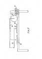
- a multi-layer board 10 has a substrate 12.
- Substrate 12 can be a layer of an electrically non-conductive material, such as a non-conductive board as used for conventional printed circuit boards.
- the substrate can be made of an electrically conductive material, for example a convenient metal.
- the copper surface of the substrate 12 is rendered electrically aon-conductive by the application thereto of an electrically non-conductive insulation layer 14, for example a suitable varnish.
- the substrate can in some circumstances be formed of a solid layer of an electrically conductive material, such as gold, which serves to carry power to the circuit components.
- the substrate should preferably be a good conductor of heat to dissipate the heat generated in the circuit.
- the substrate can thus be formed from a wide variety of materials, for example aluminium, mild steel, cloth, acetate film, glass paper and plasticised paper.
- a conducting track layer 16 represents a pattern of a predetermined circuit configuration.
- Layer 16 is printed onto the insulation layer 14, or directly onto the substrate 12 if the latter is non-conductive, in a manner described further hereinafter.
- the conducting medium used for track layer 16 is a fluid based on a metal such as copper, silver, gold or aluminium, part of which evaporates to leave a conductive metallic circuit on the insulated substrate 12.
- the connections that are required between conducting layer 16 and subsequent conducting layers are made via openings 20 in the layer of varnish 18. These openings 20 then form contact points for such connections.
- Such openings 20 may also be used for connecting circuit components to various conducting layers.
- Fig.l shows a further conducting track layer 22 printed onto the layer of varnish 18 to complete the circuit configuration.
- any number of conducting layers and non-conducting layers may be sandwiched together.
- components such as indicated by reference numeral 24 are fixed onto the conducting layers on the board.
- a further insulation layer 26 can be applied over the track layer 22 when necessary.
- Conventional components 24 may be used, but this requires drilling through the board.
- surface mounted components may be used which stick directly onto the top layer 22 (or 26), thus obviating the need for drilling.
- Fig.2 illustrates how tracks on three different conductive layers might be interconnected with components to complete the circuit on the board.
- the substrate 12 and the first conducting track layer 16 are essential, although non-conducting insulation layers corresponding to layers 14 and 18 can be included where appropriate.
- resistors can be incorporated into the conductive track layer thus saving space on the outer parts of the board.
- a reduction in the required board size over conventional boards is also achieved because components are able to connect to different layers and it is, therefore, not necessary to have all the contact points on the surface layer.
- the technique comprises taking a photographic negative of the required circuit configuration. From this a plastics printing plate 30 is produced wherein the pattern of the circuit is in slight relief from the rest of the surface of the plate.
- the conducting medium containing the metallic element is then applied from rubber rollers 32 to the plate 30 by displacing the rollers 32 over the plate 30 as indicated by the chain line 34 in Fig.3.
- the image is then transferred to a cylinder 36 which is covered in a rubber sheet or blanket 38 by rolling the cylinder over the plate 30 as indicated by solid line 40 in Fig.3.
- the rubber picks up a perfect image from the printing plate 30 and transfers this to the substrate 42 (corresponding, for example, to substrate 12 or insulation layer 14 of Fig.l).
- the conducting medium is then dried.
- a plastics plate can be produced in a similar manner for each non-conducting layer and for each subsequent conducting layer.
- the layer of varnish is similarly printed over the dry conducting layer on the substrate.
- Subsequent conducting layers and non-conducting layers are then applied to the board in the same manner until the circuit board is completed. Suitable varnishes are presently available commercially. '
- the conducting medium itself can be a mixture of silver and two separate varnishes.
- the latter varnishes are selected such that, when the conducting medium is dried by the application of heat, one varnish evaporates and the other oxidises and binds the flaked and/or powdered particles of silver into a solid layer.
- the non-conducting varnish may have to contain powdered glass or such substance, and after the final application the board would be heated until the varnish material sintered or melted into a glazed surface.
- An alternative layer arrangement for the board is as follows.
- a suitable non-conductive substrate is chosen, such as aluminium oxide, and a conductive layer is then put down on top of this substrate, the conductive layer being a relatively thick, solid layer of a metal such as gold, which can then be used to carry power (as compared to low energy signals) to operate all components.
- Non-conductive and conductive track layers are then applied to this solid conductive layer as before.
- the conductive tracks are used only for carrying signals which require low power. The tracks can therefore then be of minimum width and thickness.
- circuitry to be applied directly to the body or housing of an item of equipment to be controlled.
- the circuitry can be printed directly onto the plastics body so that the body itself serves as the substrate 12. It is then no longer necessary to provide a separate substrate, the electronic components being mounted directly onto the body or other housing part onto which the basic circuit has been printed.
Landscapes
- Engineering & Computer Science (AREA)
- Manufacturing & Machinery (AREA)
- Microelectronics & Electronic Packaging (AREA)
- Production Of Multi-Layered Print Wiring Board (AREA)
- Insulated Metal Substrates For Printed Circuits (AREA)
Applications Claiming Priority (2)
| Application Number | Priority Date | Filing Date | Title |
|---|---|---|---|
| GB8412606A GB8412606D0 (en) | 1984-05-17 | 1984-05-17 | Printed circuit boards |
| GB8412606 | 1984-05-17 |
Publications (2)
| Publication Number | Publication Date |
|---|---|
| EP0164921A2 true EP0164921A2 (fr) | 1985-12-18 |
| EP0164921A3 EP0164921A3 (fr) | 1987-06-03 |
Family
ID=10561099
Family Applications (1)
| Application Number | Title | Priority Date | Filing Date |
|---|---|---|---|
| EP85303436A Withdrawn EP0164921A3 (fr) | 1984-05-17 | 1985-05-16 | Plaquettes à circuit imprimé et méthode de fabrication de celles-ci |
Country Status (2)
| Country | Link |
|---|---|
| EP (1) | EP0164921A3 (fr) |
| GB (1) | GB8412606D0 (fr) |
Cited By (11)
| Publication number | Priority date | Publication date | Assignee | Title |
|---|---|---|---|---|
| FR2614168A1 (fr) * | 1987-04-15 | 1988-10-21 | Toshiba Kk | Dispositif a circuits electroniques multicouches et son procede de fabrication |
| US4829405A (en) * | 1988-03-14 | 1989-05-09 | International Business Machines Corporation | Tape automated bonding package |
| US4933810A (en) * | 1987-04-30 | 1990-06-12 | Honeywell Inc. | Integrated circuit interconnector |
| WO1990007858A3 (fr) * | 1988-12-24 | 1990-08-09 | Technology Applic Co Ltd | Procede ameliore de fabrication de circuits imprimes |
| EP0299221A3 (en) * | 1987-07-13 | 1990-11-07 | International Business Machines Corporation | Printed circuit panel |
| EP0335281A3 (fr) * | 1988-03-28 | 1990-12-27 | Kaleto Ag | Procédé de fabrication de circuits imprimés adaptés à l'utilisateur |
| WO1991006118A1 (fr) * | 1989-10-20 | 1991-05-02 | E.I. Du Pont De Nemours And Company | Procede non photographique de configuration de films de polymeres organiques |
| WO1994005139A1 (fr) * | 1992-08-17 | 1994-03-03 | Robert Bosch Gmbh | Procede de production de couches electroconductrices finement structurees |
| US5314788A (en) * | 1986-01-24 | 1994-05-24 | Canon Kabushiki Kaisha | Matrix printed board and process of forming the same |
| CH698612B1 (de) * | 2006-12-21 | 2009-09-15 | Microdul Ag | Elektronische Schaltungsanordnung mit wenigstens einem elektronischen Bauelement sowie ein Verfahren zum Herstellen einer solchen Schaltungsanordnung. |
| AT510079A1 (de) * | 2010-06-04 | 2012-01-15 | Prelonic Technologies Gmbh | Verfahren zur herstellung von mehrschichtigen schaltungen und mehrschichtige schaltung |
Family Cites Families (4)
| Publication number | Priority date | Publication date | Assignee | Title |
|---|---|---|---|---|
| FR2437427A1 (fr) * | 1978-09-08 | 1980-04-25 | Labo Electronique Physique | Encre serigraphiable, a cuire sous atmosphere non oxydante |
| DE3225483A1 (de) * | 1981-11-17 | 1983-05-26 | Robert Bosch Gmbh, 7000 Stuttgart | Verfahren zur herstellung elektrisch leitfaehiger bereiche |
| FR2524706A1 (fr) * | 1982-04-01 | 1983-10-07 | Cit Alcatel | Procede d'elaboration de circuits d'interconnexion multicouches |
| US4564563A (en) * | 1983-09-30 | 1986-01-14 | Electro Materials Corp. Of America | Solderable conductor |
-
1984
- 1984-05-17 GB GB8412606A patent/GB8412606D0/en active Pending
-
1985
- 1985-05-16 EP EP85303436A patent/EP0164921A3/fr not_active Withdrawn
Cited By (11)
| Publication number | Priority date | Publication date | Assignee | Title |
|---|---|---|---|---|
| US5314788A (en) * | 1986-01-24 | 1994-05-24 | Canon Kabushiki Kaisha | Matrix printed board and process of forming the same |
| FR2614168A1 (fr) * | 1987-04-15 | 1988-10-21 | Toshiba Kk | Dispositif a circuits electroniques multicouches et son procede de fabrication |
| US4933810A (en) * | 1987-04-30 | 1990-06-12 | Honeywell Inc. | Integrated circuit interconnector |
| EP0299221A3 (en) * | 1987-07-13 | 1990-11-07 | International Business Machines Corporation | Printed circuit panel |
| US4829405A (en) * | 1988-03-14 | 1989-05-09 | International Business Machines Corporation | Tape automated bonding package |
| EP0335281A3 (fr) * | 1988-03-28 | 1990-12-27 | Kaleto Ag | Procédé de fabrication de circuits imprimés adaptés à l'utilisateur |
| WO1990007858A3 (fr) * | 1988-12-24 | 1990-08-09 | Technology Applic Co Ltd | Procede ameliore de fabrication de circuits imprimes |
| WO1991006118A1 (fr) * | 1989-10-20 | 1991-05-02 | E.I. Du Pont De Nemours And Company | Procede non photographique de configuration de films de polymeres organiques |
| WO1994005139A1 (fr) * | 1992-08-17 | 1994-03-03 | Robert Bosch Gmbh | Procede de production de couches electroconductrices finement structurees |
| CH698612B1 (de) * | 2006-12-21 | 2009-09-15 | Microdul Ag | Elektronische Schaltungsanordnung mit wenigstens einem elektronischen Bauelement sowie ein Verfahren zum Herstellen einer solchen Schaltungsanordnung. |
| AT510079A1 (de) * | 2010-06-04 | 2012-01-15 | Prelonic Technologies Gmbh | Verfahren zur herstellung von mehrschichtigen schaltungen und mehrschichtige schaltung |
Also Published As
| Publication number | Publication date |
|---|---|
| GB8412606D0 (en) | 1984-06-20 |
| EP0164921A3 (fr) | 1987-06-03 |
Similar Documents
| Publication | Publication Date | Title |
|---|---|---|
| ES8607673A1 (es) | Procedimiento para fabricar placas conductoras flexibles con contactos de paso para elevados esfuerzos por flexion | |
| EP0164921A2 (fr) | Plaquettes à circuit imprimé et méthode de fabrication de celles-ci | |
| US5079065A (en) | Printed-circuit substrate and method of making thereof | |
| EP0167344A3 (fr) | Circuit multicouche interconnecté utilisant un diélectrique photosensible | |
| EP0101791A3 (fr) | Circuit à plusieurs couches | |
| EP0170477A3 (fr) | Systèmes multicouche et procédé de fabrication | |
| EP0929208A3 (fr) | Assemblage de circuits flexibles chimiquement gravés ayant des couches conductrices multiples et son procédé de fabrication | |
| GB2033667A (en) | Improvements in circuit boards | |
| JP2712295B2 (ja) | 混成集積回路 | |
| US4762732A (en) | Process for forming silver conductors on a substrate | |
| JPS60117796A (ja) | 多層配線基板及びその製造方法 | |
| JPS5998597A (ja) | 多層プリント配線板 | |
| JPH02301187A (ja) | 両面配線基板の製造方法 | |
| WO2000046837A2 (fr) | Procede ameliore de fabrication de cartes de circuit imprime | |
| KR200199631Y1 (ko) | 다층 인쇄회로기판 | |
| WO2000059000A8 (fr) | Realisation de trous de passage segmentes dans des cartes a circuits integres | |
| JPS6228793Y2 (fr) | ||
| GB1386344A (en) | Manufacture of multiple laminated conductor boards | |
| GB2075270A (en) | Method for metalizing holes in insulating material | |
| JPS57193051A (en) | Multilayer circuit board | |
| JPS6347158B2 (fr) | ||
| JPS6296884U (fr) | ||
| JPH03185897A (ja) | 多層配線基板の製造方法 | |
| JPH08274416A (ja) | プリント配線板及びその製造方法 | |
| JPH0133959B2 (fr) |
Legal Events
| Date | Code | Title | Description |
|---|---|---|---|
| PUAI | Public reference made under article 153(3) epc to a published international application that has entered the european phase |
Free format text: ORIGINAL CODE: 0009012 |
|
| AK | Designated contracting states |
Designated state(s): AT BE CH DE FR GB IT LI LU NL SE |
|
| PUAL | Search report despatched |
Free format text: ORIGINAL CODE: 0009013 |
|
| AK | Designated contracting states |
Kind code of ref document: A3 Designated state(s): AT BE CH DE FR GB IT LI LU NL SE |
|
| 17P | Request for examination filed |
Effective date: 19871130 |
|
| STAA | Information on the status of an ep patent application or granted ep patent |
Free format text: STATUS: THE APPLICATION IS DEEMED TO BE WITHDRAWN |
|
| 18D | Application deemed to be withdrawn |
Effective date: 19891201 |