EP0165066A2 - FM-Signal-Demodulator - Google Patents
FM-Signal-Demodulator Download PDFInfo
- Publication number
- EP0165066A2 EP0165066A2 EP85304221A EP85304221A EP0165066A2 EP 0165066 A2 EP0165066 A2 EP 0165066A2 EP 85304221 A EP85304221 A EP 85304221A EP 85304221 A EP85304221 A EP 85304221A EP 0165066 A2 EP0165066 A2 EP 0165066A2
- Authority
- EP
- European Patent Office
- Prior art keywords
- signal
- signals
- producing
- frequency
- video signal
- Prior art date
- Legal status (The legal status is an assumption and is not a legal conclusion. Google has not performed a legal analysis and makes no representation as to the accuracy of the status listed.)
- Withdrawn
Links
Images


Classifications
-
- H—ELECTRICITY
- H03—ELECTRONIC CIRCUITRY
- H03D—DEMODULATION OR TRANSFERENCE OF MODULATION FROM ONE CARRIER TO ANOTHER
- H03D3/00—Demodulation of angle-, frequency- or phase- modulated oscillations
Definitions
- This invention relates to a demodulator for demodulating frequency-modulated (referred to as FM hereinafter) signals, and more particularly a demodulator for demodulating FM video signals reproduced from a magnetic recording medium in a magnetic recording and reproducing apparatus such as a video tape recorder.
- FM frequency-modulated
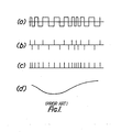
- a FM signal demodulating circuit demodulates the reproduced FM video signal by the so-called pulse counter method to obtain the original video signal.
- the reproduced FM video signal is passed in turn through a limiter to be such a rectangular pulse-train signal like a compressional wave as shown in Fig. l(a), through a differentiator to be a pulse-train signal as shown in Fig. l(b), where it is further full-wave rectified to be such a signal as shown in Fig. l(c), and finally through an integrator to be a demodulated signal which is substantially the original video signal as shown in Fig. l(d).
- This signal processing is explained in detail in "Video Recording Techniques" by Nobutoshi Kihara, published by Sanpo Shuppan, Japan.
- the carrier frequency of the FM video signal is very close to the higher side frequency of video signal of VTR, a part of the FM video signal, when demodulated, becomes a crosstalk appearing in the original video signal, resulting in fine streaks or beat appearing on the display screen.
- full-wave rectification is employed to double the carrier frequency, so that the crosstalk components of FM video signal in the original video signal are suppressed.
- Usual home VTRs operate under a condition in which video frequency band is 1.5 MHz, frequency deviation is 1.0 MHz, and carrier frequency is 3.9 MHz. Therefore, the first and second lower sidebands do not cause the crosstalk.
- the conventional FM signal demodulating circuit is used in a VTR requiring high resolution and high S/N, or having wide video transmission band and large frequency deviation or emphasis, the second and third lower sidebands appear in the video signal as the crosstalk signals, to cause deterioration of- picture quality.
- frequency deviation is doubled, so that powers of the second and third lower sidebands increase, resulting in production of fine streaks and beat, notably, deterioration of S/N at the edge of video signal.
- the FM signal demodulator comprises: phase shifting means having characteristics of constant wide frequency band and constant- group delay, for producing from a FM video signal two FM video signals which are different in phase by 90° from each other; and demodulating means for detecting phase information of the FM video signal from the two FM video signals from the phase shifting means wherein the FM video signal is demodulated after carrier frequency is at least quadrupled.
- the phase shifting means may comprises odd- and even-type transversal filter for producing the two FM video signals which are different in phase by 90° from each other.
- the two FM video signals are respectively doubled in carrier frequency by known means, and the frequency-doubled FM video signals are added to each other, thereby to be a frequency-quadrupled FM video signal.
- This frequency-quadrupled FM video signal is demodulated by known means such as an integrator to be a video signal which is substantially identical with the original video signal. By a proper combination of this arrangement, the carrier frequency can be further multiplied prior to demodulation.
- the carrier frequency is at least quadrupled prior to demodulation of FM video signal enables to demodulate the FM video signal without causing crosstalk of components of the FM video signal into the original video signal. Accordingly, this permits a VTR to have high resolution and SIN without producing fine streaks or beat on the screen, and wihtout deteriorating S/N at the edge of the video signal. Further, owing to the use of transversal filters to generate the two FM video signals having phases different by 90° from each other, the relative phase difference (90°) can be ensured to remain constant in the overall frequency band.
- the phase characteristic of each of the transversal filters is linear, which ensures a constant group delay without consequent group delay distortion.
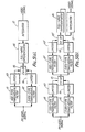
- reference characters 1 and 2 designate odd- and even-type transversal filters constituting a phase shifter, respectively.
- a FM video signal is inputted into odd- and even-type transversal filters 1 and 2, and at their outputs, constant group frequency-delayed FM video signals which are different in phase by 90° from each other in the whole frequency band are obtained.
- the two FM video signals are applied to limiters 3, 4 of the same construction, respectively, to become rectangular pulse-train signals as shown in Fig. l(a).
- Each of the limiter circuits 3, 4 can be comprised by a differential amplifier.
- the outputs of the limiters 3, 4 are inputted into full-wave differentiators 5, 6 which are identical in construction.
- Each of the full-wave differentiators 5, 6 is a known differentiator comprised by capacitors, resistors and an AND circuit. From the full wave differentiators 5, 6, pulse signals shown in Fig. l(c) whose carrier frequencies are doubled are outputted, and then inputted into an adder 7, which can be comprised by resistors.
- the construction elements of limiters 3, 4 and full-wave differentiators 5, 6 are the same as those of the conventional FM signal demodulating circuit. Since the carrier frequencies of the outputs of the full wave differentiators 5 and 6 are twice that of the input FM video signal, and the phases of them are different by 90° from each other, at an output terminal of the adder 7 is obtained a carrier frequency-quadrupled pulse signal. This signal is applied to an integrator 8.
- the integrator 8 which is a general low-pass filter, extracts the original video signal from the FM video signal. Such quadruplication of. carrier frequency enables to avoid crosstalks of components of FM video signal up to the third lower sideband. This is expressed by the following formula, assuming carrier frequency f c , video signal band f ab , frequency generated by the third lower sideband when the carrier frequency is quadrupled f 3w :
- Formula (3) is always established in usual VTRs. Accordingly it is possible to suppress components of FM signal up to the third lower sideband.
- Fig. 3(a) shows a transversal filter constructed by one delay element (delay T).
- An input signal f a inputted to an input terminal 12 is delayed by a time T by a delay element 9 to be a delayed signal f b .
- a factor +1 or -1 is added to the delayed signal f b by a factoring circuit 10.
- the factor is +1, the transversal filter becomes an even-type transversal filter, and when the factor is -1, the transversal filter becomes an odd-type transversal filter.
- the factor added signal from the factoring circuit 10 is added with the input signal f a by an adder 11 to be an output signal f 0 in the case of the even-type transversal filter or f 1 in the case of the odd-type transversal filter, which is outputted from an output terminal 13.
- This filtering process is expressed by a vector diagram shown in Fig. 3(b). As seen from Fig. 3 (b) the relative phase difference between the output signal f a of the even-type transversal filter and the output signal f b of the even-type transversal filter is always 90°.
- the second term represents frequency characteristic and the third term represents phase characteristic. These indicate they have linear phase characteristic and constant group delay. This means that the FM video signal does not undergo group delay distortion when passed through the transversal filters.
- the output f c at the T/2 delay tap 14 of the delay element 9 can be used in place of the output of the even-type transversal filter. This is expressed by the following equation:
- f 0 ( ⁇ ) and f c ( ⁇ ) are the same phase. Accordingly, the T/ 2 delay- tap output can be used instead of the output of the even-type transversal filter.
- the frequency characteristics are sinusoidal (sine and cosine wave, respectively). Taking the influence on video signal demodulated from FM video signal into consideration, it is preferable that the frequency characteristic is constant.
- multistage transversal filters may be used.
- Figs. 4(a) and (b) show examples of transversal filter having 5-stage delay elements, which enable the frequency characteristic in the frequency range of about 2 - 16 MHz to be constant.
- the transversal filter is constructed by delay elements 21-25 (delay time of each of them being T), a first group of factoring circuits 26-31, an adder 32 for adding outputs of the factoring circuits 26-31, a second group of factoring circuits 33-38, and an adder 39 for adding outputs of the factoring circuits 33-38.
- An output signal of the adder 32 is an output signal of an even-type transversal filter and is outputted from an even-type output terminal 13a.
- An output signal of the adder 39 is an output signal of an odd-type transversal filter and is outputted from an odd-type output terminal 13b.
- aT/2 delay tap 14 is provided.
- a signal obtained at the T/2 delay tap 14 is identical with the output signal of the even-type transversal filter.
- FIGs. 5(a) and (b) Other embodiments of FM signal demodulator of the invention are shown in Figs. 5(a) and (b). From the input FM video signal are obtained two rectangular pulse-train signals which are different in phase by 90° from each other by the combination of the odd-type transversal filter 61 and the limiter 63 and the combination of the even-type transversal filter 62 and the limiter 64, respectively.
- the two signals outputted from the limiters 63 and 64 are applied to an exclusive OR (EX-OR, hereafter) circuit 65 to be a pulse-train signal whose carrier frequency is doubled with respect to the carrier frequency of the input FM video.
- the EX-OR circuit 65 can be substituted by a coincident circuit.
- the output signal of the EX-OR circuit is rectified by a full-wave rectifier 66 so that a pulse-train signal having quadrupled carrier frequency is obtained at the output terminal of the full-wave rectifier 66.
- the frequency-quadrupled output signal of the full-wave rectifier 66 is applied to an integrator 67 to be demodulated to a video signal which is identical with the original video signal.
- the EX-OR circuit 65 is connected another frequency-doubling circuit constructed by transversal filters 61', 62', limiters 63', 64' and EX-OR circuit 65', which is identical with the frequency-doubling circuit constructed by transversal filters 61, 62, limiters 63, 64 and EX-OR circuit 65.
- the frequency of the output signal of the full-wave rectifier 66 is 8 times the carrier frequency of the input FM video signal.
- plural frequency-doubling circuits can be cascade connected to obtain a signal having a frequency which is 16, 32 or more times the carrier frequency of the input FM video signal.
- FM signal demodulator When the FM signal demodulator according to the invention is used, components of FM video signal up to the third lower sideband are suppressed; and thus the following condition is given: wherein f is carrier frequency and f ab is video signal band.
- FM video signal is set according to equations (3) and (7), then are obtained the frequency allocations shown in Figs. 6(a) and (b) with FM signal demodulator in accordance with the prior art and the invention, respectively.
- the diagrams indicate that the demodulator according to the invention enables setting the carrier frequency f c to a lower frequency compared with the prior art demodulator. This, taking the recording and reproducing characteristics of the system, including magnetic tape and magnetic head, particularly for VTR, into consideration, contributes to improvement in S/N of the reproduced video signal of VTR because the setting of carrier frequency f to lower band is associated with the use of better S/N portion.
- phase shifting means transversal filter
- the phase shifting means are separated into two blocks, i.e. even-type and odd-type transversal filters, for easier understanding of the invention.
- the signals corresponding to the output signals of the even- and odd-type transversal filters can be obtained from a single transversal filter construction.
- the extraction of the demodulated signal can be made by the conventional techniques or methods, such as the so-called FM signal demodulation method with delay line or quadrature detection method, PLL (phase locked loop) technique and TAN method (as exemplified in the Journal of Electronics and Communications Institute J67-B, No. 5, 1984).
Landscapes
- Engineering & Computer Science (AREA)
- Power Engineering (AREA)
- Television Signal Processing For Recording (AREA)
- Superheterodyne Receivers (AREA)
Applications Claiming Priority (8)
| Application Number | Priority Date | Filing Date | Title |
|---|---|---|---|
| JP123054/84 | 1984-06-15 | ||
| JP59123054A JPS612405A (ja) | 1984-06-15 | 1984-06-15 | Fm復調回路 |
| JP59127025A JPS618771A (ja) | 1984-06-20 | 1984-06-20 | 記録再生装置 |
| JP59127026A JPS615605A (ja) | 1984-06-20 | 1984-06-20 | Fm復調回路 |
| JP127025/84 | 1984-06-20 | ||
| JP127026/84 | 1984-06-20 | ||
| JP59262110A JPS61140287A (ja) | 1984-12-12 | 1984-12-12 | Fm復調回路 |
| JP262110/84 | 1984-12-12 |
Publications (2)
| Publication Number | Publication Date |
|---|---|
| EP0165066A2 true EP0165066A2 (de) | 1985-12-18 |
| EP0165066A3 EP0165066A3 (de) | 1987-05-20 |
Family
ID=27470905
Family Applications (1)
| Application Number | Title | Priority Date | Filing Date |
|---|---|---|---|
| EP85304221A Withdrawn EP0165066A3 (de) | 1984-06-15 | 1985-06-13 | FM-Signal-Demodulator |
Country Status (2)
| Country | Link |
|---|---|
| US (1) | US4629994A (de) |
| EP (1) | EP0165066A3 (de) |
Cited By (2)
| Publication number | Priority date | Publication date | Assignee | Title |
|---|---|---|---|---|
| EP0399758A3 (de) * | 1989-05-25 | 1992-03-25 | Sony Corporation | FM-Demodulator |
| EP1667346A4 (de) * | 2003-09-08 | 2008-01-23 | Nippon Telegraph & Telephone | OPTISCHER SIGNALEMPFûNGER, OPTISCHESIGNALEMPFANGSVORRICHTUNG UND OPTISCHES SIGNAL ERBTRAGUNGSSYSTEM |
Families Citing this family (3)
| Publication number | Priority date | Publication date | Assignee | Title |
|---|---|---|---|---|
| JPH01296704A (ja) * | 1988-05-24 | 1989-11-30 | Matsushita Electric Ind Co Ltd | Fm復調装置 |
| US5245461A (en) * | 1991-01-15 | 1993-09-14 | The Charles Stark Draper Laboratory | Analog optical FM receiver |
| US6385442B1 (en) * | 1998-03-04 | 2002-05-07 | Symbol Technologies, Inc. | Multiphase receiver and oscillator |
Family Cites Families (7)
| Publication number | Priority date | Publication date | Assignee | Title |
|---|---|---|---|---|
| US3764927A (en) * | 1971-12-07 | 1973-10-09 | Gen Datacomm Ind Inc | Wide band frequency discriminator |
| FR2170152B1 (de) * | 1972-02-03 | 1976-05-14 | Rca Corp | |
| GB1437325A (en) * | 1972-08-18 | 1976-05-26 | Rca Corp | Fm demodulator |
| US3971998A (en) * | 1975-05-02 | 1976-07-27 | Bell Telephone Laboratories, Incorporated | Recursive detector-oscillator circuit |
| US4238744A (en) * | 1977-09-08 | 1980-12-09 | Victor Company Of Japan, Ltd. | Frequency band dividing filter using delay-line filter |
| JPS5666907A (en) * | 1979-11-05 | 1981-06-05 | Sony Corp | Fm demodulator |
| US4412340A (en) * | 1981-12-28 | 1983-10-25 | The United States Of America As Represented By The Secretary Of The Army | One-bit autocorrelation envelope detector |
-
1985
- 1985-06-11 US US06/743,369 patent/US4629994A/en not_active Expired - Fee Related
- 1985-06-13 EP EP85304221A patent/EP0165066A3/de not_active Withdrawn
Cited By (3)
| Publication number | Priority date | Publication date | Assignee | Title |
|---|---|---|---|---|
| EP0399758A3 (de) * | 1989-05-25 | 1992-03-25 | Sony Corporation | FM-Demodulator |
| EP1667346A4 (de) * | 2003-09-08 | 2008-01-23 | Nippon Telegraph & Telephone | OPTISCHER SIGNALEMPFûNGER, OPTISCHESIGNALEMPFANGSVORRICHTUNG UND OPTISCHES SIGNAL ERBTRAGUNGSSYSTEM |
| US7444084B2 (en) | 2003-09-08 | 2008-10-28 | Nippon Telegraph And Telephone Corporation | Optical signal receiver, optical signal receiving equipment, and optical signal transmitting system |
Also Published As
| Publication number | Publication date |
|---|---|
| EP0165066A3 (de) | 1987-05-20 |
| US4629994A (en) | 1986-12-16 |
Similar Documents
| Publication | Publication Date | Title |
|---|---|---|
| JPS592228B2 (ja) | テレビジョン信号の雑音除去方式 | |
| US4622694A (en) | Transmission system for TV signals on radio links | |
| US4425585A (en) | Video tape recorder immune to third-order distortion noise | |
| US3701023A (en) | Phase jitter extraction method for data transmission systems | |
| US4629994A (en) | FM demodulator | |
| US3715468A (en) | Color video signal recording and reproducing system | |
| JPH0348773Y2 (de) | ||
| EP0442818B1 (de) | FM-Demodulator | |
| US4843334A (en) | Frequency demodulator operable with low frequency modulation carriers | |
| US4809085A (en) | Recording and reproducing apparatus for reducing cross-talk in color television signal | |
| US3755621A (en) | Method for delaying wide band electrical signals | |
| US4910798A (en) | Reverse Nyquist slope filter | |
| EP0399758B1 (de) | FM-Demodulator | |
| GB2061069A (en) | Timing recovery for modems | |
| JPS61247109A (ja) | 低搬送波fm復調装置 | |
| JP2683533B2 (ja) | 放送受信装置ならびに受信方式、およびカラー信号記録/再生装置ならびに記録/再生方式 | |
| EP0300801B1 (de) | Frequenzdemodulationsgerät | |
| JPS63256004A (ja) | Fm復調方式 | |
| JPS618771A (ja) | 記録再生装置 | |
| JPS5836876B2 (ja) | Secam方式カラ−映像信号記録再生方式 | |
| JPH02288489A (ja) | Pal/secam信号判別装置及びpal/secam信号記録再生装置 | |
| JPS5929033B2 (ja) | Secamカラ−映像信号の記録装置 | |
| JPS63144458A (ja) | 復調装置 | |
| JPS61247191A (ja) | 映像信号再生方式 | |
| JPS5847914B2 (ja) | Secam方式カラ−映像信号記録再生方式 |
Legal Events
| Date | Code | Title | Description |
|---|---|---|---|
| PUAI | Public reference made under article 153(3) epc to a published international application that has entered the european phase |
Free format text: ORIGINAL CODE: 0009012 |
|
| AK | Designated contracting states |
Designated state(s): DE FR GB |
|
| PUAL | Search report despatched |
Free format text: ORIGINAL CODE: 0009013 |
|
| AK | Designated contracting states |
Kind code of ref document: A3 Designated state(s): DE FR GB |
|
| 17P | Request for examination filed |
Effective date: 19871111 |
|
| 17Q | First examination report despatched |
Effective date: 19880129 |
|
| STAA | Information on the status of an ep patent application or granted ep patent |
Free format text: STATUS: THE APPLICATION IS DEEMED TO BE WITHDRAWN |
|
| 18D | Application deemed to be withdrawn |
Effective date: 19880609 |
|
| RIN1 | Information on inventor provided before grant (corrected) |
Inventor name: SHIMOTASHIRO, MASAFUMI Inventor name: KOBAYASHI, MASAAKI |