EP0165109B1 - Verfahren und Schaltung zur Prüfung dielektrischer Materialien, insbesondere Kondensatoren - Google Patents
Verfahren und Schaltung zur Prüfung dielektrischer Materialien, insbesondere Kondensatoren Download PDFInfo
- Publication number
- EP0165109B1 EP0165109B1 EP85400873A EP85400873A EP0165109B1 EP 0165109 B1 EP0165109 B1 EP 0165109B1 EP 85400873 A EP85400873 A EP 85400873A EP 85400873 A EP85400873 A EP 85400873A EP 0165109 B1 EP0165109 B1 EP 0165109B1
- Authority
- EP
- European Patent Office
- Prior art keywords
- pulses
- sampling
- period
- stimulating
- series
- Prior art date
- Legal status (The legal status is an assumption and is not a legal conclusion. Google has not performed a legal analysis and makes no representation as to the accuracy of the status listed.)
- Expired
Links
- 238000012360 testing method Methods 0.000 title claims description 56
- 238000000034 method Methods 0.000 title claims description 31
- 230000008569 process Effects 0.000 title claims description 23
- 239000003989 dielectric material Substances 0.000 title claims description 10
- 238000005070 sampling Methods 0.000 claims abstract description 108
- 238000012545 processing Methods 0.000 claims abstract description 84
- 230000004044 response Effects 0.000 claims abstract description 60
- 230000003252 repetitive effect Effects 0.000 claims abstract description 9
- 230000004936 stimulating effect Effects 0.000 claims abstract 40
- 230000000638 stimulation Effects 0.000 claims description 94
- 239000003990 capacitor Substances 0.000 claims description 74
- 238000005259 measurement Methods 0.000 claims description 56
- 239000000523 sample Substances 0.000 claims description 24
- 238000010998 test method Methods 0.000 claims description 22
- 238000004458 analytical method Methods 0.000 claims description 13
- 239000013074 reference sample Substances 0.000 claims description 11
- 230000005669 field effect Effects 0.000 claims description 6
- 239000000654 additive Substances 0.000 claims description 3
- 230000000996 additive effect Effects 0.000 claims description 3
- 230000005284 excitation Effects 0.000 description 25
- 238000006243 chemical reaction Methods 0.000 description 24
- 238000012937 correction Methods 0.000 description 16
- 230000006870 function Effects 0.000 description 12
- 230000000903 blocking effect Effects 0.000 description 11
- 238000010200 validation analysis Methods 0.000 description 10
- 230000006399 behavior Effects 0.000 description 5
- 230000000737 periodic effect Effects 0.000 description 5
- 241000135309 Processus Species 0.000 description 4
- 230000003111 delayed effect Effects 0.000 description 4
- 230000002093 peripheral effect Effects 0.000 description 4
- 238000012163 sequencing technique Methods 0.000 description 4
- 238000004364 calculation method Methods 0.000 description 3
- 230000000694 effects Effects 0.000 description 3
- 235000021183 entrée Nutrition 0.000 description 3
- 238000013213 extrapolation Methods 0.000 description 3
- 238000009499 grossing Methods 0.000 description 3
- 239000002674 ointment Substances 0.000 description 3
- 238000007493 shaping process Methods 0.000 description 3
- 238000012546 transfer Methods 0.000 description 3
- 230000003321 amplification Effects 0.000 description 2
- 125000004122 cyclic group Chemical group 0.000 description 2
- 230000001934 delay Effects 0.000 description 2
- 238000001514 detection method Methods 0.000 description 2
- 230000007774 longterm Effects 0.000 description 2
- 238000003199 nucleic acid amplification method Methods 0.000 description 2
- 235000012830 plain croissants Nutrition 0.000 description 2
- 230000000630 rising effect Effects 0.000 description 2
- 230000002123 temporal effect Effects 0.000 description 2
- 238000012935 Averaging Methods 0.000 description 1
- 102000016550 Complement Factor H Human genes 0.000 description 1
- 108010053085 Complement Factor H Proteins 0.000 description 1
- 229910019582 Cr V Inorganic materials 0.000 description 1
- 241001212789 Dynamis Species 0.000 description 1
- 241001080024 Telles Species 0.000 description 1
- 240000008042 Zea mays Species 0.000 description 1
- 230000001143 conditioned effect Effects 0.000 description 1
- 238000013500 data storage Methods 0.000 description 1
- 230000007423 decrease Effects 0.000 description 1
- 238000010586 diagram Methods 0.000 description 1
- 230000008034 disappearance Effects 0.000 description 1
- 239000006185 dispersion Substances 0.000 description 1
- 230000008030 elimination Effects 0.000 description 1
- 238000003379 elimination reaction Methods 0.000 description 1
- 238000011156 evaluation Methods 0.000 description 1
- 238000003780 insertion Methods 0.000 description 1
- 230000037431 insertion Effects 0.000 description 1
- 238000002955 isolation Methods 0.000 description 1
- 238000012423 maintenance Methods 0.000 description 1
- 238000004519 manufacturing process Methods 0.000 description 1
- 230000005055 memory storage Effects 0.000 description 1
- 238000011022 operating instruction Methods 0.000 description 1
- 230000003071 parasitic effect Effects 0.000 description 1
- 238000013139 quantization Methods 0.000 description 1
- 239000010453 quartz Substances 0.000 description 1
- 230000000717 retained effect Effects 0.000 description 1
- VYPSYNLAJGMNEJ-UHFFFAOYSA-N silicon dioxide Inorganic materials O=[Si]=O VYPSYNLAJGMNEJ-UHFFFAOYSA-N 0.000 description 1
- 230000003068 static effect Effects 0.000 description 1
- 230000001360 synchronised effect Effects 0.000 description 1
- 230000001131 transforming effect Effects 0.000 description 1
- 230000001052 transient effect Effects 0.000 description 1
- 230000007704 transition Effects 0.000 description 1
- 230000017105 transposition Effects 0.000 description 1
Images


Classifications
-
- G—PHYSICS
- G01—MEASURING; TESTING
- G01R—MEASURING ELECTRIC VARIABLES; MEASURING MAGNETIC VARIABLES
- G01R27/00—Arrangements for measuring resistance, reactance, impedance, or electric characteristics derived therefrom
- G01R27/02—Measuring real or complex resistance, reactance, impedance, or other two-pole characteristics derived therefrom, e.g. time constant
- G01R27/26—Measuring inductance or capacitance; Measuring quality factor, e.g. by using the resonance method; Measuring loss factor; Measuring dielectric constants ; Measuring impedance or related variables
- G01R27/2605—Measuring capacitance
-
- G—PHYSICS
- G01—MEASURING; TESTING
- G01R—MEASURING ELECTRIC VARIABLES; MEASURING MAGNETIC VARIABLES
- G01R31/00—Arrangements for testing electric properties; Arrangements for locating electric faults; Arrangements for electrical testing characterised by what is being tested not provided for elsewhere
- G01R31/50—Testing of electric apparatus, lines, cables or components for short-circuits, continuity, leakage current or incorrect line connections
- G01R31/64—Testing of capacitors
Definitions
- the present invention relates to a method and a device for the rapid testing of capacitors and dielectric materials.
- the devices hitherto proposed for carrying out tests on dielectric materials or capacitors either operate only at one frequency, or prove to be particularly long (see for example FR-A-2 164 316).
- the present invention now proposes a new method and device making it possible to rapidly obtain the frequency response of said dielectric materials or capacitors over a wide range of frequencies, for example from 10 Hz to 1 MHz.
- the present invention thus allows much more complete control.
- the purpose of the present invention is to determine the parameters Ri, Ci of a capacitor, or dielectric material represented by a FOSTER model, as illustrated in FIG. 1 appended.
- this equivalent network comprises, in parallel, a certain number (n) of branches each formed of a resistor Ri and of a capacitor Ci, connected in series, and in addition, two particular branches, also in parallel, which account for the boundary conditions, and which one includes a pure Coo capacity, the other a pure resistance R S.
- the present invention therefore aims to determine the parameters Coo, Rs, Ri and Ci above.
- the reference impedance is a capacitor which, preferably, has a capacity approximately 1000 times greater than that of the element to be tested.
- steps ii) and iv) of applying repetitive stimulation and sampling slots are organized into a plurality of slot bursts whose periods increase from one burst to another.
- the period of the stimulation slots of the first series is of the order of 200 I ts
- the period of the stimulation slots of the second series is of the order of 2 ms
- the last stimulation slot has a duration greater than 700 ms.
- step v) of analysis comprises
- step va) consists in comparing the slope of the response at different times and to retain as the final slope the value of slope recognized identical for several times
- step vb) consists in determining the initial asymptotic value by subtracting from the value of the n th sample the product of the final slope and the abscissa of the n th sample.
- step v) comprises
- step vc) consists in determining the initial value of the response by extrapolation from the second and third samples in considering the average origin to of times as being equal to: relationship in which
- t 2 represents the acquisition time of the second sample
- 8T represents the sampling step.
- step v) comprises
- the test method further comprises the subsequent step of classifying the elements tested on the basis of the parameters determined using the samples.
- the test method further comprises the steps consisting in taking a reference sample Y nr for each slot at a constant time r of these slots and in correcting before step v) analysis each sample Y nm on the basis of the relationship in which
- the reference impedance is a reference capacitor which has a capacity approximately 1000 times greater than that of the element to be tested.
- the measurement unit has means making it possible to modify the reference impedance inserted in the measurement chain.
- the sampling unit comprises an analog / digital converter.
- the processing unit controls the time base so that it generates several successive bursts of stimulation slots whose periods increase from one burst to another.
- the period of the stimulation slots of the first series is of the order of 200 ps
- the period of the stimulation slots of the second series is of the order of 2 ms
- the last slot of stimulation lasts more than 700 ms.
- the time base also generates auxiliary sampling pulses, at a constant instant of each stimulation slot, for the taking of reference samples.
- the measurement unit comprises, between the measurement chain and the sampling unit, successively, a decoupling stage with very high input impedance and at least one amplification stage .
- connection between the measuring chain and the decoupling stage is shielded.
- the means for resetting the voltage across the terminals of the reference impedance have a very high output impedance.
- the reset means comprise a field effect transistor.
- the sampling unit comprises in cascade a blocking sampler, an amplifier stage and an analog / digital converter.
- the principle underlying the invention consists in applying a voltage step V to a measurement chain comprising the capacitor Cx to be measured connected in series with a reference capacitor Cr, the latter being chosen so that Cx ⁇ Cr.
- the analysis of the second derivative ⁇ '(t) represented in FIG. 5 makes it possible to know the number of relaxation domains (corresponding to the number of maximums) as well as the abovementioned values T i (corresponding to the abscissas of said maximums) .
- the Applicant proposes to replace the stimulation step by a periodic slot, by reducing to zero the initial conditions of the capacitor under test before each rising edge of the slot, so as to obtain a periodic repetition of the start of the step response.
- the capacitor under test is reset to zero at the low level of the 1/2 cyclic excitation rectangular signal.
- the difference ⁇ T between the sampling period and the stimulation period shifts the relative position of the sample n + i taken in the slot n + i with respect to that of the sample n in the slot n.
- the capacitor under test Cx is reset to zero by short-circuiting the reference capacitor Cr connected in series to the latter, so that the two ends of the capacitor under test are at zero potential.
- the reset time 0 of the capacitor under test Cx will be less, in practice, than the half-period T / 2 of the stimulation slot.
- the Applicant has determined that the useful information of the signal is a logarithmic function of time. This leads to taking a high sample density for the short times of the time response (associated with the high frequencies of the harmonic response), a lower density for the medium times and more loose for the long times (associated with the low frequencies of the harmonic response), and therefore to organize the stimulation and sampling into several ranges, such as for example, into three ranges, as shown diagrammatically in FIG. 6a.
- the first range can be formed for example of a burst of 500 slots of stimuli of period of 200 ⁇ s with signals for sampling the response of a period of 200.2 ⁇ s constituting a temporal vernier with respect to the stimulation.
- This range with an actual duration of 100 ms makes it possible to analyze sampling times from 0.2 ⁇ s to 100 ⁇ s with a period of 0.2 ⁇ s, thus covering the equivalent of a frequency response of 1 MHz.
- a single sample is taken per stimulation period as illustrated in FIG. 6b and the 200 ⁇ s of this period are available for sampling and digital conversion.
- the second range can be formed, for example, of 10 stimulation pits of period of 2 ms with sampling pulses of period 202 us. This range with an actual duration of 20 ms makes it possible to analyze sampling times up to 1 ms with an equivalent sampling step of 20 ⁇ s.
- the third range is made up of a single slot whose duration is for example 800 ms with real-time sampling of tight steps up to 32 ms, and of no more loose for the rest of the time.
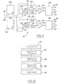
- the device comprises a time base 100, controlled by a processing unit 200.
- the time base 100 attacks on the one hand a measurement unit 300 receiving the capacitor Cx to test, on the other hand a unit 400 connected to the measurement unit 300, which is sensitive to the response of the capacitor to the periodic slot and which performs the sampling and an analog / digital conversion of the signal, the latter then being applied to the aforementioned processing unit 200, which then determines said parameters Coo, Rs, Ci and Ri.
- the processing unit 200 ensures, in addition to controlling the sequencing of the different bursts of slots generated by the time base 100 and the processing tasks proper, relations with conventional peripherals, such as printer 500, display screen or keyboard 600 and additional memory 700, and if necessary with an operating robot 800.
- the robot 800 can be used to ensure automatic insertion of the capacitors Cx into the measurement chain integrated into the unit 300, and an evacuation of said capacitors, with classification, based on an exploitation of the output information.
- the essential function of the time base 100 is to generate the excitation slots and the sampling pulses.
- the purpose of the time base 100 is to generate several ranges of periods of excitation slots accompanied by sampling pulses progressively offset from the successive times of application of the stimulus, as well as the introduction of fixed delays, to allow safe observation of the start of the response.
- the sampling times must constantly respect the minimum analog / digital conversion time.
- the processing unit applies sequencing signals on the time base 100.
- the processing unit 200 ensures the general reset of the device. To simplify the representation, the reset inputs of the components of the time base 100 have not been shown in FIG. 8.
- the processing unit 200 generates at its output 201 a signal for validation of the first range of excitation and sampling slots.
- a first series of data is acquired by sampling and conversion of the signal present at the output of the measurement unit 300.
- the processing unit 200 counts the number of acquired data.
- the output 201 is disabled and the processing unit generates on its output 202 a signal for validation of the second range of excitation slots and sampling pulses. A second series of data is then acquired.
- the output 202 is disabled and the processing unit generates on its output 203 a slot of 800 ms and a period sampling signal for example equal to 160 they.
- the different periods of the excitation slots and of the sampling pulses of the first and second bursts are determined by divisions of the frequency of a clock 101.
- the latter could be composed for example of an oscillator with logic gates controlled by a quartz of frequency 5 MHz.
- the first burst of excitation slots is obtained by dividing the clock frequency by 1000 which leads to slots of period 200 ⁇ s, while the sampling pulses are obtained by dividing the clock frequency by 1001 which leads to pulses with a period of 200.2 ⁇ s.
- the frequency of the clock 101 is divided by 500 thanks to three counters 102, 103, 104, connected in cascade, which ensure respectively a division by 10, 10 and 5 and which attack (counter 104) a monostable M105 which controls the counters 102, 103 and 104 by its output Q. More specifically, the monostable M105 controls by its output U the counting, in the absence of a reset signal on the counters 102, 103 and 104.
- the output Q of the monostable M105 controls by the rising edge a monostable M106 which has a pulse duration ⁇ , as shown on the second and third lines of the timing diagram of FIG. 9 the first line of which schematically represents the signal at the output of the clock 101.
- the Q output of the monostable M106 attacks a JK107 flip-flop which changes state with each falling edge of the signal at the Q output of the monostable M106, as shown in the fourth line of FIG. 9.
- the output of this JK107 flip-flop is connected to the first terminal 109 of an AND gate 108 which receives on its second terminal 110 the validation signal of the first burst (output 201 of the processing unit 200).
- the output of the AND gate 108 is connected to the first terminal 112 of an OR gate 111. It will be noted that the flip-flop JK107 ensures a division by two of the frequency of the signal at the output of the monostable M106.
- the output 113 of the OR gate 111, on which the excitation slots are available, is connected to the measurement unit 300.
- the delay introduced by the monostable M106 with respect to the origin of the times, is intended to compensate for the delay brought by the sampler-blocker integrated into the unit 400. This provision will be explained later.
- said delay p introduced by the monostable M106 is chosen to be greater than the minimum duration of the sampling pulse, so that one obtains some samples of zero value taken during the low level of the slot. stimulation corresponding to the reset phase.
- the signals present at the output of the flip-flop JK107 are found at the output 113 of the OR gate 111 when the AND gate 108 is validated, that is to say when a high level signal is applied to the input 110 of this by the output 201 of the processing unit.
- the sampling pulses are obtained by dividing the frequency of the clock 101 by 1001 to obtain pulses of period 200.2 they.
- This division by 1001 is operated by the element referenced 120 in FIG. 8.
- this element 120 may consist of four counters 121, 122, 123 and 124 capable of counting from N to 9 with 0 ⁇ N ⁇ 9 and prepositioned to 8999.
- the counting chain 121-122-123 and 124 attacks a monostable M125 which by its output Q controls the counting in the absence of a reset signal on the counters 121, 122, 123 and 124.
- the Q output of the monostable M125 will be validated when the count reaches 10,000, which from 8,999 to 10,000 leads to a division by 1001.
- the output Q, referenced 126 of the monostable 125, which constitutes the output of the element 120, is connected to the first terminal 129 of an AND gate 127, which receives on its second terminal 128 the validation signal of the first burst issued of the output 201 of the processing unit 200.
- the output 130 of the AND gate 127 is connected to the first terminal 132 of an OR gate 131 with three inputs, the output 135 of which is connected to the sampling and analog / digital conversion unit 400.
- the signals present at the output 126 of the monostable 125 are found at the output 135 of the OR gate 131 when the AND gate 127 is enabled, that is to say when a high level signal is applied to the input 128 of it by the output 201 of the processing unit.
- the second burst of excitation slots is obtained by dividing by 10 the frequency of the excitation slots of the first range, which leads to stimulation slots of periods of 2 ms, while the sampling pulses of the second burst are obtained by dividing the clock frequency by 1010, which leads to pulses of 202 ps periods.
- the output of the flip-flop JK107 is connected to the first terminal 141 of an AND gate 140 with two inputs, which receives on its second terminal 142 the validation signal of the second burst (output 202 of the processing unit 200).
- the output 143 of the AND gate 140 is connected to the input of a member 144 ensuring a division by 10 of the frequency of the signal present at the output of the flip-flop JK107.
- the output 145 of the member 144 is connected to the first terminal 147 of a gate 146 of the ET type, with two inputs, which receives on its second input terminal 148 the validation signal of the second burst (output 202 of the processing unit 200).
- the output 149 of the AND gate 146 is connected to the second input terminal 150 of the aforesaid OR gate 111.
- the signals present at the output of the divider member 144 are found at the output 113 of the OR gate 111 when the AND gate 146 is validated, that is to say when a high level signal is applied to the input 148 thereof by the output 202 of the processing unit 200.
- the sampling pulses accompanying this second burst are obtained by dividing the frequency of the clock 101 by 1010 to obtain pulses of period 202 ⁇ s.
- This division by 1010 is operated by the element referenced 160 in FIG. 8.
- this element 160 could consist, similar to the aforementioned element 120 of four counters 161, 162, 163 and 164 capable of counting from N to 9, with 0 ⁇ N ⁇ 9 and prepositioned at 8990.
- the counting chain 161-162-163 and 164 attacks a monostable M165 which, by its output Q controls the counting of the aforementioned counters 161, 162, 163 and 164 in the absence of reset signal thereon .
- the input of the first counter 161 of the element 160 is connected to the output 171 of an AND gate 170 with two inputs.
- the inputs 172 and 173 of this gate 170 are respectively connected to the output of the clock 101 and to the output 202 of the processing unit 200 validating the second range.
- the Q output of monostable 165 will be validated when the count of element 160 has reached 10,000, which from 8,990 to 10,000 leads to division by 1010.
- the output 175 of the AND gate 172 is connected to the second terminal 133 of the above-mentioned OR gate 131 with three inputs, the output 135 of which is connected to the unit sampling and analog / digital conversion 400.
- pulses with a period of 202 microseconds are obtained, slightly greater than a submultiple of the period of the stimulation slots and which therefore gradually shift relative to them. this.
- the signals present at the output 166 of the monostable M165 are found at the output 135 of the OR gate 131, when the AND gate 172 is validated, that is to say when a high level signal is applied to the input 173 of the latter by the output 202 of the processing unit 200.
- the third range is made up of a single slot whose duration is for example 800 ms, with real-time sampling of tight steps up to 32 ms and more loose steps for the rest of the time.
- the stimulation step of 800 ms duration is generated by the processing unit 200 on its output 203.
- the latter is connected to the third input terminal 151 of the OR gate 111.
- the real-time sampling is controlled directly by the processing unit 200, by its output 204 which is connected to the third terminal 134 of the OR gate 131.
- successive responses to the periodic stimulation slots can be considered as the superimposition of the beginnings of the response at the level and of stages whose value in the first slot evolves from one slot to another.
- the Applicant proposes to correct the amplitude value measured during the nth slot with the value of the amplitude measured at equivalent time during the first slot.
- the Applicant proposes to take a reference sample, for each stimulation slot, at a predetermined fixed instant thereof.
- the Q output of this M106 monostable has a falling edge synchronous with the original clock pulses.
- Said output Q of the monostable M106 is connected to the input 177 of a flip-flop JK176 which performs a division by 2 of the frequency of the signals coming from the monostable 106. Consequently the output of the flip-flop JK176 delivers slots of periods 200 ⁇ s not lagging behind the origin of time.
- the output 178 of the flip-flop JK176 is connected to the first input terminal 180 of an AND gate 179 with two inputs, which receives on its second input 181 the validation signal of the first range from the output 201 of the processing unit 200.
- the output 182 of the AND gate 179 is connected to the first input terminal 137 of an OR gate 136 with two inputs, the output 139 of which is connected to the sampling unit 400, in order to order the acquisition of reference samples, during the first range.
- the output 178 of the flip-flop JK176 is connected to a first input terminal 184 of an AND gate 183 with two inputs.
- the second terminal 185 of this AND gate 183 is connected to the output 202 of the processing unit 200 validating the second range.
- the output 186 of the AND gate 183 is connected to the input of a frequency-dividing member 187 by 10, the output of which 188 is connected to the first input terminal 190 of an AND gate 189 with two inputs, which receives on its second input terminal 191 the second range validation signal from output 202.
- the output 192 of the AND gate 189 with two inputs is connected to the second input terminal 138 of the OR gate 136.
- the dividing member 187 generates at the output slots of periods 2 ms.
- the signals present at the output of the flip-flop JK176 are found at the output 139 of the OR gate 136 when the AND gate 179 is validated, that is to say when a high level signal is applied to the input 181 of it by the output 201 of the processing unit.
- a signal with a period of 2 ms is present at the output of the dividing member 187 when the AND gate 183 is enabled, (when a high level signal is applied to the input 185 thereof by the output 202 of the processing unit, and therefore the AND gate 189 being validated in parallel), the signal present at the output of the member 187 is found at the output 139 of the OR gate 136.
- the counters 102, 103, 104, 121, 122, 123, 124, 161, 162, 163, and 164 are of the type 74 192
- the monostables M105, M106 and M125, M165 are of type 74 122
- flip-flops JK107, 176 are of type 7476.
- the measurement unit 300 illustrated diagrammatically in FIG. 7 and detailed in FIG. 10 has the function of operating a shaping of the excitation slots coming from the output 113 of the time base 100, from the amplitude point of view. , rise time and reference to zero of the low level, to detect the response of the sample to stimuli, through the measurement chain formed by the capacitive divider Cx and Cr, while achieving the isolation of the exit point of the chain measurement and the transfer of the response without disturbance, as well as by carrying out the reset to zero of the point of exit of the measurement chain during the idle times of the stimulus.
- the shaping of the stimulation slots is carried out by a shaping stage comprising an amplifier stage 302 and a transistor T ,. More specifically, the output 113 of the time base 100 is connected to the input 301 of the measurement unit 300, which is itself connected to the input 303 of the abovementioned amplifier operator 302.
- the output 304 of this operator is connected via a resistor R305 to the base of the transistor T, of the NPN type mounted as a common collector.
- the collector of transistor T is in fact connected to a positive supply terminal + VCC.
- the collector of transistor T is also connected to the output 304 of the operator 302 via a resistor R306.
- the emitter of transistor T is connected to the ground of the assembly via a resistor R307.
- the emitter of transistor T is also connected to a first terminal of capacitor Cx to be tested.
- the second terminal of this capacitor is connected to a first terminal of the capacitor Cr integrated in the measurement chain, which is connected by its second terminal to the ground of the assembly.
- the measurement chain is attacked by stimulation slots from the transistor emitter T ,.
- the reference capacitor Cr is chosen to be of the order of magnitude approximately 1000 times greater than the nominal value of the capacitor Cx to be tested.
- the measurement unit 300 advantageously includes means making it possible to modify the reference capacitor Cr by switching. These means have not been shown in FIG. 10 in order to simplify the illustration.
- the output of the measurement chain is taken between the common point between the capacitor Cx to be tested and the reference capacitor Cr.
- the voltage level at the output of this cell is low (around 15 mV).
- the measuring chain is shielded, as shown in 308, in FIG. 10, in order to avoid the superposition of noise on the useful signal.
- This device operates in parallel on the reference capacitor Cr. Of course, this device must at least disturb the behavior in pure capacitance of the reference capacitor. Nevertheless, the Applicant has demonstrated that over the whole range of useful frequencies, the reset device, during the active phase of the process, that is to say the high level of the stimulation window, can be likened to a scheme. equivalent combining in parallel a constant capacity and a constant resistance.
- Said capacity of the order of a few pF, is added to the capacity of the reference capacitor Cr and can easily be taken into account.
- the parasitic resistance due to the reset device is very high and does not, in practice, disturb the capacitive behavior of the reference capacitor.
- the input 301 of the measurement unit 300 is connected to the input 309 of an amplifier stage 310.
- the output 311 of this is connected via a resistor R312 to a negative supply terminal -V cc .
- the output 311 of the amplifier stage 310 is connected to the cathode of a Zener Z diode 313 .
- the anode of this diode Z 313 is connected via a resistor R314 to the ground of the assembly.
- the anode of this diode Z 313 is connected to the base of a bipolar PNP T2 transistor mounted as a common emitter.
- the emitter of this transistor T2 is in fact connected to the ground of the assembly, while its collector is connected to a negative supply terminal - V DC via a load resistor R315.
- collector of transistor T2 is connected to the gate of a field effect transistor T3, the source-drain channel of which is inserted, by means of a resistor R316 between the ground of the assembly and the point common to capacitors to be tested Cx and reference Cr.
- the transistor T2 is conductive and the field effect transistor T3 whose gate is brought to zero potential is conductive.
- the transistor T2 is blocked and brings the gate of the field effect transistor T3 to a strongly negative potential blocking the latter.
- the output of the Cx-Cr measuring chain is connected to a decoupling stage which aims to transmit the response while modifying the admittance of the reference capacity Cr as little as possible.
- This decoupling stage is formed by an operational amplifier OP317 with internal frequency correction.
- This operational amplifier OP317 is connected directly by one of its inputs to the point common to the capacitors to be tested Cx and of reference Cr, while its output is connected directly to its second input, to form a feedback loop.
- the OP317 amplifier is thus mounted as a voltage follower.
- such an operational amplifier OP317 can be of the LH 0052 type.
- the Applicant has found that such a device gave full satisfaction.
- the above circuit has an input resistance greater than 10 10 ohms.
- the input impedance due to the operational amplifier OP317 introduces an error on the tangent the angle of dielectric losses, as the order of 10 -4 at 10 Hz. in addition, this error decreases rapidly with increasing frequency.
- the above-mentioned decoupling stage is followed by at least one amplification stage.
- the decoupling stage OP317 is followed by two inverting amplifiers connected in cascade.
- the output of the amplifier OP317 is connected to the mass of the assembly by means of a resistor R318. Furthermore, the output of the amplifier OP317 is connected via a resistor R319 to the first input terminal of an amplifier OP320, the second input of which is connected to ground. The output of this operational amplifier OP320 is looped back to said first input thereof via a resistor R321. The output of the OP320 amplifier is connected via a resistor R322 to the first input of a second OP323 amplifier mounted as an inverter. To do this, the second input 324 of the amplifier OP323 is connected to ground while the output 325 of this same amplifier is looped back to the first input via a resistor R326.
- the output 325 of the operational amplifier OP323 is connected to the sampling unit 400.
- the operational amplifiers OP320 and OP323 are of the AD507 and AD509 type, while the amplifier stages 302 and 310 are of the 7416 type.
- the test device according to the present invention must allow the control of the usual capacitor values, and must therefore cover at least the range from 1 pF to ⁇ F. This range cannot be covered with a single reference capacitor. To do this, the Applicant proposes to divide the measurement process into two main ranges.
- the first main range concerns the testing of capacitors with a capacity between 0.3 pF and 30,000 pF.
- the second main range concerns the testing of capacitors with a capacity greater than 30,000 pF.
- the first main range is itself divided into five auxiliary sub-ranges.
- the first auxiliary sub-range concerns the capacitors to be tested with a capacity ranging from 0.3 to 3 pF.
- This first auxiliary sub-range uses a reference capacity of 1000 pF.
- the second auxiliary sub-range concerns the capacitors to be tested with a capacity ranging from 3 to 30 pF.
- This second auxiliary sub-range uses a reference capacity of 10,000 pF.
- the third auxiliary sub-range concerns the capacitors to be tested with a capacity ranging from 30 to 300 pF.
- This third auxiliary sub-range uses a reference capacity of 100,000 pF.
- the fourth auxiliary sub-range concerns the capacitors to be tested with a capacity ranging from 300 to 3000 pF.
- This fourth auxiliary sub-range uses a reference capacity of 1 pF.
- the fifth auxiliary sub-range concerns the capacitors to be tested with a capacity ranging from 3000 pF to 30,000 pF.
- This fifth auxiliary sub-range uses a reference capacity of 10 ⁇ F.
- the Applicant proposes, to avoid a loss of definition, to invert the reference capacitor Cr and the capacitor to be tested Cx, with respect to the mode shown in FIG. 10.
- the reference capacitor Cr on which the stimulation slots are applied must respect the Cr-Cx / 1000 relationship.
- the response detected by the decoupling stage (amplifier OP317) is then taken across the terminals of the capacitor to be tested Cx.
- the Applicant has demonstrated that the response thus taken responds to the relationship: It will indeed be noted that this expression (13), applicable for the second main measurement range, is very close to the relationships previously exposed. Therefore, the processing unit can use the same type of processing and the same algorithms as those which will be discussed later.
- the sampling and conversion unit 400 schematically represented in FIG. 7 and shown in more detail in FIG. 11 has the essential function of operating the sampling of the data, while ensuring the transfer interface between the unit 300 and the processing unit 200.
- sampling and conversion unit 400 is to transform sample values into a binary code (on 10 bits). born from the analog response from the measurement unit 300.
- the sampling and conversion unit 400 is connected to the measurement unit 300 via its input 402, to the time base 100 via its inputs 401 and 421, and finally, downstream, to the processing unit 200 via its outputs 451, 452 and 461, 462.
- the sampling unit 400 comprises in cascade, a blocking sampler 405, an adjustable gain amplifier 415 and an analog / digital converter 450.
- the device is suitable for taking, in addition to the measurement samples which pass through the blocking sampler chain 405 - amplifier 415 and converter 450, reference samples taken at a fixed instant from each stimulation slot.
- the sampling and conversion unit comprises, in parallel with the above-mentioned chain, a second chain through which the reference data pass and which also includes in cascade a blocking sampler 425 followed by an adjustable gain amplifier 435 and an analog / digital converter 460.
- the purpose of the blocking sampler 405 is to ensure, under the control of the time base 100 the acquisition and then the maintenance of the analog samples.
- the blocking sampler 405 shown diagrammatically in FIG. 11, essentially comprises an operational amplifier 406, a controllable switch 409 and an amplifier stage 411.
- a first input 407 of the operational amplifier 406 is connected to the input 402 of the sampling unit 400, to receive the analog signals coming from the measurement unit 300.
- the output 408 of the operational amplifier 406 is capable of being connected via the controllable switch 409 to the input 412 of the amplifier stage 411.
- the output of this amplifier stage 411 is connected to the second input 414 of the operational amplifier 406.
- the controllable switch 409 is controlled by the state of a signal applied to the input 410 of the blocking sampler 405.
- This input 410 is also connected to the output U of a monostable 420 whose input is connected to the input 401 of the unit 400.
- This input 401 is connected to the output 135 of the time base 100 for receiving the sampling pulses generated by it.
- the second blocking sampler 425 comprises an operational amplifier 426, a first input 427 of which is connected to the input 402 of the sampling unit to receive the analog signals coming from the measurement unit 300.
- the output 428 of the operational amplifier 426 can be connected via a controllable switch 429 to the input 432 of an amplifier stage 431 whose output is looped back to the second input 434 of the amplifier 426.
- L the controllable switch 429 is controlled by the state of the input 430 of the circuit 425.
- This input 430 is connected to the output Q of a monostable 440 whose input is connected to the input 421 of the unit 400.
- This input 421 is connected to the output 139 of the time base to receive the reference sampling pulses.
- the blocker samplers 405, 425 can be formed from the AD 582 type circuit sold by the company ANALOG DEVICES. Such a circuit can ensure the sampling of analog signals of 10 V peak to peak in a time of 6 seconds. Furthermore, the blocker samplers 405, 425 have a holding time for information on their respective output 413, 433 of the order of 25 they, entirely compatible with the conversion time of 25 they required by the converters 450, 460 , arranged downstream.
- sampling of the measurement data is carried out by the closing-opening process of the controllable switch 409 integrated into the blocking sampler 405, this closing-opening process being controlled by the sampling pulses from output 135 of time base 100.
- the reference sampling is established by the closing-opening process of the controllable switch 429 integrated into the sampler 425, this closing-opening process being controlled by the sampling pulses coming from the output 139 of the time base 100.
- each of the blocking samplers 405, 425 has a non-zero sampling gate closing time, as well as a time for tracking the output voltage relative to the non-zero input voltage.
- the stimulation slots present on the output 113 of the time base 100 are delayed with respect to the sampling pulses.
- the first samples likely to be retained are established on the low level of the stimulation slots and are therefore of zero value. Therefore, by retaining the first non-zero sample as the first valid sample, the delays specific to the sampling-blocking process do not disturb the measurement.
- the value at the origin of the response curve is determined not on the basis of the first acquired data, but by extrapolation on the basis of the second and the third. data.
- the outputs 413 and 433 of the sampler-blockers 405, 425 are respectively connected to the inputs of amplifiers with adjustable gain 415, 435.
- the latter make it possible to adapt the dynami that of output of the sampler-blocker 405, 425 respectively to the dynamic input of the analog / digital converter 450, 460.
- the respective outputs 416 and 436 of the amplifiers 415 and 435 are connected to the inputs of the converters 450 and 460.
- the latter can be formed, for example, of the AD 571 type circuit. Such circuits convert an sampled analog input signal into words 10 bits.
- the digital signals generated respectively by the converters 450 and 460 are available on the respective data buses 452 and 462 of these devices, which are connected to the processing unit 200.
- the converters 450 and 460 when the digital data are available on the aforementioned buses 452 and 462, the converters 450 and 460 generate on their outputs 451, 461, coded DR, a low level signal.
- the digital data remains present on the buses 452, 462, for processing by the processing unit 200, until the end of the control window applied on the converters 450 and 460 by the Q output of the monostables 420 and 440 respectively, as shown in Figure 11.
- the essential functions of this unit are to control the time base 100 by means of sequencing signals, for the generation of the different bursts of excitation slots and of sampling pulses and to ensure relations with conventional peripherals. 500, 600 and 700 and, where appropriate, a robot 800, as well as processing signals from the sampling unit 400 and analog / digital conversion.
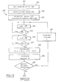
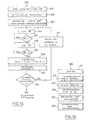
- the processing process successively comprises an initialization phase 210, a phase 220 of acquisition of the first range of data, a phase 240 of acquisition of the second range of data, a phase 260 of acquisition of the third range of data and finally a phase 270 of actual processing.
- the initialization phase 210 makes it possible to introduce the coefficients necessary for the completion of the processing phase 270, that is to say the coefficients necessary for the determination of the parameters (steps 272, 273, 274 and 275) and tolerance standards for classifying capacitors (step 276).
- the acquisition of data which aims to store these before the processing operation, is divided into three phases 220, 240 and 260 respectively, corresponding to the three ranges of excitation slots. and sampling pulses defined by the time base 100.
- the subroutines of the first and second acquisition phases 220, 240 take into account in addition to the measurement sample due to the sampling pulses generated at the output 135 of the time base 100, l ' reference sample due to the sampling pulses generated at the output 139 of the time base 100, to compensate for the effect of the stages induced by the reset, and which evolves from one slot to another.
- the process 220 begins with a step 221 of resetting to zero with time delay of the time base 100.
- Step 221 is followed by a step 222 of initializing the registers determining on the one hand the number of data previously stored and on the other hand the number of the address of the first data.
- Step 222 is followed by step 223 during which the processing unit validates the output 201, by applying a high level signal thereto, and invalidates the outputs 202, 203 and 204 by applying a signal. low level on these.
- the system is then ready for data acquisition.
- This acquisition is however conditioned by the DR line test of the analog / digital converter 450. Indeed, a high level signal on the DR line indicates that data is being converted, and transfer should only be authorized when the DR line goes low.
- This waiting process is determined by schematic steps 224 to 227.
- step 224 which follows step 223, the processing unit reads the state of the line DR and tests the state of the line DR in step 225.
- step 225 is followed by step 226 which will determine a waiting loop.
- step 224 is repeated after step 225.
- step 226 the processing unit 200 again reads the state of the line DR and this state is tested in the next step 227.
- step 226 of reading the state of the line DR is repeated.
- step 227 is followed by step 228 of correction.
- the aim of this correction procedure is to cancel the effect of the stages due to the resetting of the signal during low half-vibrations of the excitation slots.
- the correction on the measurement signal Y nm taken at the instant m of the n th excitation slot is carried out using the reference signals (due to the reference sampling signals generated on the output 139 of the time base 100 ).
- the correction uses, on the one hand, the reference sample Y ,, taken during the first excitation niche at time r and the reference sample Y nf taken in the n th niche at the equivalent time r.
- the correction stage 228 is followed by the storage step 229.
- This last step 229 is followed by a test step 230 during which the processing unit 200 searches if the number of stored data equals a predetermined number p.
- p 500 since 500 data of 0.2 ⁇ s must be taken.
- step 224 is repeated after incrementing the data storage address during intermediate step 231.
- step 230 If the test in step 230 is positive, the acquisition phase of the first range is completed and this step 230 is followed by the phase 240 of acquisition of the second range.
- the process 240 begins with a step 241 of resetting with time delay of the time base 100.
- Step 241 is followed by a step 242 of initializing the registers determining on the one hand the number of data memorized during the second acquisition phase, and on the other hand the number of the memory storage address. the first data of the second acquisition phase.
- Step 242 is followed by step 243 during which the processing unit 200 validates the output 202, by applying a high level signal thereto, and invalidates the outputs 201, 203 and 204, by applying a low level signal on them.
- the system is then ready for the second phase of data acquisition.
- step 244 which follows step 243, the processing unit 200 reads the state of the line DR, and tests the state of this line in step 245.
- step 245 If the line DR is at a high level, a piece of data being converted, step 245 is followed by step 246 which will determine a waiting loop.
- step 244 is repeated after step 245.
- step 246 the processing unit 200 again reads the state of the line DR and this state is tested in the next step 247.
- step 246 of reading the state of the line DR is repeated.
- step 247 is followed by step 248 of correction.
- This correction process is carried out on the measurement signal Y nm taken at the instant m from the n th excitation slot using the sample. of reference Y lr taken during the first excitation niche at time r and the reference sample Y nr taken in n th niche at the equivalent time r, on the basis of the relation.
- the correction step 248 is followed by the storage step 249.
- This storage step 249 is followed by a test step 250 during which the processing unit 200 searches if the number of stored data equals a predetermined number q.
- step 244 is repeated after defining a new storage address in intermediate step 251. This will be explained below.
- step 250 If on the other hand, the test in step 250 is positive, the second acquisition phase 240 is completed, and step 250 is followed by step 260 of acquisition of the third range.
- the data are not obtained in their natural order: 1st, 2nd ... but according to a sequence presenting an interlacing: 1st, 6th, 11th ... 2nd, 7th, 12th. due to the fact that 5 samples are taken for each stimulation slot.
- step 251 the processing unit must define the addresses for storing the data according to an interlaced sequence respecting the actual order of acquisition of the data.
- the processing unit 200 must take into account the reference samples as and when they are generated.
- the third acquisition phase 260 aims to study the behavior of the capacitor at low frequency.
- the processing unit 200 directly generates a single stimulation step as well as sampling pulses in real time.
- the third acquisition phase 260 can be operated on the basis of the following three sub-steps.
- the acquisition of 200 data is operated continuously with a sampling step of 160 ⁇ s up to 32 ms.
- the acquisition of 9 data is operated with a step of 8 ms up to 96 ms.
- this third acquisition phase has 223 points.
- the processing phase 270 begins with a step 271 of smoothing the raw data stored not in the order of acquisition but in the natural order of the samples.
- the aim of this smoothing step is to refine the data, affected by random disturbances mainly due to the quantization error and the error over the acquisition time.
- the smoothing is carried out by a mobile averaging method.
- the average value Ym of a sample assigned to time is defined. based on the relationship: However, the number of support points considered for establishing the moving average increases from the start of each range to the end of it to take into account the fact that the variations of the signal are faster at the start of the range than at the end of the range.
- the first 10 points are not smoothed, the following points are smoothed on three points and the end of the range uses a press on 8 points.
- the processing unit then proceeds to determine the parameters during steps 272, 273 and 274 which will be explained later.
- the Applicant has determined on this basis that the law of correspondence being linear, it is possible to acquire the characteristic parameters directly on the function y (t) in the form of intermediate parameters, during steps 272, 723 and 274, by subsequently transforming these into real parameters Coo, 1 / Rs, Ci, Ri and Cs in the consecutive step 275.
- step 272 the processing unit 200 determines the intermediate parameters ys and 1 / ps.
- the parameter 1 / ps is determined by the slope of the curve for long times.
- the parameter ys is determined by extending the slope at the origin.
- the slope of the curve is determined at several points, for example at times 32 ms, 96 ms and 720 ms and the relative values of the slope are compared.
- the capacitor has a conductance behavior of 1 / ps.
- the processing unit 200 determines that the capacitor exhibits a conductance behavior determined by the slope at instant 96 ms, from frequency 1 / 2 ⁇ 96 ms ⁇ 1.6 Hz.
- the parameter ys is then determined on the basis of a relation equivalent to relation (23).
- the three slopes are different, they indicate the presence of a relaxation phenomenon which evolves over time.
- step 273 the processing unit 200 determines the intermediate parameter ⁇ ⁇ .
- the parameter y corresponds to the first stored value.
- this point is marred by an error due to the uncertainty on the sampling time at the start of the response, on the one hand, and on the value of the first stored point, on the other hand.
- the parameter ⁇ ⁇ is determined by extrapolation from the second and third stored points.
- t 2 represents the sampling instant for the 2nd stored point
- 8T represents the sampling step.
- the time t'o of the true origin of the response is unknown. It can be equal to t 2 - ⁇ T in the case where an ideal sampling of the first point is made and equal to t 2 -2 ⁇ T in the other extreme case, which leads to locating on average the origin at time:
- the Applicant has determined that the error made in the determination of the parameter ⁇ ⁇ , by virtue of the aforementioned process, error which is due on the one hand to the uncertainty on the true origin time included in the interval t 2 - 2 ⁇ T ⁇ t'o ⁇ t 2 - 8T and on the other hand a certainty on the amplitude, is negligible.
- step 274 the processing unit 200 determines the intermediate parameters 1 / pi and yi.
- the intermediate parameter 1 / pi is, in theory, obtained by subtracting from the initial slope the term of conductivity 1 / ps, since the initial slope equals 1 / ⁇ s + 1 / ⁇ i.
- the relaxation time ⁇ j of each active branch of the FOSTER model is determined by detection of the abscissa of the maximums of the curve ⁇ '(logt).
- the processing unit 200 then detects the ordinates u (tj) and ⁇ (tj + 1) of the curve ⁇ (t) for the times tj and tj + 1. The difference between these ordinates ( ⁇ (tj + 1) - ⁇ (tj) gives directly the value 1 / T i and therefore the value ⁇ i.
- the processing unit 200 determines the real parameters, from the aforementioned intermediate parameters, on the basis of relations (17) to (22).
- the signal at the output of the measurement unit 300 responds to the relationship: relationship in which
- V represents the amplitude of the excitation slot
- G represents the gain of the system
- H represents a constant linked essentially to the reset device connected to the terminals of the reference capacitor.
- step 276 the processing unit 200 operates a classification of the capacitors.
- This classification is to detect the compliance or non-compliance of the capacitors with the standards provided for in a specification and consequently to monitor the quality of the manufacturing. To operate the classification or compare the real parameters Coo mes , Csmes and Rmes with ideal parameters Cooth, Csth and Rth stored in memory during the initialization step 210.
- a compliance signal is sent.
- step 210 a step of validity or tolerance in percentage ( ⁇ x%) of the nominal value Cn is memorized in step 210.
- the processing unit 200 emits a signal indicating the conformity of the capacitor with regard to the parameter Coo.
- the processing unit 200 proceeds in the same way for the parameters Cs and Ri.
- the results of the three classification procedures relating to the three parameters are stored in memory.
- the memorized signals can be used to control the robot 800 playing the role of sorting machine.
- Sorting may require, for example, that the three parameters comply with standards, or take into account the values of each of these three parameters separately.
- step 274 it is possible to avoid determining the slope ⁇ (t) for the evaluation of the parameters 1 / pi and Ci.
- the processing unit 200 may be formed for example of a microcomputer card of the ECB85 type sold by the company SIEMENS. It will be recalled that this card includes a microprocessor 8085, two parallel input / output doors 8185, an active static RAM memory with a capacity of 1 byte, a monitor program and a circuit type 8279 providing the interface with the keyboard 600.
Landscapes
- Physics & Mathematics (AREA)
- General Physics & Mathematics (AREA)
- Engineering & Computer Science (AREA)
- Power Engineering (AREA)
- Measurement Of Resistance Or Impedance (AREA)
- Investigating Or Analyzing Materials By The Use Of Electric Means (AREA)
- Inorganic Insulating Materials (AREA)
- Electrotherapy Devices (AREA)
- Testing Electric Properties And Detecting Electric Faults (AREA)
- Fixed Capacitors And Capacitor Manufacturing Machines (AREA)
Claims (38)


Priority Applications (1)
| Application Number | Priority Date | Filing Date | Title |
|---|---|---|---|
| AT85400873T ATE41709T1 (de) | 1984-05-10 | 1985-05-06 | Verfahren und schaltung zur pruefung dielektrischer materialien, insbesondere kondensatoren. |
Applications Claiming Priority (2)
| Application Number | Priority Date | Filing Date | Title |
|---|---|---|---|
| FR8407196A FR2564205B1 (fr) | 1984-05-10 | 1984-05-10 | Procede et dispositif pour le test rapide de condensateurs et de materiaux dielectriques |
| FR8407196 | 1984-05-10 |
Publications (2)
| Publication Number | Publication Date |
|---|---|
| EP0165109A1 EP0165109A1 (de) | 1985-12-18 |
| EP0165109B1 true EP0165109B1 (de) | 1989-03-22 |
Family
ID=9303829
Family Applications (1)
| Application Number | Title | Priority Date | Filing Date |
|---|---|---|---|
| EP85400873A Expired EP0165109B1 (de) | 1984-05-10 | 1985-05-06 | Verfahren und Schaltung zur Prüfung dielektrischer Materialien, insbesondere Kondensatoren |
Country Status (6)
| Country | Link |
|---|---|
| US (1) | US4683417A (de) |
| EP (1) | EP0165109B1 (de) |
| JP (1) | JPS6150072A (de) |
| AT (1) | ATE41709T1 (de) |
| DE (1) | DE3569041D1 (de) |
| FR (1) | FR2564205B1 (de) |
Families Citing this family (13)
| Publication number | Priority date | Publication date | Assignee | Title |
|---|---|---|---|---|
| FR2584196B1 (fr) * | 1985-07-01 | 1988-04-22 | Univ Rennes | Procede et dispositif pour le test rapide, par reflectrometrie, dans les gammes v.h.f., de composants passifs |
| FR2661509B1 (fr) * | 1990-04-27 | 1992-06-19 | Europ Composants Electron | Procede de controle des mesures realisees dans un appareil de test et de tri d'articles miniatures. |
| US5469364A (en) * | 1993-03-15 | 1995-11-21 | Hughey; Bradley W. | Apparatus and methods for measuring and detecting variations in the value of a capacitor |
| US6054864A (en) * | 1996-11-18 | 2000-04-25 | Butts; Joseph R. | In-circuit capacitor checker |
| TW460701B (en) * | 2000-01-20 | 2001-10-21 | Winbond Electronics Corp | Improved test circuit of TDDB |
| FR2818554B1 (fr) * | 2000-12-22 | 2003-03-28 | Ela Medical Sa | Procede de mesure de l'impedance complexe d'une sonde de dispositif medical implantable actif, notamment de stimulateur cardiaque, defibrillateur et/ou cardioverteur |
| EP1865519A4 (de) * | 2005-03-24 | 2018-03-14 | Showa Denko K.K. | Vorrichtung und verfahren zur herstellung eines festelektrolytkondensators |
| WO2007075887A2 (en) * | 2005-12-21 | 2007-07-05 | Weiss Instruments, Inc. | Micropower voltage-independent capacitance measuring method and circuit |
| WO2008025308A1 (de) * | 2006-08-30 | 2008-03-06 | Siemens Aktiengesellschaft | Verfahren zum erzeugen eines fehlersignals, das einen fehler in einer kondensatorandordnung angibt und elektrisches schutzgerät zur durchführung des verfahrens |
| DE102008044908A1 (de) * | 2008-08-29 | 2010-03-04 | Lemförder Electronic GmbH | Anordnung zur Messung wenigstens eines Wertes einer an einer elektronischen Komponente anliegenden Spannung |
| JP2010230688A (ja) * | 2010-07-06 | 2010-10-14 | Nippon Chemicon Corp | 電解コンデンサの測定方法及び測定プログラム |
| US10006956B2 (en) * | 2015-03-26 | 2018-06-26 | Lenovo Enterprise Solutions (Singapore) Pte. Ltd. | Systems and methods for determining an operational condition of a capacitor package |
| CN109828157B (zh) * | 2019-01-30 | 2020-12-25 | 东南大学 | 一种介质基片介电常数测量机构及其测量方法 |
Family Cites Families (8)
| Publication number | Priority date | Publication date | Assignee | Title |
|---|---|---|---|---|
| BE792405A (fr) * | 1971-12-08 | 1973-03-30 | Paratronic Ag | Dispositif pour mesurer sans les detruire l'epaisseur de revetements electriquement non conducteurs sur des supports electriquement conducteurs |
| JPS539542B2 (de) * | 1972-09-21 | 1978-04-06 | ||
| US4282480A (en) * | 1978-05-02 | 1981-08-04 | Matsushita Electric Industrial Co., Ltd. | Apparatus for humidity detection |
| US4216424A (en) * | 1978-10-30 | 1980-08-05 | Vette Carl W | Method and apparatus for testing electrolytic capacitors |
| US4404481A (en) * | 1980-10-20 | 1983-09-13 | Matsushita Electric Industrial Co., Ltd. | Capacitance to voltage conversion apparatus |
| US4330777A (en) * | 1980-11-05 | 1982-05-18 | The United States Of America As Represented By The United States Department Of Energy | Device for detecting imminent failure of high-dielectric stress capacitors |
| AT377859B (de) * | 1982-03-18 | 1985-05-10 | List Hans | Einrichtung zur bestimmung des mischungsverhaeltnisses von fluessigkeiten |
| US4558274A (en) * | 1983-09-14 | 1985-12-10 | Johnson Service Company | Apparatus and method determining the value of a capacitance |
-
1984
- 1984-05-10 FR FR8407196A patent/FR2564205B1/fr not_active Expired
-
1985
- 1985-05-06 AT AT85400873T patent/ATE41709T1/de not_active IP Right Cessation
- 1985-05-06 DE DE8585400873T patent/DE3569041D1/de not_active Expired
- 1985-05-06 EP EP85400873A patent/EP0165109B1/de not_active Expired
- 1985-05-10 US US06/733,149 patent/US4683417A/en not_active Expired - Fee Related
- 1985-05-10 JP JP60099458A patent/JPS6150072A/ja active Pending
Also Published As
| Publication number | Publication date |
|---|---|
| FR2564205B1 (fr) | 1986-10-24 |
| ATE41709T1 (de) | 1989-04-15 |
| DE3569041D1 (en) | 1989-04-27 |
| FR2564205A1 (fr) | 1985-11-15 |
| EP0165109A1 (de) | 1985-12-18 |
| US4683417A (en) | 1987-07-28 |
| JPS6150072A (ja) | 1986-03-12 |
Similar Documents
| Publication | Publication Date | Title |
|---|---|---|
| EP0165109B1 (de) | Verfahren und Schaltung zur Prüfung dielektrischer Materialien, insbesondere Kondensatoren | |
| KR100345221B1 (ko) | 지터측정장치 및 방법 | |
| FR2553892A1 (fr) | Indicateur discriminateur de forme d'onde,pour tests dynamiques de composants rapides,pour conversion de donnees | |
| US6812716B2 (en) | Method and apparatus for testing an electrical component | |
| EP0036354B1 (de) | Schaltung zur Herleitung gemittelter Vergleichswerte für ein rauschbehaftetes periodisches Signal | |
| FR2531226A1 (fr) | Procede et appareil de saisie de forme d'onde d'un signal repetitif sur une pluralite de cycles | |
| EP0020999B1 (de) | Prüfer und Verfahren zur Messung der Speicheradressenzugriffszeit mittels einer Datenwiederumlauftechnik | |
| Hammad et al. | Pile-up correction algorithm for high count rate gamma ray spectroscopy | |
| EP0813282B1 (de) | Erdschlussüberwachungsvorrichtung für eine an ein Engergieversorgungs- oder Leistungsübertragungsnetz angeschlossene Einrichtung und Verfahren dafür | |
| CN107678333B (zh) | 一种基于等效时间序列采样的步长时间校正方法及装置 | |
| EP0309336B1 (de) | Frequenzmessverfahren für ein periodisches Signal sowie Frequenzmessgerät zur Durchführung dieses Verfahrens | |
| FR3006793A1 (fr) | Dispositif, capteur et procede de detection de la presence d'un utilisateur pour l'ouverture d'un acces a un vehicule automobile | |
| CA2445372C (fr) | Echantillonneur analogique rapide a grande profondeur memoire | |
| EP0463964B2 (de) | Anlage zur Erzeugung und zum Empfang von Ultraschall | |
| EP0207860A2 (de) | Verfahren und Schaltung zur schnellen reflektometrischen Prüfung passiver Komponenten im VHF-Bereich | |
| FR2961977A1 (fr) | Procede de commande et systeme pour compenser les temps-morts dans une commande mli | |
| EP0193421B1 (de) | Kapazitäts-Frequenzumformer, insbesondere für kapazitive Aufnehmer | |
| EP3757733B1 (de) | Touch-oberfläche mit hybridisierter berührungserkennung | |
| EP0511137A1 (de) | Verfahren und Gerät zur Messung und Überwachung der elektrischen Isolation eines aktiven Systems | |
| Spieler | Electronics Part II | |
| EP2567245B1 (de) | Vorrichtung zum messen des lokalen elektrischen widerstand einer oberfläche | |
| EP0025377B1 (de) | Schaltvorrichtung für eine Speicherkapazität, Integrator und Abtastkreis mit einer solchen Vorrichtung | |
| EP1348968B1 (de) | Digitale Schaltung zur Signalleistungsmessung | |
| FR3046677B1 (fr) | Capteur, systeme et procede de detection de variation d'une capacite d'un condensateur de mesure | |
| EP2605409B1 (de) | Asynchrone Digitalisierung von transienten Signalen aus Strahlungsdetektoren |
Legal Events
| Date | Code | Title | Description |
|---|---|---|---|
| PUAI | Public reference made under article 153(3) epc to a published international application that has entered the european phase |
Free format text: ORIGINAL CODE: 0009012 |
|
| AK | Designated contracting states |
Designated state(s): AT BE CH DE FR GB IT LI LU NL SE |
|
| 17P | Request for examination filed |
Effective date: 19860602 |
|
| 17Q | First examination report despatched |
Effective date: 19880517 |
|
| GRAA | (expected) grant |
Free format text: ORIGINAL CODE: 0009210 |
|
| AK | Designated contracting states |
Kind code of ref document: B1 Designated state(s): AT BE CH DE FR GB IT LI LU NL SE |
|
| PG25 | Lapsed in a contracting state [announced via postgrant information from national office to epo] |
Ref country code: SE Effective date: 19890322 Ref country code: AT Effective date: 19890322 |
|
| REF | Corresponds to: |
Ref document number: 41709 Country of ref document: AT Date of ref document: 19890415 Kind code of ref document: T |
|
| ITF | It: translation for a ep patent filed | ||
| REF | Corresponds to: |
Ref document number: 3569041 Country of ref document: DE Date of ref document: 19890427 |
|
| GBT | Gb: translation of ep patent filed (gb section 77(6)(a)/1977) | ||
| PLBE | No opposition filed within time limit |
Free format text: ORIGINAL CODE: 0009261 |
|
| STAA | Information on the status of an ep patent application or granted ep patent |
Free format text: STATUS: NO OPPOSITION FILED WITHIN TIME LIMIT |
|
| 26N | No opposition filed | ||
| PGFP | Annual fee paid to national office [announced via postgrant information from national office to epo] |
Ref country code: FR Payment date: 19930326 Year of fee payment: 9 |
|
| PGFP | Annual fee paid to national office [announced via postgrant information from national office to epo] |
Ref country code: GB Payment date: 19930430 Year of fee payment: 9 |
|
| PGFP | Annual fee paid to national office [announced via postgrant information from national office to epo] |
Ref country code: CH Payment date: 19930512 Year of fee payment: 9 |
|
| PGFP | Annual fee paid to national office [announced via postgrant information from national office to epo] |
Ref country code: LU Payment date: 19930524 Year of fee payment: 9 |
|
| PGFP | Annual fee paid to national office [announced via postgrant information from national office to epo] |
Ref country code: DE Payment date: 19930527 Year of fee payment: 9 |
|
| ITTA | It: last paid annual fee | ||
| PGFP | Annual fee paid to national office [announced via postgrant information from national office to epo] |
Ref country code: NL Payment date: 19930531 Year of fee payment: 9 |
|
| PGFP | Annual fee paid to national office [announced via postgrant information from national office to epo] |
Ref country code: BE Payment date: 19930614 Year of fee payment: 9 |
|
| EPTA | Lu: last paid annual fee | ||
| PG25 | Lapsed in a contracting state [announced via postgrant information from national office to epo] |
Ref country code: LU Free format text: LAPSE BECAUSE OF NON-PAYMENT OF DUE FEES Effective date: 19940506 Ref country code: GB Effective date: 19940506 |
|
| PG25 | Lapsed in a contracting state [announced via postgrant information from national office to epo] |
Ref country code: LI Effective date: 19940531 Ref country code: CH Effective date: 19940531 Ref country code: BE Effective date: 19940531 |
|
| BERE | Be: lapsed |
Owner name: UNIVERSITE DE RENNES I Effective date: 19940531 |
|
| PG25 | Lapsed in a contracting state [announced via postgrant information from national office to epo] |
Ref country code: NL Effective date: 19941201 |
|
| GBPC | Gb: european patent ceased through non-payment of renewal fee |
Effective date: 19940506 |
|
| NLV4 | Nl: lapsed or anulled due to non-payment of the annual fee | ||
| PG25 | Lapsed in a contracting state [announced via postgrant information from national office to epo] |
Ref country code: FR Effective date: 19950131 |
|
| REG | Reference to a national code |
Ref country code: CH Ref legal event code: PL |
|
| PG25 | Lapsed in a contracting state [announced via postgrant information from national office to epo] |
Ref country code: DE Effective date: 19950201 |
|
| REG | Reference to a national code |
Ref country code: FR Ref legal event code: ST |