EP0165822A2 - Système de commande d'accès en mémoire - Google Patents
Système de commande d'accès en mémoire Download PDFInfo
- Publication number
- EP0165822A2 EP0165822A2 EP85304442A EP85304442A EP0165822A2 EP 0165822 A2 EP0165822 A2 EP 0165822A2 EP 85304442 A EP85304442 A EP 85304442A EP 85304442 A EP85304442 A EP 85304442A EP 0165822 A2 EP0165822 A2 EP 0165822A2
- Authority
- EP
- European Patent Office
- Prior art keywords
- memory
- bank
- register
- data
- control system
- Prior art date
- Legal status (The legal status is an assumption and is not a legal conclusion. Google has not performed a legal analysis and makes no representation as to the accuracy of the status listed.)
- Granted
Links
Images


Classifications
-
- G—PHYSICS
- G06—COMPUTING OR CALCULATING; COUNTING
- G06F—ELECTRIC DIGITAL DATA PROCESSING
- G06F13/00—Interconnection of, or transfer of information or other signals between, memories, input/output devices or central processing units
- G06F13/14—Handling requests for interconnection or transfer
- G06F13/16—Handling requests for interconnection or transfer for access to memory bus
-
- G—PHYSICS
- G06—COMPUTING OR CALCULATING; COUNTING
- G06F—ELECTRIC DIGITAL DATA PROCESSING
- G06F12/00—Accessing, addressing or allocating within memory systems or architectures
- G06F12/02—Addressing or allocation; Relocation
- G06F12/04—Addressing variable-length words or parts of words
-
- G—PHYSICS
- G06—COMPUTING OR CALCULATING; COUNTING
- G06F—ELECTRIC DIGITAL DATA PROCESSING
- G06F12/00—Accessing, addressing or allocating within memory systems or architectures
- G06F12/02—Addressing or allocation; Relocation
- G06F12/06—Addressing a physical block of locations, e.g. base addressing, module addressing, memory dedication
- G06F12/0607—Interleaved addressing
-
- G—PHYSICS
- G06—COMPUTING OR CALCULATING; COUNTING
- G06F—ELECTRIC DIGITAL DATA PROCESSING
- G06F13/00—Interconnection of, or transfer of information or other signals between, memories, input/output devices or central processing units
- G06F13/14—Handling requests for interconnection or transfer
- G06F13/16—Handling requests for interconnection or transfer for access to memory bus
- G06F13/1605—Handling requests for interconnection or transfer for access to memory bus based on arbitration
- G06F13/1647—Handling requests for interconnection or transfer for access to memory bus based on arbitration with interleaved bank access
Definitions
- the present invention relates to a memory access control system. More particularly, it relates to an access control system for a main memory having a plurality of memory banks.
- the present invention is advantageously used in a main memory of a computer system.
- At least two data bus lines are provided for inputting write data and for outputting read data.
- Each of the data bus lines is used separately for input and output operations to facilitate control of the bus line and to raise the throughput for the data.
- An embodiment of the present invention can provide a memory access control system to be used in a main memory of a computer system.
- An embodiment of the present invention can provide a memory access control system that can raise the utilization efficiency of and enable an improvement in the throughput of data bus lines between the main memory and a memory control unit, and between the memory control unit and a central processing unit or a channel processing unit.
- a memory access control system including: at least one main memory having a plurality of memory banks divided into two groups, thus enabling parallel processing for data; a command/address bus line, a write data bus line, and a read data bus line; and a device for simultaneously activating one request for access to the memory bank belonging to one particular group and another request for access to the memory bank belonging to another group.
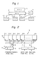
- Figure 1 is a schematic block diagram of a relatively large scale computer system using at least one main memory (main storage unit) having a plurality of memory banks.
- reference numerals 1-1 to 1-n designate a plurality of central processing units (CPU), 2-1 to 2-n a plurality of channel processing units (CHP), 3 a maintenance unit (MU), 4 a memory control unit (MCU), and 5 a main storage unit (MSU).
- CPU central processing units
- CHP channel processing units
- MU maintenance unit
- MCU memory control unit
- MSU main storage unit
- Each CHP 2 and CPU 1 is connected to the MSU 5 through the MCU 4.
- the MU 3 is connected directly to the MCU 4.
- the MCU 4 forms a queue by receiving requests for access to the MSU 5 transmitted from a CHP 2 or CPU 1, transfers the access requests to the MSU 5 in order based on the queue, and then transfers the read data from the MSU 5 to the CHP 2 or CPU 1 which requested access to the data.
- FIG. 2 is a conventional schematic structure of main storage unit (MSU) 5.
- the MSU 5 is constituted by an array section 10 having a plurality of memory banks 12-1 to 12-n and a control section 11 having an address register 13 and a command register 14. Each of the memory banks 12-1 to 12-n can independently write and read the data.
- a memory address is assigned to each of the memory banks 12-1 to 12-n by an interleaving method. That is, where there are eight bytes per one word, a byte address is assigned to each memory bank 12, i.e., memory bank 12-1 is "0”, memory bank 12-2 is “8", memory bank 12-3 is “16”, ... and memory bank 12-n is "8 x (n-1)", as shown in Fig. 2.
- the MCU 4 sets the memory address to be accessed to the address register 13 of the MSU 5, and sets the read or write command to the command register 14 of the MSU 5 based on the access request from, for example, the CPU 1.
- the MCU 4 simultaneously sets the data to be written to the write data register 15.
- the MSU 5 selects one of the memory banks 12 by a decoded output based on a part of contents of the register 13 in a decoder 19, and transfers the write data of the write data register 15 to a bank address register and a bank data register included in the memory bank 12. Accordingly, only one memory bank selected by the decoded output based on the content of the decoder 19 is operated by one access request.
- the data to be read from the selected memory bank 12 is set to a read data register 16, and transferred from the read data register 16 to the MCU 4.
- the operation for setting the memory address from the address register 13 to the bank address register in the memory bank 12 occupies at least one cycle, and, in general, the access operation in the memory bank 12 itself occupies several cycles. Accordingly, although the memory bank 12 under operation is occupied by the access operation during this time, another memory bank 12 can set the next memory address in order.
- the read or write data of one word per one cycle can be input to or output from the MSU 5 at a very high utilization efficiency.
- a more effective utilization i.e., an improvement of the practical throughput, has not yet been sufficiently achieved in a known memory access control system.
- a memory access control system according to an embodiment of the present invention will now be described.
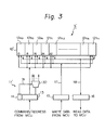
- FIG. 3 shows a schematic structure of a main storage unit (MSU) 5' according to an embodiment of the present invention.
- the main storage unit (MSU) 5' comprises an array section 10' divided into two groups of memory banks, i.e., even number memory banks (even banks) belonging to one group 12a0 to l2an,and odd number memory banks (odd banks) belonging to the other group 12b0 to l2bn, in accordance with whether the word address number is odd or even.
- Each memory address is assigned to each of the memory banks by an interleaving method as in the case of conventional memory banks.
- a two word access command is used to obtain access to the memory banks.
- the two word command comprises, for example, sixteen bytes (2 x eight bytes per one word) and can designate two memory banks by the access of two words constituted by a sequential address.
- a memory address and command sent from the memory control unit (MCU) are received by the address register 13 and the command register 14.
- the MSU 5' operates under the same procedure as for the conventional system.
- a decoder 30 selects one by one memory banks each having the sequential address alternately from the even bank group and the odd bank group. Accordingly, two memory banks from adjoining even and odd banks are selected by the decoder 30.
- an even bank having the even address is designated first by a head memory address of a so-called two words boundary (16 bytes boundary).
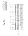
- Figures 4A to 4D are detailed block diagrams of the main storage unit shown in Fig. 3.
- even banks numbered 0, 2, 4, 6 ---, N-l correspond to the even banks 12a0, 12al, 12a2 ---12an shown in Fig. 3.
- odd banks 1, 3, 5 --- N correspond to the odd banks 12b0, l2bl, 12b2 --- l2bn shown in Fig. 3.
- Each memory bank whether even or odd, comprises a bank register constituted by an address register A, a write data register WD, and a read data register RD.
- Reference numerals 20 and 23 designate selectors (SEL). The selector 23 is used only for partial store data, and functions to merge partial store data with write data.
- the selector 20 has two functions, to merge the partial store data with the write data and to take an output timing of read data in correspondence with the output of a control pipeline 21a.
- Reference number 21 is a pipeline register consisting of a control pipeline (CTRL) 21a and a write data pipeline (WD) 21b.
- CTRL pipeline 21a controls the output timing of the read data by shifting the access request,.
- WD pipeline 21b controls the partial store data as explained below.
- Reference 22 designates means for generating an error correcting code (ECC).
- ECC error correcting code
- Reference numeral 30 is a decoder generating a "BANK GO" command to activate the selected memory bank based on the two word command sent from the command (CMD) register 14.
- FIGS 5A and 5B are timing charts of the operation in the command register 14, the address register 13, each of the memory banks, and the CTRL/WD pipelines 21a and 21b.
- a portion above the chain dotted line in the Figures is the memory control unit side.
- T 0 , T 1 , T 2 --- T 19 are access request timings for the operation of each register and memory bank. The period between each of the timings is equivalent to one access request cycle.
- the address register (MSU ADDR) 13 receives the memory address sent from the command/address register (MS CMD/ADDR) in the memory control unit (MCU) at the timing T 1 .
- the command register (MSU CMD) 14 also receives, for example, a two word command sent from the MS CMD/ADDR in the MCU at the timing T 1
- the write data register (MSU WDR) 15 also receives the write data sent from the write data register (MS WDR) in the MCU at the timing T l .
- the MSU CMD 14 sends the 16 bytes command to the decoder (DEC) 30.
- the decoder 30 generates the "BANK GO" command to the corresponding two memory banks selected, for example, EVEN BANK 0 and ODD BANK 1, and activates these banks.
- the bank address register A 0 in the EVEN BANK 0 and the bank address register A 1 in the ODD BANK 1 simultaneously receive the memory address, and the bank write data register WD 0 in the EVEN BANK 0 also receives the write data.
- the bank write data register WD 1 in the ODD BANK 1 receives the write data after a delay of one cycle, i.e., at the timing T 4 .
- the address register A 2 in the EVEN BANK 2 and the address register A3 in the ODD BANK 3 simultaneously receive the read address, and the read data register RD 2 in the EVEN BANK 2 reads out the stored data after eight cycles, i.e., at the timing T 12 , and this read out data is output from the read data register (MSU RDR) 16 through the ECC register 22.
- the read data register RD 3 in the ODD BANK 3 reads out the stored data after a delay of one cycle, i.e., at the timing T 13 .
- This read out control is performed by the control pipeline (CTRL) 21a.
- the command register (MS CMD) in the MCU can alternately command "write” and "read” instructions which consist of the two word command (FST 16 bytes and FCH 16 bytes; where FST is full store data and FCH is fetch data).
- the address register (MS ADDR) in the MCU sends commands to the address register (MSU ADDR) 13, and the MSU ADDR 13 designates two memory banks in the EVEN and ODD BANK's for both the "write” (store) and "read” (fetch) modes. Accordingly, at each timing, the MSU ADDR 13 can always activate two memory banks at every one cycle. These operations are performed similarly for other memory banks in the EVEN and ODD banks.
- the MSU ADDR 13 designates two memory banks in the EVEN and ODD BANK's based on a portion of the lower bank address, and the MSU WDR 15 sends the write data to the designated memory bank at the predetermined timing.
- the MSU WDR 15 and the MSU RDR 16 simultaneously hold data, i.e., the MSU WDR 15 holds the write data and the MSU RDR 16 holds the read data.
- the utilization efficiency, i.e., practical throughput, of the data bus lines 17 and 18 (up to) can be raised to a value of/a hundred percent as the maximum efficiency value.
- the CTRL pipeline 21a functions as a shift register.
- This pipeline 21a can shift the access request input from the MSU CMD 14 and the MSU RDR 13 by each pitch of P 1 , P 2 ---.
- shifting of the access request cycle 1 of the "MS GO" command in the MCU is started at the timing T 2 , at which the EVEN BANK 0 and the ODD BANK 1 are designated.
- shifting of the access request cycle 2 is started at the timing T 3 , at which the EVEN BANK 2 and the ODD BANK 3 are designated.
- the read data of the RD 2 of the EVEN BANK 2 is output to the MSU ADDR 16 by taking into account the correspondence between the read data and the shifted data in the selector (SEL) 20.
- the read data of the RD 3 of the ODD BANK 3 is output to the MSU ADDR 16.
- the CTRL pipe line 21a controls the output of the RD 3 so that it is delayed by only one access cycle, to enable the RD 3 to output the read data after a delay of one cycle of the output of the RD 2 .
- the read data of the RD 6 and the RD 7 are output by the same method as in the cycle 2.
- the WD pipeline 21b shown in Fig. 4C is used for changing the 8 bytes write data to, for example, 2 bytes write data, as partial store data.
- This pipeline 21b is activated by a "load access" sent from the MSU WDR 15.
- Two bus lines PL 1 and PL 2 are used for this operation. That is, the partial store data, for example, 2 bytes write data, is sent to the SEL 20 and merged with the 8 bytes read data. The merged 8 bytes write data is sent to the SEL 23 through the ECC 22.
- the ECC 22 provides a new error correcting code to the new 8 bytes write data.
- the output data of the SEL 23 is then written in the designated memory bank as the 8 bytes write data as explained above.
- FIGs 6A and 6B are detailed block diagrams of a memory control unit (MCU) 4' according to an embodiment of the present invention.
- MCU memory control unit
- FIG. 6B another main storage unit (MSU) 5" is connected to the MCU 4' through the bus line, and the central processing units (CPU 0, CPU 1) and the channel processing unit CHP are also connected to the MCU 4' through the bus line.
- the MCU 4' comprises, for example, two input ports PO and P1 for the address command sent from the address register MSAR in the CPU 0, two input ports PO and P1 for the CPU 1, and four channel ports PO , Pl , P2 , and P3 for the CHP.
- the MCU 4' also comprises write data ports corresponding to each CPU 0 port, CPU 1 port, and CHP port.
- the CPU 0 port WD is constituted by the ports POU and POL corresponding to the port PO , and the ports P1U and P1 L corresponding to the port P1.
- the port PO U is used for upper 8 bytes and the port POL for lower 8 bytes.
- each port PO , Pi , P 2 , and P 3 comprises a 16 bytes capacity, so that the CHP port WD comprises a 64 bytes (16 bytes x 4) capacity.
- Each port comprises a capacity of at least two words of data (for example, 8 bytes x 2), in this embodiment.
- a plurality of ports are provided in the MCU 4' corresponding to each CPU and CHP in order to raise the practical throughput of the MCU. These ports are provided because, since the practical throughput between the MSU and MCU is raised by using the above-explained division and control of the memory banks, it is necessary to raise the practical throughput between the MCU and CPU or CHP.
- a priority circuit 41 decides the priority of the address sent from each CPU 0, CPU 1 and CHP port, and sends the address selected by the priority decision to a write data selection register 42.
- the register 42 recognizes the corresponding port of the priority address selected by the priority circuit 41 and sends the corresponding write data to the MSU 5' or MSU 5" through a write data register MS WDR.
- the register 42 functions to select the two word command, i.e., 16 bytes per two cycles (the upper 8 bytes are always selected first, and then the lower 8 bytes are selected), or the one word command, i.e., 8 bytes per one cycle (in this case, only the upper 8 bytes are used).
- a BANK BUSY register 43 is used for storing a flag of the bank accessed by the priority circuit 4l,in order to control a next access "-designating the same memory bank as that the just previously accessed. This flag operation is used because, since the just previously accessed memory bank is "busy", when the same memory bank is designated again, the next access must be delayed for the predetermined term to avoid access collision.
- a pipeline 44 selects the fetch data read out from the MSU 5' and the MSU 5" by watching the read out timings of the MSU 5' and the MSU 5".
- the pipeline 44 also reports data transmission, completion of store and the like to the CPU and CHP.
- the selection between the MSU 5' and the MSU 5" is performed by the head address stored in each MSU and in the pipeline 44, in accordance with the correspondence between both head addresses.
- a store buffer SB comprises an address register ADDR, and write data registers WDU and WDL.
- the store buffer SB is used with a cache register (not shown).
- Each of the registers WDU and WDL comprise 8 bytes of upper data and 8 bytes of lower data, i.e., total ot 16 bytes of data per one address.
- the store buffer SB outputs a 16 bytes data access, i.e., two word access per two access cycles.
- 16 bytes data access is, in general, used whenever there is a data store access of more than 8 bytes, for example, a "move" command, or "store-multi" command.
- For a store access of an 8 bytes data only the upper 8 bytes are used for data access per one cycle.
- discrimination between the 16 byte data access and the 8 byte data access is based on the kind of command received (for example, "move”, “store-multi”, etc.) and the data length of the write data.
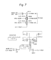
- Figures 7 and 8 show control circuits of the memory bank.
- the control circuit shown in Fig. 7 is provided at the input portion of each EVEN BANK, and the control circuit shown in Fig. 8 is provided at the input portion of each ODD BANK.
- the lower portion of the circuit is a three-bit counter as one embodiment.
- the flip-flop FF1 is used for the most significant bit, and the flip-flop FF3 is used for the least significant bit.
- An output OR gate OR2 always reaches a high level and outputs a clock hold signal CLK HOLD when the count is between "1" to "7".
- the signal CLK HOLD holds the contents of the registers when it is tuned ON. The input of the clock signal is inhibited while the CLK HOLD is turned ON.
- an operation code OPC WR provided to the head of the memory address indicates whether there is a one word command (8 bytes command) or two word command (16 bytes command). Accordingly, when the BANK GO and OPC WR are input to the flip-flop FFO through an AND gate, a write enable signal RAM WE having a high level signal is output directly from the flip-flop FFOto the memory bank (RAM).
- the lower portion of the circuit is a three-bit counter, as in the circuit shown in Fig. 7. Accordingly, a flip-flop FF1 is used for the most significant bit, and a flip-flop FF3 is used for the least significant bit.
- a write clock hold signal WR CLK HOLD is used equivalently as an address clock hold signal AD CLK HOLD and a write data clock signal WD CLK HOLD. In this case, the operation of this circuit is the same as that of the circuit shown in Fig. 7.
- the WD CLK HOLD signal is delayed by one cycle .from that of the WR CLK HOLD and receives the data at the second cycle.
- the AD CLK HOLD signal is longer by one cycle than that of the WR CLK HOLD, the AD CLK HOLD holds the address for an extra one cycle.
- operation code 16B indicates a 16 bytes access
- the 16 bytes access is input to the flip-flop FF
- the output timing of the write enable WE is delayed by only one cycle by using both AND gates and flip-flop circuit.
- the count becomes "7” the 16 bytes access is delayed by only one cycle by using the flip-flop FFO. Accordingly, the AD CLK HOLD is delayed by one cycle by output of the OR gate.
Landscapes
- Engineering & Computer Science (AREA)
- Theoretical Computer Science (AREA)
- Physics & Mathematics (AREA)
- General Engineering & Computer Science (AREA)
- General Physics & Mathematics (AREA)
- Dram (AREA)
- Memory System (AREA)
- Multi Processors (AREA)
- Memory System Of A Hierarchy Structure (AREA)
Applications Claiming Priority (2)
| Application Number | Priority Date | Filing Date | Title |
|---|---|---|---|
| JP59127805A JPS618785A (ja) | 1984-06-21 | 1984-06-21 | 記憶装置アクセス制御方式 |
| JP127805/84 | 1984-06-21 |
Publications (3)
| Publication Number | Publication Date |
|---|---|
| EP0165822A2 true EP0165822A2 (fr) | 1985-12-27 |
| EP0165822A3 EP0165822A3 (en) | 1989-02-22 |
| EP0165822B1 EP0165822B1 (fr) | 1994-06-08 |
Family
ID=14969111
Family Applications (1)
| Application Number | Title | Priority Date | Filing Date |
|---|---|---|---|
| EP85304442A Expired - Lifetime EP0165822B1 (fr) | 1984-06-21 | 1985-06-21 | Système de commande d'accès en mémoire |
Country Status (9)
| Country | Link |
|---|---|
| US (1) | US4866603A (fr) |
| EP (1) | EP0165822B1 (fr) |
| JP (1) | JPS618785A (fr) |
| KR (1) | KR910001448B1 (fr) |
| AU (1) | AU560427B2 (fr) |
| BR (1) | BR8502966A (fr) |
| CA (1) | CA1240069A (fr) |
| DE (1) | DE3587843T2 (fr) |
| ES (1) | ES8609770A1 (fr) |
Cited By (12)
| Publication number | Priority date | Publication date | Assignee | Title |
|---|---|---|---|---|
| WO1987004822A1 (fr) * | 1986-01-29 | 1987-08-13 | Digital Equipment Corporation | Procede et appareil d'adressage de matrices a semi-conducterus dans une unite de memoire centrale pendant des cycles d'horloges successifs du systeme |
| WO1989005488A3 (fr) * | 1987-12-11 | 1989-06-29 | Ncr Co | Systeme de memoire |
| GB2216307A (en) * | 1988-03-01 | 1989-10-04 | Ardent Computer Corp | Vector register file |
| EP0315550A3 (fr) * | 1987-11-06 | 1989-10-25 | Oryx Corporation | Architecture d'ordinateur hautement parallèle utilisant un commutateur à coordonnées avec retardement pipeline sélectable |
| FR2640402A1 (fr) * | 1988-12-08 | 1990-06-15 | Nec Corp | Dispositif de commande de memoire |
| EP0261751A3 (fr) * | 1986-09-25 | 1990-07-18 | Tektronix, Inc. | Système d'accès de mémoire concurrent |
| FR2653915A1 (fr) * | 1989-11-01 | 1991-05-03 | Nec Corp | Dispositif de controle de demandes d'acces a des blocs dans un systeme de traitement de donnees numeriques. |
| EP0380844A3 (fr) * | 1989-02-03 | 1992-01-02 | Digital Equipment Corporation | Méthode et dispositif d'interfaçage d'une unité de contrôle du système avec la mémoire centrale pour un système multiprocesseur |
| US5081575A (en) * | 1987-11-06 | 1992-01-14 | Oryx Corporation | Highly parallel computer architecture employing crossbar switch with selectable pipeline delay |
| ES2038928A2 (es) * | 1991-02-26 | 1993-08-01 | Fujitsu Ltd | Sistema de tratamiento de acceso en procesador de informacion. |
| DE10121745A1 (de) * | 2001-05-04 | 2002-11-14 | Systemonic Ag | Verfahren und Anordnung zu einem Stack mit einem, in Datengruppen mit mehreren Elementen aufgeteilten Speicher |
| DE102021107044A1 (de) | 2021-03-10 | 2022-09-15 | Elmos Semiconductor Se | Sicherheitsrelevantes Rechnersystems mit einem Datenspeicher und einem Datenspeicher |
Families Citing this family (37)
| Publication number | Priority date | Publication date | Assignee | Title |
|---|---|---|---|---|
| JP2895488B2 (ja) * | 1988-04-18 | 1999-05-24 | 株式会社東芝 | 半導体記憶装置及び半導体記憶システム |
| USRE39529E1 (en) * | 1988-04-18 | 2007-03-27 | Renesas Technology Corp. | Graphic processing apparatus utilizing improved data transfer to reduce memory size |
| KR930007185B1 (ko) * | 1989-01-13 | 1993-07-31 | 가부시키가이샤 도시바 | 레지스터뱅크회로 |
| JPH0740241B2 (ja) * | 1989-01-17 | 1995-05-01 | 富士通株式会社 | リクエストキャンセル方式 |
| JPH0775006B2 (ja) * | 1989-03-16 | 1995-08-09 | 株式会社日立製作所 | 記憶装置の制御方法 |
| US5091851A (en) * | 1989-07-19 | 1992-02-25 | Hewlett-Packard Company | Fast multiple-word accesses from a multi-way set-associative cache memory |
| DE69122520T2 (de) * | 1990-01-31 | 1997-02-13 | Hewlett Packard Co | Vielfachbus-Systemspeicherarchitektur |
| JP3215105B2 (ja) * | 1990-08-24 | 2001-10-02 | 富士通株式会社 | メモリアクセス装置 |
| GB9018990D0 (en) * | 1990-08-31 | 1990-10-17 | Ncr Co | Register control for workstation interfacing means |
| US5303309A (en) * | 1990-09-18 | 1994-04-12 | E-Mu Systems, Inc. | Digital sampling instrument |
| US5289584A (en) * | 1991-06-21 | 1994-02-22 | Compaq Computer Corp. | Memory system with FIFO data input |
| EP0615190A1 (fr) * | 1993-03-11 | 1994-09-14 | Data General Corporation | Mémoire extensible pour un ordinateur numérique |
| TW357295B (en) * | 1994-02-08 | 1999-05-01 | United Microelectronics Corp | Microprocessor's data writing, reading operations |
| US6301299B1 (en) * | 1994-10-28 | 2001-10-09 | Matsushita Electric Industrial Co., Ltd. | Memory controller for an ATSC video decoder |
| US5644780A (en) * | 1995-06-02 | 1997-07-01 | International Business Machines Corporation | Multiple port high speed register file with interleaved write ports for use with very long instruction word (vlin) and n-way superscaler processors |
| FR2748595B1 (fr) * | 1996-05-10 | 1998-07-10 | Sgs Thomson Microelectronics | Memoire a acces parallele |
| US6026473A (en) * | 1996-12-23 | 2000-02-15 | Intel Corporation | Method and apparatus for storing data in a sequentially written memory using an interleaving mechanism |
| US5959929A (en) * | 1997-12-29 | 1999-09-28 | Micron Technology, Inc. | Method for writing to multiple banks of a memory device |
| KR100313503B1 (ko) * | 1999-02-12 | 2001-11-07 | 김영환 | 멀티-뱅크 메모리 어레이를 갖는 반도체 메모리 장치 |
| KR100328726B1 (ko) * | 1999-04-29 | 2002-03-20 | 한탁돈 | 메모리 엑세스 시스템 및 그 제어방법 |
| US6377502B1 (en) * | 1999-05-10 | 2002-04-23 | Kabushiki Kaisha Toshiba | Semiconductor device that enables simultaneous read and write/erase operation |
| US6438024B1 (en) * | 2001-01-11 | 2002-08-20 | Sun Microsystems, Inc. | Combining RAM and ROM into a single memory array |
| US6839797B2 (en) | 2001-12-21 | 2005-01-04 | Agere Systems, Inc. | Multi-bank scheduling to improve performance on tree accesses in a DRAM based random access memory subsystem |
| US8250295B2 (en) * | 2004-01-05 | 2012-08-21 | Smart Modular Technologies, Inc. | Multi-rank memory module that emulates a memory module having a different number of ranks |
| US7289386B2 (en) * | 2004-03-05 | 2007-10-30 | Netlist, Inc. | Memory module decoder |
| US7532537B2 (en) * | 2004-03-05 | 2009-05-12 | Netlist, Inc. | Memory module with a circuit providing load isolation and memory domain translation |
| US7916574B1 (en) | 2004-03-05 | 2011-03-29 | Netlist, Inc. | Circuit providing load isolation and memory domain translation for memory module |
| US8595459B2 (en) * | 2004-11-29 | 2013-11-26 | Rambus Inc. | Micro-threaded memory |
| US20060277355A1 (en) * | 2005-06-01 | 2006-12-07 | Mark Ellsberry | Capacity-expanding memory device |
| EP2071468A4 (fr) | 2006-12-25 | 2010-11-03 | Panasonic Corp | Dispositif de commande de mémoire, dispositif de mémoire et procédé de commande de mémoire |
| US8417870B2 (en) | 2009-07-16 | 2013-04-09 | Netlist, Inc. | System and method of increasing addressable memory space on a memory board |
| US8154901B1 (en) | 2008-04-14 | 2012-04-10 | Netlist, Inc. | Circuit providing load isolation and noise reduction |
| US8516185B2 (en) | 2009-07-16 | 2013-08-20 | Netlist, Inc. | System and method utilizing distributed byte-wise buffers on a memory module |
| US9128632B2 (en) | 2009-07-16 | 2015-09-08 | Netlist, Inc. | Memory module with distributed data buffers and method of operation |
| KR101292309B1 (ko) * | 2011-12-27 | 2013-07-31 | 숭실대학교산학협력단 | 반도체칩 및 메모리 제어방법, 그리고 그 방법을 컴퓨터에서 실행시키기 위한 프로그램을 기록한 기록매체 |
| PL3629123T3 (pl) | 2013-07-27 | 2021-08-16 | Netlist, Inc. | Moduł pamięci z lokalną synchronizacją |
| WO2019134028A1 (fr) | 2018-01-02 | 2019-07-11 | Reed Scientific Services Ltd. | Système de rhizosphère à écoulement continu à base de terre pour le traitement d'eau et de sol contaminés |
Family Cites Families (17)
| Publication number | Priority date | Publication date | Assignee | Title |
|---|---|---|---|---|
| BE755034A (fr) * | 1969-08-19 | 1971-02-19 | Siemens Ag | Installation de traitement d'informations a commande centrale programmepar memoire |
| JPS5410219B2 (fr) * | 1973-12-07 | 1979-05-02 | ||
| US4099231A (en) * | 1975-10-01 | 1978-07-04 | Digital Equipment Corporation | Memory control system for transferring selected words in a multiple memory word exchange during one memory cycle |
| JPS5475941A (en) * | 1977-11-30 | 1979-06-18 | Fujitsu Ltd | Control system for memory unit |
| US4298929A (en) * | 1979-01-26 | 1981-11-03 | International Business Machines Corporation | Integrated multilevel storage hierarchy for a data processing system with improved channel to memory write capability |
| US4317168A (en) * | 1979-11-23 | 1982-02-23 | International Business Machines Corporation | Cache organization enabling concurrent line castout and line fetch transfers with main storage |
| JPS5736353A (ja) * | 1980-08-13 | 1982-02-27 | Toshiba Corp | Memoriakusesuhoshiki |
| JPS57105879A (en) * | 1980-12-23 | 1982-07-01 | Hitachi Ltd | Control system for storage device |
| JPS57113165A (en) * | 1980-12-29 | 1982-07-14 | Fujitsu Ltd | Data processor |
| US4438493A (en) * | 1981-07-06 | 1984-03-20 | Honeywell Information Systems Inc. | Multiwork memory data storage and addressing technique and apparatus |
| US4439827A (en) * | 1981-12-28 | 1984-03-27 | Raytheon Company | Dual fetch microsequencer |
| JPS58149548A (ja) * | 1982-03-02 | 1983-09-05 | Hitachi Ltd | メモリ制御方式 |
| US4513372A (en) * | 1982-11-15 | 1985-04-23 | Data General Corporation | Universal memory |
| JPS6015771A (ja) * | 1983-07-08 | 1985-01-26 | Hitachi Ltd | ベクトルプロセッサ |
| JPS60157646A (ja) * | 1984-01-27 | 1985-08-17 | Mitsubishi Electric Corp | メモリバンク切換装置 |
| JPH0670773B2 (ja) * | 1984-11-01 | 1994-09-07 | 富士通株式会社 | 先行制御方式 |
| JPS62194561A (ja) * | 1986-02-21 | 1987-08-27 | Toshiba Corp | 半導体記憶装置 |
-
1984
- 1984-06-21 JP JP59127805A patent/JPS618785A/ja active Granted
-
1985
- 1985-06-14 CA CA000484012A patent/CA1240069A/fr not_active Expired
- 1985-06-17 AU AU43733/85A patent/AU560427B2/en not_active Ceased
- 1985-06-20 BR BR8502966A patent/BR8502966A/pt not_active IP Right Cessation
- 1985-06-20 ES ES544377A patent/ES8609770A1/es not_active Expired
- 1985-06-20 KR KR1019850004386A patent/KR910001448B1/ko not_active Expired
- 1985-06-21 EP EP85304442A patent/EP0165822B1/fr not_active Expired - Lifetime
- 1985-06-21 DE DE3587843T patent/DE3587843T2/de not_active Expired - Fee Related
-
1988
- 1988-01-20 US US07/147,071 patent/US4866603A/en not_active Expired - Lifetime
Cited By (18)
| Publication number | Priority date | Publication date | Assignee | Title |
|---|---|---|---|---|
| US4791552A (en) * | 1986-01-29 | 1988-12-13 | Digital Equipment Corporation | Apparatus and method for addressing semiconductor arrays in a main memory unit on consecutive system clock cycles |
| WO1987004822A1 (fr) * | 1986-01-29 | 1987-08-13 | Digital Equipment Corporation | Procede et appareil d'adressage de matrices a semi-conducterus dans une unite de memoire centrale pendant des cycles d'horloges successifs du systeme |
| EP0261751A3 (fr) * | 1986-09-25 | 1990-07-18 | Tektronix, Inc. | Système d'accès de mémoire concurrent |
| US5081575A (en) * | 1987-11-06 | 1992-01-14 | Oryx Corporation | Highly parallel computer architecture employing crossbar switch with selectable pipeline delay |
| EP0315550A3 (fr) * | 1987-11-06 | 1989-10-25 | Oryx Corporation | Architecture d'ordinateur hautement parallèle utilisant un commutateur à coordonnées avec retardement pipeline sélectable |
| WO1989005488A3 (fr) * | 1987-12-11 | 1989-06-29 | Ncr Co | Systeme de memoire |
| GB2216307A (en) * | 1988-03-01 | 1989-10-04 | Ardent Computer Corp | Vector register file |
| GB2216307B (en) * | 1988-03-01 | 1992-08-26 | Ardent Computer Corp | Vector register file |
| FR2640402A1 (fr) * | 1988-12-08 | 1990-06-15 | Nec Corp | Dispositif de commande de memoire |
| EP0380844A3 (fr) * | 1989-02-03 | 1992-01-02 | Digital Equipment Corporation | Méthode et dispositif d'interfaçage d'une unité de contrôle du système avec la mémoire centrale pour un système multiprocesseur |
| FR2653915A1 (fr) * | 1989-11-01 | 1991-05-03 | Nec Corp | Dispositif de controle de demandes d'acces a des blocs dans un systeme de traitement de donnees numeriques. |
| ES2038928A2 (es) * | 1991-02-26 | 1993-08-01 | Fujitsu Ltd | Sistema de tratamiento de acceso en procesador de informacion. |
| DE10121745A1 (de) * | 2001-05-04 | 2002-11-14 | Systemonic Ag | Verfahren und Anordnung zu einem Stack mit einem, in Datengruppen mit mehreren Elementen aufgeteilten Speicher |
| US6871256B2 (en) | 2001-05-04 | 2005-03-22 | Systemonic Ag | Method and arrangement in a stack having a memory segmented into data groups having a plurality of elements |
| DE102021107044A1 (de) | 2021-03-10 | 2022-09-15 | Elmos Semiconductor Se | Sicherheitsrelevantes Rechnersystems mit einem Datenspeicher und einem Datenspeicher |
| DE102021107045A1 (de) | 2021-03-10 | 2022-09-15 | Elmos Semiconductor Se | Rechnersystem für eine Motorsteuerung mit einem Programmspeicher und einem Datenspeicher |
| DE102021107045B4 (de) | 2021-03-10 | 2024-11-21 | Elmos Semiconductor Se | Rechnersystem für eine Motorsteuerung mit einem Programmspeicher und einem Datenspeicher |
| DE102021107044B4 (de) | 2021-03-10 | 2024-11-21 | Elmos Semiconductor Se | Sicherheitsrelevantes Rechnersystems mit einem Programmspeicher und einem Datenspeicher |
Also Published As
| Publication number | Publication date |
|---|---|
| JPH0363096B2 (fr) | 1991-09-30 |
| DE3587843T2 (de) | 1994-09-15 |
| EP0165822B1 (fr) | 1994-06-08 |
| ES544377A0 (es) | 1986-07-16 |
| CA1240069A (fr) | 1988-08-02 |
| JPS618785A (ja) | 1986-01-16 |
| KR860000601A (ko) | 1986-01-29 |
| AU560427B2 (en) | 1987-04-09 |
| ES8609770A1 (es) | 1986-07-16 |
| DE3587843D1 (de) | 1994-07-14 |
| EP0165822A3 (en) | 1989-02-22 |
| AU4373385A (en) | 1986-01-02 |
| US4866603A (en) | 1989-09-12 |
| KR910001448B1 (ko) | 1991-03-07 |
| BR8502966A (pt) | 1986-03-04 |
Similar Documents
| Publication | Publication Date | Title |
|---|---|---|
| EP0165822A2 (fr) | Système de commande d'accès en mémoire | |
| EP0100943B1 (fr) | Système de mémoire hièrarchique | |
| US4930066A (en) | Multiport memory system | |
| US5479635A (en) | Memory device including DRAMs for high-speed accessing | |
| EP0054888B1 (fr) | Système de traitement de données à commande de mémoire principale et de mémoire tampon | |
| CA1089107A (fr) | Controleur de bus de canal | |
| EP0126976A2 (fr) | Système de multiprocesseur avec mémoire partagée à accès aléatoire pour l'intercommunication | |
| US3931613A (en) | Data processing system | |
| EP0180237A2 (fr) | Système de traitement de données avec commande à précision | |
| US6223253B1 (en) | Word selection logic to implement an 80 or 96-bit cache SRAM | |
| JPH0756815A (ja) | キャッシュ動作方法及びキャッシュ | |
| KR880001171B1 (ko) | 순차적인 워어드가 정열된 어드레스 지정장치 | |
| US5138705A (en) | Chip organization for an extendable memory structure providing busless internal page transfers | |
| US4718039A (en) | Intermediate memory array with a parallel port and a buffered serial port | |
| US4796222A (en) | Memory structure for nonsequential storage of block bytes in multi-bit chips | |
| US6266796B1 (en) | Data ordering for cache data transfer | |
| EP0437160B1 (fr) | Cartes mémoires principales ne comprenant qu'un seul bit de fonction de positionnement et de remise à l'état initial | |
| US7436728B2 (en) | Fast random access DRAM management method including a method of comparing the address and suspending and storing requests | |
| US4992979A (en) | Memory structure for nonsequential storage of block bytes in multi bit chips | |
| US5627991A (en) | Cache memory having a multiplexor assembly for ordering output on a data chunk basis | |
| EP0473804A1 (fr) | Alignement des élements de ligne pour transfert de données de la mémoire vers le cache | |
| US4493030A (en) | Plural data processor groups controlling a telecommunications exchange | |
| US5822766A (en) | Main memory interface for high speed data transfer | |
| JP2636485B2 (ja) | キャッシュ記憶装置 | |
| EP0446002B1 (fr) | Mémoire à l'échelle d'une tranche à accès multibit et système de mémoire à l'échelle d'une tranche |
Legal Events
| Date | Code | Title | Description |
|---|---|---|---|
| PUAI | Public reference made under article 153(3) epc to a published international application that has entered the european phase |
Free format text: ORIGINAL CODE: 0009012 |
|
| AK | Designated contracting states |
Designated state(s): DE FR GB |
|
| PUAL | Search report despatched |
Free format text: ORIGINAL CODE: 0009013 |
|
| AK | Designated contracting states |
Kind code of ref document: A3 Designated state(s): DE FR GB |
|
| 17P | Request for examination filed |
Effective date: 19890503 |
|
| 17Q | First examination report despatched |
Effective date: 19901026 |
|
| GRAA | (expected) grant |
Free format text: ORIGINAL CODE: 0009210 |
|
| AK | Designated contracting states |
Kind code of ref document: B1 Designated state(s): DE FR GB |
|
| REF | Corresponds to: |
Ref document number: 3587843 Country of ref document: DE Date of ref document: 19940714 |
|
| ET | Fr: translation filed | ||
| PLBE | No opposition filed within time limit |
Free format text: ORIGINAL CODE: 0009261 |
|
| STAA | Information on the status of an ep patent application or granted ep patent |
Free format text: STATUS: NO OPPOSITION FILED WITHIN TIME LIMIT |
|
| 26N | No opposition filed | ||
| PGFP | Annual fee paid to national office [announced via postgrant information from national office to epo] |
Ref country code: FR Payment date: 20010611 Year of fee payment: 17 Ref country code: DE Payment date: 20010611 Year of fee payment: 17 |
|
| PGFP | Annual fee paid to national office [announced via postgrant information from national office to epo] |
Ref country code: GB Payment date: 20010620 Year of fee payment: 17 |
|
| REG | Reference to a national code |
Ref country code: GB Ref legal event code: IF02 |
|
| PG25 | Lapsed in a contracting state [announced via postgrant information from national office to epo] |
Ref country code: GB Free format text: LAPSE BECAUSE OF NON-PAYMENT OF DUE FEES Effective date: 20020621 |
|
| PG25 | Lapsed in a contracting state [announced via postgrant information from national office to epo] |
Ref country code: DE Free format text: LAPSE BECAUSE OF NON-PAYMENT OF DUE FEES Effective date: 20030101 |
|
| GBPC | Gb: european patent ceased through non-payment of renewal fee |
Effective date: 20020621 |
|
| PG25 | Lapsed in a contracting state [announced via postgrant information from national office to epo] |
Ref country code: FR Free format text: LAPSE BECAUSE OF NON-PAYMENT OF DUE FEES Effective date: 20030228 |
|
| REG | Reference to a national code |
Ref country code: FR Ref legal event code: ST |