EP0166948A2 - Dispositifs d'affichage et sous-ensembles avec électrodes pour les éléments d'image - Google Patents
Dispositifs d'affichage et sous-ensembles avec électrodes pour les éléments d'image Download PDFInfo
- Publication number
- EP0166948A2 EP0166948A2 EP85106404A EP85106404A EP0166948A2 EP 0166948 A2 EP0166948 A2 EP 0166948A2 EP 85106404 A EP85106404 A EP 85106404A EP 85106404 A EP85106404 A EP 85106404A EP 0166948 A2 EP0166948 A2 EP 0166948A2
- Authority
- EP
- European Patent Office
- Prior art keywords
- display
- further characterized
- electrode
- isolation
- pixel
- Prior art date
- Legal status (The legal status is an assumption and is not a legal conclusion. Google has not performed a legal analysis and makes no representation as to the accuracy of the status listed.)
- Granted
Links
Images


Classifications
-
- G—PHYSICS
- G02—OPTICS
- G02F—OPTICAL DEVICES OR ARRANGEMENTS FOR THE CONTROL OF LIGHT BY MODIFICATION OF THE OPTICAL PROPERTIES OF THE MEDIA OF THE ELEMENTS INVOLVED THEREIN; NON-LINEAR OPTICS; FREQUENCY-CHANGING OF LIGHT; OPTICAL LOGIC ELEMENTS; OPTICAL ANALOGUE/DIGITAL CONVERTERS
- G02F1/00—Devices or arrangements for the control of the intensity, colour, phase, polarisation or direction of light arriving from an independent light source, e.g. switching, gating or modulating; Non-linear optics
- G02F1/01—Devices or arrangements for the control of the intensity, colour, phase, polarisation or direction of light arriving from an independent light source, e.g. switching, gating or modulating; Non-linear optics for the control of the intensity, phase, polarisation or colour
- G02F1/13—Devices or arrangements for the control of the intensity, colour, phase, polarisation or direction of light arriving from an independent light source, e.g. switching, gating or modulating; Non-linear optics for the control of the intensity, phase, polarisation or colour based on liquid crystals, e.g. single liquid crystal display cells
- G02F1/133—Constructional arrangements; Operation of liquid crystal cells; Circuit arrangements
- G02F1/136—Liquid crystal cells structurally associated with a semi-conducting layer or substrate, e.g. cells forming part of an integrated circuit
- G02F1/1362—Active matrix addressed cells
- G02F1/13624—Active matrix addressed cells having more than one switching element per pixel
-
- G—PHYSICS
- G02—OPTICS
- G02F—OPTICAL DEVICES OR ARRANGEMENTS FOR THE CONTROL OF LIGHT BY MODIFICATION OF THE OPTICAL PROPERTIES OF THE MEDIA OF THE ELEMENTS INVOLVED THEREIN; NON-LINEAR OPTICS; FREQUENCY-CHANGING OF LIGHT; OPTICAL LOGIC ELEMENTS; OPTICAL ANALOGUE/DIGITAL CONVERTERS
- G02F1/00—Devices or arrangements for the control of the intensity, colour, phase, polarisation or direction of light arriving from an independent light source, e.g. switching, gating or modulating; Non-linear optics
- G02F1/01—Devices or arrangements for the control of the intensity, colour, phase, polarisation or direction of light arriving from an independent light source, e.g. switching, gating or modulating; Non-linear optics for the control of the intensity, phase, polarisation or colour
- G02F1/13—Devices or arrangements for the control of the intensity, colour, phase, polarisation or direction of light arriving from an independent light source, e.g. switching, gating or modulating; Non-linear optics for the control of the intensity, phase, polarisation or colour based on liquid crystals, e.g. single liquid crystal display cells
- G02F1/133—Constructional arrangements; Operation of liquid crystal cells; Circuit arrangements
- G02F1/1333—Constructional arrangements; Manufacturing methods
- G02F1/1343—Electrodes
- G02F1/134309—Electrodes characterised by their geometrical arrangement
- G02F1/134336—Matrix
-
- G—PHYSICS
- G02—OPTICS
- G02F—OPTICAL DEVICES OR ARRANGEMENTS FOR THE CONTROL OF LIGHT BY MODIFICATION OF THE OPTICAL PROPERTIES OF THE MEDIA OF THE ELEMENTS INVOLVED THEREIN; NON-LINEAR OPTICS; FREQUENCY-CHANGING OF LIGHT; OPTICAL LOGIC ELEMENTS; OPTICAL ANALOGUE/DIGITAL CONVERTERS
- G02F1/00—Devices or arrangements for the control of the intensity, colour, phase, polarisation or direction of light arriving from an independent light source, e.g. switching, gating or modulating; Non-linear optics
- G02F1/01—Devices or arrangements for the control of the intensity, colour, phase, polarisation or direction of light arriving from an independent light source, e.g. switching, gating or modulating; Non-linear optics for the control of the intensity, phase, polarisation or colour
- G02F1/13—Devices or arrangements for the control of the intensity, colour, phase, polarisation or direction of light arriving from an independent light source, e.g. switching, gating or modulating; Non-linear optics for the control of the intensity, phase, polarisation or colour based on liquid crystals, e.g. single liquid crystal display cells
- G02F1/133—Constructional arrangements; Operation of liquid crystal cells; Circuit arrangements
- G02F1/1333—Constructional arrangements; Manufacturing methods
- G02F1/1343—Electrodes
- G02F1/134309—Electrodes characterised by their geometrical arrangement
- G02F1/134345—Subdivided pixels, e.g. for grey scale or redundancy
-
- G—PHYSICS
- G02—OPTICS
- G02F—OPTICAL DEVICES OR ARRANGEMENTS FOR THE CONTROL OF LIGHT BY MODIFICATION OF THE OPTICAL PROPERTIES OF THE MEDIA OF THE ELEMENTS INVOLVED THEREIN; NON-LINEAR OPTICS; FREQUENCY-CHANGING OF LIGHT; OPTICAL LOGIC ELEMENTS; OPTICAL ANALOGUE/DIGITAL CONVERTERS
- G02F1/00—Devices or arrangements for the control of the intensity, colour, phase, polarisation or direction of light arriving from an independent light source, e.g. switching, gating or modulating; Non-linear optics
- G02F1/01—Devices or arrangements for the control of the intensity, colour, phase, polarisation or direction of light arriving from an independent light source, e.g. switching, gating or modulating; Non-linear optics for the control of the intensity, phase, polarisation or colour
- G02F1/13—Devices or arrangements for the control of the intensity, colour, phase, polarisation or direction of light arriving from an independent light source, e.g. switching, gating or modulating; Non-linear optics for the control of the intensity, phase, polarisation or colour based on liquid crystals, e.g. single liquid crystal display cells
- G02F1/133—Constructional arrangements; Operation of liquid crystal cells; Circuit arrangements
- G02F1/136—Liquid crystal cells structurally associated with a semi-conducting layer or substrate, e.g. cells forming part of an integrated circuit
- G02F1/1362—Active matrix addressed cells
- G02F1/1365—Active matrix addressed cells in which the switching element is a two-electrode device
Definitions
- the present invention relates generally to light influencing displays and more particularly to light influencing display subassemblies and display.
- light influencing displays find use in digital watches, digital clocks, calculators, pocket sized television receivers, and various forms of portable games, to name just a few.
- Light influencing displays can be formed in many configurations.
- light influencing material any material which emits light or can be used to selectively vary the intensity, phase, or polarization of light either being reflected from or transmitted through the material.
- Liquid crystal material is only one such material having these characteristics.
- each pixel includes a pair of electrodes which can be individally addressable. As is well known, when a voltage is applied across the electrodes, the optical properties of the light influencing material can be changed to provide a lighter or darker display depending upon the type of material used and the desired mode of operation of the display.
- An increasingly important type of light influencing display matrix includes a large number of pixel elements arranged in rows and columns. Because of the large number of pixels in the matrix arrays, the electrode line connections to each pixel are on common lines with other pixels. In this so-called multiplexing scheme, each pixel is located at a unique intersection of two address lines. Each pixel is individually addressed by applying a voltage potential across its two intersecting lines.
- isolation is meant any device which enhances the ability for one pixel to be addressed (switched) without switching other pixels on a common address line.
- isolation devices are single polarity devices, which can be turned on in only one direction or polarity, while others are dual polarity devices, which can be turned on in two directions or polarities.
- the individual pixel structures in prior light influencing displays result in lower frequency operation, more complex electronic circuitry, less flexibility, reduced yield and less isolation than desired.
- the prior circuits often have the pixel isolation devices, one address line and one electrode on one substrate or plane and the other electrode and address line on the other plane.
- the display material and the two electrodes form a capacitor which limits the operational frequency.
- the electronic circuitry is more complex than desired and limits the flexibility of the displays, since both planes have circuitry thereon. Where there is no redundancy in the pixel isolation devices, any one inoperative device will cause an inoperative pixel element reducing the display yield.
- the prior display pixels in attempting to reduce the circuitry on both planes generally are limited to a pair of electrodes with the isolation device or devices only on one plane and coupled to only one electrode address line on that plane.
- the present invention provides a display of the type having a structure in which all of the electronic circuitry, including isolation devices where utilized, is located at one electrode side of each pixel electrode combination.
- the structure includes the subdivision of one pixel electrode into at least two spaced apart side-by-side electrode segments on one plane opposite one common electrode on a second plane for each pixel.
- Light influencing material is disposed between the electrode segments and the common electrode.
- the segmented electrode can increase the operational frequency while decreasing the electronic complexity of the display.
- the address lines can be coupled to each segmented electrode by one or more isolation devices to provide more complete pixel isolation and to increase the manufacturing yield of the displays.
- the present invention provides a display including at least one pixel element.
- the pixel element is formed with a segmented electrode including at least a pair of spaced apart electrode segments, a common electrode spaced from the segmented electrode in substantially parallel relation thereto, with light influencing material between the segmented electrode and the common electrode.
- At least one isolation device can be coupled to the electrode segments and a pair of isolation devices preferably can be coupled to the electrode segments.
- the isolation devices can be diodes which can be formed from a deposited semiconductor material.
- the deposited semiconductor material is preferably an amorphous semiconductor alloy including silicon.
- the diodes preferably include a first doped semiconductor region, a substantially intrinsic semiconductor region overlying the first doped region, and a second doped semiconductor region opposite in conductivity with respect to the first doped region overlying the intrinsic region.
- the present invention further provides a display subassembly, which display includes at least one pixel element.
- the subassembly includes a substrate, a segmented electrode including at least a pair of spaced apart electrode segments formed on the substrate and at least one address line coupled to each of the electrode segments.
- the subassembly can include isolation devices coupling one or both lines to the electrode segments and formed on the same plane or substrate.
- the display subassembly can then have light influencing display material applied between at least the segmented electrode and the common electrode to form a completed display.
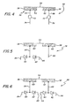
- the liquid crystal display 10 includes a pair of pixels 12 and 14.
- the liquid crystal display 10 can include a first common x addressing line 16 which is coupled through the pixels 12 and 14 to respective y addressing lines 18 and 20.
- the x addressing line 16 is generally formed on one plane or substrate (not illustrated) and is coupled to a first electrode 22 and 24 of the pixels 12 and 14.
- the y addressing lines 18 and 20 are generally formed on a second plane or substrate (not illustrated) and are coupled to a respective second electrode 26 and 28.
- a liquid crystal display material 30 is applied between the electrodes 22 and 26, 24 and 28, which effectively forms a capacitor with the electrodes.
- the pixels 12 and 14 can also include separate x addressing lines.
- a schematic diagram of an improved light influencing display pixel 32 is best illustrated.
- the pixel 32 is fully disclosed in U.S. Patent Application Serial No. 573,004, entitled “Liquid Crystal Displays Operated By Amorphous Silicon Alloy Diodes", filed in the names of Zvi Yaniv, Vincent D. Cannella, Gregory L. Hansell 1 and Louis D. Schwartz, on January 23, 1984, which is incorporated herein by reference.
- the pixel 32 includes a first x addressing line 34 which is coupled through the pixel to a y addressing line 36.
- the addressing line 34 is generally formed on one plane or substrate (not illustrated) and is coupled to a first electrode 38.
- the y addressing line 36 is generally formed on a second plane or substrate (not illustrated) and is coupled to a second electrode 40.
- a light influencing material such as liquid crystal display material 42 is applied between the electrodes 38 and 40, which again effectively forms a capacitor.
- light influencing material is meant any material which emits light or can be used to selectively vary the intensity, phase, or polarization of light either being reflected from or transmitted through the material. Liquid crystal material being one such material having these characteristics.
- the y addressing line 36 typically includes at least one dual polarity isolation device, such as a tr d nsistor (not illustrated) or a pair of single polarity isolation devices 44 and 46. Each of the devices 44 and 46 has a respective address line 48 ' and 50, respectively.
- the devices 44 and 46 are illustrated as diodes for simplicity, but can be any type of single polarity isolation device. Again, as above mentioned, by the term “isolation device” is meant any device which enhances the ability for one pixel to be addressed (switched) without switching other pixels on a common address line.
- the useful life of a nematic liquid crystal display material can be extended if the polarity of the applied voltage potential is periodically reversed, such as during alternate display frames. This can be accomplished, for example, with the pixel 32 by applying a positive potential on line 48 and a negative potential on line 34 during one frame or time period to forward bias the diode 44 and effectively charge the capacitor in one polarity. The next time perioo or frame, a positive potential is applied to the line 34 and a negative potential is applied to the line 50 to forward bias the diode 46. Repeating this sequence causes the potential applied to the capacitor and hence the liquid crystal display material 42 to be reversed during alternate frames. The switching speed or frequency is limited by the time it takes to charge the capacitor.
- the pixels 12, 14 and 32 require that electronic circuitry be formed on both planes which requires connectors to both planes on opposite sides of the liquid crystal display material.
- the operating frequency is limited by the capacitor formed by the pixel electrodes and the liquid crystal display material.
- Full isolation for the pixels can only be accomplished by adding isolation devices to the x addressing line 16 or 34, further complicating the circuitry on the second plane. Also, no redundancy is provided for the isolation devices 44 and 46 and if one is defective the pixel 32, and hence the display, will be defective.
- just one pixel element is illustrated in the Figs., it can be appreciated that many such pixels can be formed in for example, a row and column arrangement to provide a complete liquid crystal display of any size.
- Fig. 3 illustrates a first pixel embodiment 52 of the invention.
- the pixel 52 includes a common electrode 54 having at least one electrode segment on one plane (not illustrated) separated from a second segmented electrode 56 on a second plane (not illustrated) by a light influencing material, such as liquid crystal display material 58.
- the segmented electrode 56 is subdivided into at least a pair of spaced apart electrode segments 60 and 62 coupled to separate respective x and y address lines 64 and 66.
- the electrode segments 60 and 62 provide the pixel 52 with a number of advantages over the pixels 12, 14 and 32. All the electronic circuitry can be formed on the same plane with the electrode segments 60 and 62.
- the common electrode 54 on the opposite plane can merely be a floating electrode with no pixel addressing circuitry connected to it.
- the electrode segments 60 and 62, the liquid crystal display material 58 and the common electrode 54 result in a capacitor with one-quarter of the capacitance of the above described capacitors. Assuming the liquid crystal display material is the same, and the electrode spacing is the same, then the result is two capacitors, each equivalent to one-half the prior capacitors, in series. These two capacitors in series result in one-quarter the capacitance which requires twice the voltage, but one-half the charge to obtain the same field. Thus, utilizing the same current, the frequency is doubled.
- the applied voltage potential should be reversed periodically, such as the beginning of each frame. This can be accomplished by applying a positive potential on line 64 and a negative potential on line 66 in the first time frame. In the next time frame, a positive potential is applied to the line 66 and a negative potential to the line 64 to reverse the applied voltage potential. This sequence is repeated to enhance the lifetime of the liquid crystal display material.
- Fig. 4 illustrates a second pixel embodiment 68 of the invention with elements corresponding to the elements in the pixel 52 having the same numerals.
- the pixel 68 includes a pair of dual polarity isolation devices 70 and 72 coupled to respective address lines 64 and 66 and to address lines 74 and 76. Although one isolation device is illustrated coupled to each of the electrode segments 60 and 62, since the devices are dual polarity only one of the electrode segments needs to be coupled to an isolation device.
- the second isolation device adds redundancy to the pixel 68, since the pixel 68 will operate with one of the isolation devices shorted.
- the applied voltage potential can be reversed as previously described, by alternating the polarity of the one or two isolation devices along with the applied potentials.
- Fig. 5 illustrates another pixel embodiment 78 of the invention, again utilizing numerals corresponding to the pixel 52 where applicable.
- the electrode segment 60 and the addressing line 64 are coupled through a pair of isolation devices 80 and 82 which are coupled to separate respective lines 84 and 86.
- a positive potential is applied to the line 84 and a negative potential to the line 66 to forward bias the diode 80.
- a positive potential is applied to the line 66 and a negative potential to the line 86 to forward bias the diode 82.
- the same polarity potential will be applied to both of the lines 84 and 86 in each time frame to reverse bias the other diode.
- the pixel 88 includes a second pair of isolation devices 90 and 92 coupled to the address line 66 and to respective address lines 94 and 96.
- the second pair of devices 90 and 92 add more complete isolation to the pixel 88 and also provide redundancy to the pixel 88.
- the pixel 88 and hence the display will operate with any one of the isolation devices 80, 82, 90 and 92 shorted. As will be discussed hereinafter, the most likely defect in the preferred type of isolation device is an electrical short.
- a positive potential is applied to the line 84 and a negative potential is applied to the line 96 to forward bias the isolation devices 80 and 92.
- a positive potential is applied to the line 94 and a negative potential to the line 86 to forward bias the isolation devices 82 and 90.
- the second devices can be reverse biased in each time frame.
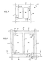
- a partially diagrammatic and partially schematic diagram of one embodiment of the pixel 88 is illustrated.
- the common electrode 54 is not illustrated, but would substantially overlie the areas of the electrode segments 60 and 62.
- Separate y line connections 64 are shown as well as separate x line connections 66 to the pixel electrode segments 60 and 62. Electrically these are equivalent to the schematic diagram in Fig. 3.
- Each of the lines 84, 86, 94 and 96 is isolated from one another.
- the pixel 88 is illustrated in top plan view in Fig. 8 and a side sectional view in Fig. 9.
- the cross sectional view in Fig. 9 is taken along the line 9-9', 9'-9" and 9"-9"' in Fig. 8.
- the pixel 88 is formed on an insulative substrate 98, such as glass.
- the electrode segments 60 and 62 are formed on the substrate 98 and can be formed of a transparent conductive layer 100, such as deposited indium tin oxide (ITO).
- ITO deposited indium tin oxide
- the lines or leads 86 and 96 are also formed on the substrate 98.
- the lines 86 and 96 can be formed from the ITO layer 100 and a top metal layer 102, or they can be formed from just a conductive material such as metal, for example, aluminum, molybdenum, or a molybdenum tantalum alloy. Other suitable metals are chromium, tantalum tungsten, palladium and platinum.
- the lines 86 and 96 can be formed by, for example, magnetron sputtering the metal over the entire surface area of the glass substrate 98 and then removing selected portions of the deposited metal by utilizing a mask and photolithography techniques of the types well known in the art.
- the isolation devices 80, 82, 90 and 92 then are formed, preferably from a deposited semiconductor material. Tne devices are formed as diodes for illustration purposes, but can be any of the above enumerated isolation devices.
- the deposited semiconductor material is preferably an amorphous semiconductor alloy including silicon.
- the amorphous silicon alloy can also include hydrogen and/or fluorine and can be deposited by plasma assisted chemical vapor deposition i.e. glow discharge as disclosed, for example, in U.S. Patent No. 4,226,898 which issued on October 7, 1980 in the names of Stanford R. Ovshinsky and Arun Madan for Amorphous Semiconductors Equivalent To Crystalline Semiconductors Produced By A Glow Discharge Process.
- the diodes preferably have a p-i-n configuration, best illustrated in Fig. 9, formed by a first doped region 80a and 92a, which can be n-type, an intrinsic region 80b and 92b overlying the first doped regions 80a and 92a respectively, and a second doped region 80c and 92c, which can be p-type, overlying the intrinsic regions 80b and 92b respectively.
- the diodes also preferably include a top conductive layer 80d and 92d.
- the diodes can be formed by depositing the previously mentioned conductive layer 100, metal layer 102, amorphous silicon alloy regions and top conductive layer over the entire surface area of the substrate 98, and thereafter selectively etching portions of the top ' metal layer and amorphous silicon alloy regions by utilizing a suitable mask and conventional photolithography techniques.
- the mask utilized during the etching process preferably defines a diode configuration wherein each diode is about 20 to 50 microns on a side.
- Representative thicknesses for the amorphous silicon alloy regions can be, for example, 300 to 1,000 Angstroms and preferably 500 Angstroms for the p-type regions, 1,000 to 10,000 Angstroms and preferably 3,000 Angstroms for the intrinsic regions, and 100 to 500 Angstroms and preferably 200 Angstroms for the n-type regions.
- the diode patterned resist is removed and new resist layers are coated and patterned to form the electrode segments 60 and 62 without the metal layer 102 and the bottom lines 86 and 96 with the metal layer 102.
- the bottom lines 86 and 96 can first be formed of metal and then the diodes formed thereon.
- the diode 80 is formed on the electrode segment 60, the diode 90 on the electrode segment 62, the diode 92 on the line 96 and the diode 82 on the line 86.
- a layer of insulating material 104 is next formed over the lines 86 and 96, the substrate 98, the electrode segments 60 and 62, and the diodes 80, 82, 90 and 92.
- the insulating material 104 can be formed from any deposited insulator such as silicon oxide (Si x O y )) or silicon nitride (Si x Ny), for example.
- the insulating layer 104 is patterned to define openings or vias 106, 108, 110 and 112 which communicate with the diodes 80, 82, 90 and 92.
- the layer 104 is also patterned to expose the electrode segments 60 and 62.
- the pattern of the layer 104 can be obtained by depositing the insulator, for example, over the entire surface area, coating a layer of photoresist over the insulator layer, and then exposing and developing out both of the photoresist and the insulator using a further mask. This step forms the openings or vias 106, 108, 110 and 112 and uncovers upper surface portions of the electrode segments 60 and 62.
- the top lines 64, 66, 84 and 94 are then formed coupling the lines, diodes and electrode segments together.
- the top lines can be formed of a conductive material of the same type as described for the lines 86 and 96.
- the conductive material for the top lines is generally chosen to be different than that of the bottom lines to obtain a differential etch.
- a top passivation layer 114 is then formed over the exposed surfaces, which layer is patterned to expose the electrode segments 60 and 62.
- the top passivation layer 114 can be formed of the same materials and in the same manner as the layer 104.
- Tnis forms a completed subassembly of the display and pixel 88.
- the subassembly is an intermediate product in the manufacturing of the display.
- the subassembly can be stocked for later use or sold for completion into a display by anotner party. Further, as more fully described in copending application, Case No. 753, entitled “High Yield Liquid Crystal Display And Method Of Making Same", filed concurrently herewith, the subassembly can be electronically tested prior to adding the light influencing material since the electronic circuitry is all on the one substrate 98.
- Fig. 10 illustrates a cross sectional side view of the pixel 88 along the line 9-9 of Fig. 8 with a top plane 116, the common electrode 54 and the pixel liquid crystal display material 58.
- the pixel 88 in Fig. 10 is a completed display pixel.
- Figs. 8-10 is not drawn to scale and that the common electrode 54 and the electrode segments 60 and 62 define the light influencing display area of the pixel 54.
- the electrodes are substantially coextensive and can be configured in a square configuration as illustrated in Fig. 8 and can be, for example, 300 to 2,000 microns on a side depending on the overall size of the finished display matrix and the desired aspect ratio.
- the light influencing material 58 can be of any conventional variety, as for example nematic liquid crystal display material.
- the diodes of the displays can be formed from deposited semiconductor materials other than amorphous semiconductor alloys which need not be deposited materials.
- the diodes can be formed from polycrystalline semiconductor alloys.
- the diodes can be formed in a stacked or tandem configuration.
- the isolation devices can be other than diodes, such as transistors or other dual polarity devices.
- the electrodes could be further subdivided.
- the pixel common electrode could be divided into two electrode segments and the segmented electrode could be divided into three spaced apart electrode segments with the address lines coupled only to the two outer segmented electrode segments.
Landscapes
- Physics & Mathematics (AREA)
- Nonlinear Science (AREA)
- Mathematical Physics (AREA)
- Chemical & Material Sciences (AREA)
- Crystallography & Structural Chemistry (AREA)
- General Physics & Mathematics (AREA)
- Optics & Photonics (AREA)
- Engineering & Computer Science (AREA)
- Microelectronics & Electronic Packaging (AREA)
- Geometry (AREA)
- Liquid Crystal (AREA)
- Devices For Indicating Variable Information By Combining Individual Elements (AREA)
Priority Applications (1)
| Application Number | Priority Date | Filing Date | Title |
|---|---|---|---|
| AT85106404T ATE101285T1 (de) | 1984-06-29 | 1985-05-24 | Anzeigevorrichtungen und unteranordnungen mit pixelelektroden. |
Applications Claiming Priority (2)
| Application Number | Priority Date | Filing Date | Title |
|---|---|---|---|
| US06/626,133 US4589733A (en) | 1984-06-29 | 1984-06-29 | Displays and subassemblies having improved pixel electrodes |
| US626133 | 1984-06-29 |
Publications (3)
| Publication Number | Publication Date |
|---|---|
| EP0166948A2 true EP0166948A2 (fr) | 1986-01-08 |
| EP0166948A3 EP0166948A3 (en) | 1988-05-25 |
| EP0166948B1 EP0166948B1 (fr) | 1994-02-02 |
Family
ID=24509081
Family Applications (1)
| Application Number | Title | Priority Date | Filing Date |
|---|---|---|---|
| EP85106404A Expired - Lifetime EP0166948B1 (fr) | 1984-06-29 | 1985-05-24 | Dispositifs d'affichage et sous-ensembles avec électrodes pour les éléments d'image |
Country Status (6)
| Country | Link |
|---|---|
| US (1) | US4589733A (fr) |
| EP (1) | EP0166948B1 (fr) |
| JP (1) | JPS6156384A (fr) |
| AT (1) | ATE101285T1 (fr) |
| CA (1) | CA1242783A (fr) |
| DE (1) | DE3587740T2 (fr) |
Cited By (4)
| Publication number | Priority date | Publication date | Assignee | Title |
|---|---|---|---|---|
| FR2604014A1 (fr) * | 1985-03-04 | 1988-03-18 | Gen Electric | Dispositif de conversion de l'information comportant des lignes auxiliaires d'adresses afin d'ameliorer le rendement de fabrication |
| EP0263589A3 (en) * | 1986-10-09 | 1989-06-07 | Ovonic Imaging Systems, Inc. | Liquid crystal display having pixels with auxiliary capacitance |
| WO1994019720A1 (fr) * | 1993-02-26 | 1994-09-01 | Honeywell Inc. | Affichage a cristaux liquides a demi-teinte autoreferences |
| EP1679560A2 (fr) * | 2004-11-25 | 2006-07-12 | Océ-Technologies B.V. | Elément de formation d'image pour le dispositif d'impression avec un circuit multiplex pour contrôler les électrodes à former d'images |
Families Citing this family (28)
| Publication number | Priority date | Publication date | Assignee | Title |
|---|---|---|---|---|
| US5061040A (en) * | 1984-01-23 | 1991-10-29 | Ois Optical Imaging Systems, Inc. | Liquid crystal displays operated by amorphous silicon alloy diodes |
| US4728172A (en) * | 1984-08-08 | 1988-03-01 | Energy Conversion Devices, Inc. | Subassemblies for displays having pixels with two portions and capacitors |
| US4917474A (en) * | 1984-09-10 | 1990-04-17 | Semiconductor Energy Laboratory Co., Ltd. | Optoelectronic panel and method of making the same |
| JPS6188578A (ja) * | 1984-10-08 | 1986-05-06 | Nec Corp | 非線形素子 |
| EP0184341B1 (fr) * | 1984-11-12 | 1994-01-26 | Semiconductor Energy Laboratory Co., Ltd. | Ecran d'affichage à cristal liquide et sa méthode de fabrication |
| JPS61117521A (ja) * | 1984-11-12 | 1986-06-04 | Semiconductor Energy Lab Co Ltd | 半導体装置作製方法 |
| US4715685A (en) * | 1985-03-04 | 1987-12-29 | Energy Conversion Devices, Inc. | Liquid crystal display having potential source in a diode ring |
| JPS61217087A (ja) * | 1985-03-22 | 1986-09-26 | 富士電機株式会社 | 液晶表示装置用非線形抵抗素子 |
| JPH0617957B2 (ja) * | 1985-05-15 | 1994-03-09 | セイコー電子工業株式会社 | 液晶表示装置 |
| GB8604402D0 (en) * | 1986-02-21 | 1986-03-26 | Gen Electric Co Plc | Liquid crystal displays |
| US5042917A (en) * | 1986-04-25 | 1991-08-27 | Matsushita Electric Industrial Co., Ltd. | Liquid crystal matrix display unit |
| NL8601373A (nl) * | 1986-05-29 | 1987-12-16 | Philips Nv | Weergeefinrichting met verbeterde aansturing. |
| US4782340A (en) * | 1986-08-22 | 1988-11-01 | Energy Conversion Devices, Inc. | Electronic arrays having thin film line drivers |
| JP2816549B2 (ja) * | 1986-10-22 | 1998-10-27 | セイコーインスツルメンツ株式会社 | 電気光学装置 |
| JPS63186216A (ja) * | 1987-01-28 | 1988-08-01 | Nec Corp | アクテイブマトリツクス液晶表示器 |
| JPS63281134A (ja) * | 1987-05-13 | 1988-11-17 | Fuji Electric Co Ltd | アクティブマトリックス形表示パネル |
| JPS64929A (en) * | 1987-06-23 | 1989-01-05 | Toyota Motor Corp | Liquid crystal display element |
| FR2632435B1 (fr) * | 1988-06-01 | 1991-02-15 | Maurice Francois | Ecran d'affichage permettant de visualiser le contour d'une image et procede de commande d'un tel ecran |
| JPH02137366A (ja) * | 1988-11-18 | 1990-05-25 | Nec Corp | ダイオード型アクティブマトリクス基板 |
| US5122889A (en) * | 1988-12-22 | 1992-06-16 | Nec Corporation | Active matrix liquid crystal display using mim diodes having symmetrical voltage-current characteristics as switching elements |
| JP2600929B2 (ja) * | 1989-01-27 | 1997-04-16 | 松下電器産業株式会社 | 液晶画像表示装置およびその製造方法 |
| US5179035A (en) * | 1989-09-15 | 1993-01-12 | U.S. Philips Corporation | Method of fabricating two-terminal non-linear devices |
| US5456860A (en) * | 1990-03-31 | 1995-10-10 | Merck Patent Gesellschaft Mit Beschrankter Haftung | Matrix liquid-crystal display |
| JPH07175087A (ja) * | 1993-12-20 | 1995-07-14 | Nec Corp | 液晶表示装置 |
| KR20000004422A (ko) | 1998-06-30 | 2000-01-25 | 김영환 | 고개구율 액정표시소자의 화소전극 형성방법 |
| KR20070006834A (ko) * | 2004-04-13 | 2007-01-11 | 코닌클리케 필립스 일렉트로닉스 엔.브이. | 액정 표시 장치 |
| US7832093B2 (en) * | 2007-06-11 | 2010-11-16 | Kent State University | Method of creating an electro-mechanical energy conversion device |
| EP4200832A4 (fr) * | 2020-08-19 | 2024-07-17 | OLEDWorks LLC | Circuit de pixel pour la réduction de la diaphonie |
Family Cites Families (18)
| Publication number | Priority date | Publication date | Assignee | Title |
|---|---|---|---|---|
| US3073992A (en) * | 1959-11-19 | 1963-01-15 | Westinghouse Electric Corp | Display device |
| US3603984A (en) * | 1969-09-24 | 1971-09-07 | Rca Corp | Panel structure for matrix addressed displays |
| US3654606A (en) * | 1969-11-06 | 1972-04-04 | Rca Corp | Alternating voltage excitation of liquid crystal display matrix |
| US3630015A (en) * | 1970-01-20 | 1971-12-28 | Kurt Lehovec | Light transformation device |
| JPS5526447B2 (fr) * | 1972-06-05 | 1980-07-14 | ||
| US4008564A (en) * | 1972-06-09 | 1977-02-22 | Luce Nunzio A | Liquid crystal display device |
| US3834794A (en) * | 1973-06-28 | 1974-09-10 | Beckman Instruments Inc | Liquid crystal electric field sensing measurement and display device |
| US4062626A (en) * | 1974-09-20 | 1977-12-13 | Hitachi, Ltd. | Liquid crystal display device |
| US4226898A (en) * | 1978-03-16 | 1980-10-07 | Energy Conversion Devices, Inc. | Amorphous semiconductors equivalent to crystalline semiconductors produced by a glow discharge process |
| US4170772A (en) * | 1978-04-26 | 1979-10-09 | The United States Of America As Represented By The Secretary Of The Army | Flat panel display with full color capability |
| US4163677A (en) * | 1978-04-28 | 1979-08-07 | Rca Corporation | Schottky barrier amorphous silicon solar cell with thin doped region adjacent metal Schottky barrier |
| US4223308A (en) * | 1979-07-25 | 1980-09-16 | Northern Telecom Limited | LCDs (Liquid crystal displays) controlled by thin film diode switches |
| US4431271A (en) * | 1979-09-06 | 1984-02-14 | Canon Kabushiki Kaisha | Display device with a thin film transistor and storage condenser |
| JPS57500848A (fr) * | 1980-06-27 | 1982-05-13 | ||
| JPS5849912A (ja) * | 1981-08-25 | 1983-03-24 | Kyocera Corp | 液晶光シヤツタ− |
| US4642620A (en) * | 1982-09-27 | 1987-02-10 | Citizen Watch Company Limited | Matrix display device |
| JPS5978388A (ja) * | 1982-10-28 | 1984-05-07 | 三洋電機株式会社 | 液晶表示パネルの表示電極構造 |
| US4537471A (en) * | 1983-12-23 | 1985-08-27 | Hughes Aircraft Company | Liquid crystal pixel driver circuit and matrix display |
-
1984
- 1984-06-29 US US06/626,133 patent/US4589733A/en not_active Expired - Fee Related
-
1985
- 1985-05-24 AT AT85106404T patent/ATE101285T1/de active
- 1985-05-24 DE DE85106404T patent/DE3587740T2/de not_active Expired - Fee Related
- 1985-05-24 EP EP85106404A patent/EP0166948B1/fr not_active Expired - Lifetime
- 1985-06-06 CA CA000483344A patent/CA1242783A/fr not_active Expired
- 1985-06-28 JP JP60142400A patent/JPS6156384A/ja active Pending
Cited By (4)
| Publication number | Priority date | Publication date | Assignee | Title |
|---|---|---|---|---|
| FR2604014A1 (fr) * | 1985-03-04 | 1988-03-18 | Gen Electric | Dispositif de conversion de l'information comportant des lignes auxiliaires d'adresses afin d'ameliorer le rendement de fabrication |
| EP0263589A3 (en) * | 1986-10-09 | 1989-06-07 | Ovonic Imaging Systems, Inc. | Liquid crystal display having pixels with auxiliary capacitance |
| WO1994019720A1 (fr) * | 1993-02-26 | 1994-09-01 | Honeywell Inc. | Affichage a cristaux liquides a demi-teinte autoreferences |
| EP1679560A2 (fr) * | 2004-11-25 | 2006-07-12 | Océ-Technologies B.V. | Elément de formation d'image pour le dispositif d'impression avec un circuit multiplex pour contrôler les électrodes à former d'images |
Also Published As
| Publication number | Publication date |
|---|---|
| DE3587740T2 (de) | 1994-05-05 |
| US4589733A (en) | 1986-05-20 |
| EP0166948A3 (en) | 1988-05-25 |
| EP0166948B1 (fr) | 1994-02-02 |
| JPS6156384A (ja) | 1986-03-22 |
| CA1242783A (fr) | 1988-10-04 |
| ATE101285T1 (de) | 1994-02-15 |
| DE3587740D1 (de) | 1994-03-17 |
Similar Documents
| Publication | Publication Date | Title |
|---|---|---|
| US4589733A (en) | Displays and subassemblies having improved pixel electrodes | |
| US4728172A (en) | Subassemblies for displays having pixels with two portions and capacitors | |
| US4639087A (en) | Displays having pixels with two portions and capacitors | |
| US4728175A (en) | Liquid crystal display having pixels with auxiliary capacitance | |
| EP0193759B1 (fr) | Affichage à matrice active sans croisement des lignes d'adressage sur les substrats et procédé pour le commander | |
| US4653864A (en) | Liquid crystal matrix display having improved spacers and method of making same | |
| EP0460747B1 (fr) | Procédé de fabrication de matrices de dispositifs du type MIM et dispositifs d'affichages comportant de telles matrices | |
| EP0329887B1 (fr) | Dispositif d'affichage à cristaux liquides | |
| US5231039A (en) | Method of fabricating a liquid crystal display device | |
| EP0842455A4 (fr) | Transistors a film mince ameliores, leur procede de fabrication et affichages matriciels les contenant | |
| US4820024A (en) | Active matrix display | |
| RU2066074C1 (ru) | Активная отображающая матрица для жидкокристаллических экранов | |
| US4944575A (en) | Electrooptical display screen and a method of fabrication of said screen | |
| US5508765A (en) | Matrix-addressed type display device | |
| US4929569A (en) | Method of fabricating amorphous silican diode addressed liquid crystal display | |
| US5061040A (en) | Liquid crystal displays operated by amorphous silicon alloy diodes | |
| JPS61153692A (ja) | 光影響性デイスプレイで使用されるプログラム可能な半導体スイツチ及びその製法 | |
| US5295008A (en) | Color LCD panel | |
| EP0150728A2 (fr) | Dispositifs d'affichage à cristal liquide commandés par des diodes comprenant des alliages amorphes de silicium | |
| JPH04133035A (ja) | 光弁基板用単結晶薄膜半導体装置 | |
| EP0150798B1 (fr) | Dispositifs d'affichage à cristal liquide commandés par des diodes comprenant des alliages amorphes de silicium | |
| US4738513A (en) | Liquid crystal display including a non-linear resistance element | |
| US5689153A (en) | Electro-optical plasma display device with electrode having insulating layers | |
| JP2668317B2 (ja) | アクティブマトリクスパネル | |
| EP0335724A2 (fr) | Riseau de transistor couche mince pour un dispositif électro-optique et procédé pour sa fabrication |
Legal Events
| Date | Code | Title | Description |
|---|---|---|---|
| PUAI | Public reference made under article 153(3) epc to a published international application that has entered the european phase |
Free format text: ORIGINAL CODE: 0009012 |
|
| AK | Designated contracting states |
Designated state(s): AT BE CH DE FR GB IT LI LU NL SE |
|
| PUAL | Search report despatched |
Free format text: ORIGINAL CODE: 0009013 |
|
| AK | Designated contracting states |
Kind code of ref document: A3 Designated state(s): AT BE CH DE FR GB IT LI LU NL SE |
|
| 17P | Request for examination filed |
Effective date: 19881115 |
|
| 17Q | First examination report despatched |
Effective date: 19910405 |
|
| RAP1 | Party data changed (applicant data changed or rights of an application transferred) |
Owner name: OIS OPTICAL IMAGING SYSTEMS, INC. |
|
| GRAA | (expected) grant |
Free format text: ORIGINAL CODE: 0009210 |
|
| AK | Designated contracting states |
Kind code of ref document: B1 Designated state(s): AT BE CH DE FR GB IT LI LU NL SE |
|
| ITF | It: translation for a ep patent filed | ||
| REF | Corresponds to: |
Ref document number: 101285 Country of ref document: AT Date of ref document: 19940215 Kind code of ref document: T |
|
| REF | Corresponds to: |
Ref document number: 3587740 Country of ref document: DE Date of ref document: 19940317 |
|
| ET | Fr: translation filed | ||
| EPTA | Lu: last paid annual fee | ||
| PLBE | No opposition filed within time limit |
Free format text: ORIGINAL CODE: 0009261 |
|
| STAA | Information on the status of an ep patent application or granted ep patent |
Free format text: STATUS: NO OPPOSITION FILED WITHIN TIME LIMIT |
|
| 26N | No opposition filed | ||
| EAL | Se: european patent in force in sweden |
Ref document number: 85106404.8 |
|
| PGFP | Annual fee paid to national office [announced via postgrant information from national office to epo] |
Ref country code: SE Payment date: 19960531 Year of fee payment: 12 Ref country code: NL Payment date: 19960531 Year of fee payment: 12 Ref country code: GB Payment date: 19960531 Year of fee payment: 12 Ref country code: FR Payment date: 19960531 Year of fee payment: 12 Ref country code: AT Payment date: 19960531 Year of fee payment: 12 |
|
| PGFP | Annual fee paid to national office [announced via postgrant information from national office to epo] |
Ref country code: LU Payment date: 19960601 Year of fee payment: 12 |
|
| PGFP | Annual fee paid to national office [announced via postgrant information from national office to epo] |
Ref country code: CH Payment date: 19960603 Year of fee payment: 12 |
|
| PGFP | Annual fee paid to national office [announced via postgrant information from national office to epo] |
Ref country code: DE Payment date: 19960621 Year of fee payment: 12 |
|
| PGFP | Annual fee paid to national office [announced via postgrant information from national office to epo] |
Ref country code: BE Payment date: 19960711 Year of fee payment: 12 |
|
| PG25 | Lapsed in a contracting state [announced via postgrant information from national office to epo] |
Ref country code: LU Free format text: LAPSE BECAUSE OF NON-PAYMENT OF DUE FEES Effective date: 19970524 Ref country code: GB Effective date: 19970524 Ref country code: AT Effective date: 19970524 |
|
| PG25 | Lapsed in a contracting state [announced via postgrant information from national office to epo] |
Ref country code: SE Effective date: 19970525 |
|
| PG25 | Lapsed in a contracting state [announced via postgrant information from national office to epo] |
Ref country code: LI Free format text: LAPSE BECAUSE OF NON-PAYMENT OF DUE FEES Effective date: 19970531 Ref country code: CH Free format text: LAPSE BECAUSE OF NON-PAYMENT OF DUE FEES Effective date: 19970531 Ref country code: BE Effective date: 19970531 |
|
| BERE | Be: lapsed |
Owner name: OPTICAL IMAGING SYSTEMS INC. OIS Effective date: 19970531 |
|
| PG25 | Lapsed in a contracting state [announced via postgrant information from national office to epo] |
Ref country code: NL Effective date: 19971201 |
|
| GBPC | Gb: european patent ceased through non-payment of renewal fee |
Effective date: 19970524 |
|
| REG | Reference to a national code |
Ref country code: CH Ref legal event code: PL |
|
| PG25 | Lapsed in a contracting state [announced via postgrant information from national office to epo] |
Ref country code: FR Free format text: LAPSE BECAUSE OF NON-PAYMENT OF DUE FEES Effective date: 19980130 |
|
| EUG | Se: european patent has lapsed |
Ref document number: 85106404.8 |
|
| NLV4 | Nl: lapsed or anulled due to non-payment of the annual fee |
Effective date: 19971201 |
|
| PG25 | Lapsed in a contracting state [announced via postgrant information from national office to epo] |
Ref country code: DE Free format text: LAPSE BECAUSE OF NON-PAYMENT OF DUE FEES Effective date: 19980203 |
|
| REG | Reference to a national code |
Ref country code: FR Ref legal event code: ST |