EP0184341B1 - Ecran d'affichage à cristal liquide et sa méthode de fabrication - Google Patents
Ecran d'affichage à cristal liquide et sa méthode de fabrication Download PDFInfo
- Publication number
- EP0184341B1 EP0184341B1 EP85308217A EP85308217A EP0184341B1 EP 0184341 B1 EP0184341 B1 EP 0184341B1 EP 85308217 A EP85308217 A EP 85308217A EP 85308217 A EP85308217 A EP 85308217A EP 0184341 B1 EP0184341 B1 EP 0184341B1
- Authority
- EP
- European Patent Office
- Prior art keywords
- layer
- substrate
- laminate
- liquid crystal
- conductive layer
- Prior art date
- Legal status (The legal status is an assumption and is not a legal conclusion. Google has not performed a legal analysis and makes no representation as to the accuracy of the status listed.)
- Expired - Lifetime
Links
Images








Classifications
-
- G—PHYSICS
- G02—OPTICS
- G02F—OPTICAL DEVICES OR ARRANGEMENTS FOR THE CONTROL OF LIGHT BY MODIFICATION OF THE OPTICAL PROPERTIES OF THE MEDIA OF THE ELEMENTS INVOLVED THEREIN; NON-LINEAR OPTICS; FREQUENCY-CHANGING OF LIGHT; OPTICAL LOGIC ELEMENTS; OPTICAL ANALOGUE/DIGITAL CONVERTERS
- G02F1/00—Devices or arrangements for the control of the intensity, colour, phase, polarisation or direction of light arriving from an independent light source, e.g. switching, gating or modulating; Non-linear optics
- G02F1/01—Devices or arrangements for the control of the intensity, colour, phase, polarisation or direction of light arriving from an independent light source, e.g. switching, gating or modulating; Non-linear optics for the control of the intensity, phase, polarisation or colour
- G02F1/13—Devices or arrangements for the control of the intensity, colour, phase, polarisation or direction of light arriving from an independent light source, e.g. switching, gating or modulating; Non-linear optics for the control of the intensity, phase, polarisation or colour based on liquid crystals, e.g. single liquid crystal display cells
-
- G—PHYSICS
- G02—OPTICS
- G02F—OPTICAL DEVICES OR ARRANGEMENTS FOR THE CONTROL OF LIGHT BY MODIFICATION OF THE OPTICAL PROPERTIES OF THE MEDIA OF THE ELEMENTS INVOLVED THEREIN; NON-LINEAR OPTICS; FREQUENCY-CHANGING OF LIGHT; OPTICAL LOGIC ELEMENTS; OPTICAL ANALOGUE/DIGITAL CONVERTERS
- G02F1/00—Devices or arrangements for the control of the intensity, colour, phase, polarisation or direction of light arriving from an independent light source, e.g. switching, gating or modulating; Non-linear optics
- G02F1/01—Devices or arrangements for the control of the intensity, colour, phase, polarisation or direction of light arriving from an independent light source, e.g. switching, gating or modulating; Non-linear optics for the control of the intensity, phase, polarisation or colour
- G02F1/13—Devices or arrangements for the control of the intensity, colour, phase, polarisation or direction of light arriving from an independent light source, e.g. switching, gating or modulating; Non-linear optics for the control of the intensity, phase, polarisation or colour based on liquid crystals, e.g. single liquid crystal display cells
- G02F1/133—Constructional arrangements; Operation of liquid crystal cells; Circuit arrangements
- G02F1/136—Liquid crystal cells structurally associated with a semi-conducting layer or substrate, e.g. cells forming part of an integrated circuit
- G02F1/1362—Active matrix addressed cells
- G02F1/1365—Active matrix addressed cells in which the switching element is a two-electrode device
Definitions
- the present invention relates to a liquid crystal display panel which employs liquid crystal pixel elements each of which has a nonlinear element having a diode characteristic and a liquid crystal element.
- the invention also pertains to methods for the manufacture of the liquid crystal display panel.
- the liquid crystal pixel element M ij is connected to a row conductive layer F i and a column conductive layer H j at their intersection.
- an image display can be provided by driving the liquid crystal pixel elements M11 to M mn using the row conductive layers F i to F m and the column conductive layers H1 to H n .
- the conventional type of display panel is complex in the structure of the non linear element U ij , in the structure of the liquid crystal element L ij and in the structure for connecting the liquid crystal pixel element M ij to the row conductive layer F i and the column conductive layer H j .
- Another object of the present invention is to provide novel methods for the manufacture of such a liquid crystal display panel.
- the second substrate member including a second substrate and a plurality of n x q, where q is an integer equal to or greater than 1, stripe-like conductive layers H11, H12 ... H 1q ; H21 ... H22 ... H 2q ; ... and H n1 , H n2 ...
- each non-linear element U ij is a laminate A ij of a first layer Q ij arranged on a portion D ij of the respective row electrode F i , each layer Q ij being arranged in the row direction and having substantially the same width w as the row electrode F i , and a second conductive layer E i formed on the layer Q ij and having substantially the same width w as the layer Q ij , the two side faces of the laminate A ij extending in the row direction being covered with insulating material (K ij , K ij '; K i ), and the respective display electrode C ij has substantially the same width as the length of the laminate and extends in a column direction over the laminate A ij and onto the
- the liquid crystal display panel comprises (a) first and second substrate members disposed opposite at a predetermined distance in substantially parallel relation to each other and (b) liquid crystal filled between the first and second substrate members.
- the second substrate member comprises (a) a second substrate having an insulating surface, and (b) a plurality n x q (where q is an integer equal to or greater than 1) of stripe-like conductive layers H11, H12 ... H 1q ; H21, H22 ... H 2q ; ... and H n1 , H n2 H n3 ... H nq sequentially arranged on the second substrate in the row direction and extending in the column direction, the conductive layers H j1 to H jq being opposite the conductive layers C 1j to C mj .
- the laminate member A ij forms a nonlinear element U ij .
- the liquid crystal element L ijr can be driven by applying a driving signal to the liquid crystal display element M ijr via the row conductive layer F i and the column conductive layer H jr . Accordingly, the liquid crystal display panel provides an image display.
- the liquid crystal element L ijr is formed by the conductive layer H jr , the portion B ijr of the conductive layer C ij facing the conductive layer H jr and the portion of the liquid crystal between the conductive layer H jr and the portion B ijr , as mentioned above, the liquid crystal element L ijr is simple in structure.
- the nonlinear element U ij is formed by the aforementioned laminate member A ij , and hence is simple in construction.
- the liquid crystal display panel of the present invention is simple-structured in that the liquid crystal display element L ijr and the nonlinear element U ij are interconnected in series via the conductive layer C ij to constitute the liquid crystal display device M ijr and in that the liquid crystal display device M ijr is connected at one side to the row conductive layer F i forming the other electrode of the nonlinear element U ij and at the other side to the column conductive layer H jr forming the other electrode of the liquid display element L ijr .
- the liquid crystal display panel of the present invention is far simpler in structure than is conventional, in consequence of which m x (m x q) display crystal elements M111 to M mnq can be arranged in an m x (n x q) matrix form with a high density, ensuring to provide an image display with high resolution.
- the liquid crystal display panel which has the aforesaid excellent feature can be produced by a manufacturing method of the present invention which includes a step of (A) preparing a first substrate member, (B) preparing a second substrate member, (C) turning the second substrate member upside down and disposing the first and second substrate members in opposing and substantially parallel relation to each other and (D) filling liquid crystal in the gap defined by the first and second substrate members.
- the step of preparing a second substrate member includes the steps of forming, on a second substrate having an insulating surface, a plurality of n x q, where q is an integer equal to or greater than 1, conductive layers H11, H12 ... H 1q ; H21, H22 ... H 2q ; ... and H n1 , H n2 ... H nq sequentially arranged in the row direction and extending in the column direction, the conductive layers H j1 , H j2 , ... and H iq corresponding to the display electrodes C 1j , C 2j , ... and C mj of the first substrate member.
- the manufacturing method of the present invention requires only three masks for the fabrication of the liquid crystal display, that is, one for the formation of the laminate member A1 to A m , one for the formation of the conductive layers C11 to C mn and the laminate members A11 to A mn and one for the formation of the conductive layers H11 ⁇ H 1r to H n1 ⁇ H nr .
- liquid crystal display panel having the aforesaid advantages can easily be manufactured at low cost.
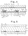
- Figs. 1 to 5 illustrate an embodiment of the liquid crystal display panel of the present invention, in which a substrate 1 has an insulating surface.
- the substrate 1 is formed of, for instance, alkaline free glass.
- the substrate 1 has sequentially arranged thereon in column direction a plurality m of row conductive layers F1, F2 ... F m .
- the row conductive layer F i also called row electrode, may preferable be composed of a layer 2 formed of, for example, aluminum and a nontransparent layer 3 formed of, for instance chromium.
- the row conductive layer F i has sequentially formed thereon a plurarity of n layers Q i1 , Q i2 ... Q in each of which is formed, for example, non-single-crystal semiconductor.
- the layers Q i1 , Q i2 ... Q in have same width as the row conductive layer F i .
- the layer Q ij also may be only a very thin insulating layer which may pass tunnel current. But Figs. 1 to 5 show the case where the layer Q ij has the n-i-n type structure. For the sake of brevity, the following description will be made in connection with the case where the layer Q ij has the n-i-n type structure.
- the layer Q ij has an n-type non-single-crystal silicon layer 21 formed on the row conductive layer F i , an i-type layer 22 of non-single-crystal semconductor formed on the layer 21 and an n-type non-single-crystal silicon layer 23 formed on the layer 22.
- the layer 22 is formed principally of silicon but contains carbon (C), nitrogen (N) or oxygen (O) in an amount of 1/10 or less relative to the silicon, and hence is formed of non-single-crystal semiconductor expressed by Si x C 1-x (where 0 ⁇ x ⁇ 1).
- the layer Q ij is covered over the entire area of its top surface with a conductive layer E ij .
- the conductive layer E ij is formed of, for instance, chromium.
- the part of the conductive layer F i underlying the layer Q ij , the layer Q ij and the conductive layer E ij make up a layer member A ij .
- the layer member A ij are covered over the entire area of its opposite side surfaces with insulating layers K ij and K ij ', respectively.
- the insulating layers K ij and K ij ' are formed of, for instance, silicon nitride or silicon oxide and have 0.1 to 0.5 ⁇ m in thickness.
- the substrate 1 has arranged thereon in a matrix form m x n (where m > 1, and n > 1) conductive layers C11 to C 1n , C21 to C 2n , C31 to C 3n , ... and C m1 to C mn , these layers C ij being also called display electrodes.
- the conductive layer C ij extends on the layer member A ij i.e. the conductive layer E ij and the insulating layer K ij and K ij ' through the side surface of the insulating layer K ij and make contact with the conductive layer E ij .
- the conductive layer C ij has substantially same width as the long of the layer member A ij i.e. the conductive layer E ij and is formed of, for instance, chromium and is nontransparent.
- the opposing side surfaces of the conductive layer C ij which determine the width of the conductive layer C ij are substantially aligned with the opposing side surfaces of the layer member A ij , which determine the long of the layer member A ij .
- a relatively thin insulation protecting layer 25 is deposited on the substrate 1 to cover the conductive layer C11 to C mn , the active layers A11 to A 1n , A21 to A 2n ... A m1 to A mn , the insulating layer K11 to K mn and K11' to K mn ' and parts of the row conductive layers F1, F2 ... F m which are not covered with the conductive layers C11 to C 1n , C21 to C2...C m1 to C mn .
- the conductive layers F1 to F m , the layer members A11 to A mn , the insulating layers K11 to K mn and K11' to K mn ' and the conductive layers C11 to C mn make up a substrate member 7.
- the substrate member 7 is formed, for example, as follows: A conductive layer F which will ultimately form the row conductive layers F1 to F m , a layer Q which will ultimately form the layers Q11 to Q mn and a conductive layer E which will ultimately form the conductive layers E11 to E mn are deposited in that order on the substrate 1, as shown in Figs. 9A to 9E.
- the conductive layer F, the layer Q and the conductive layer E make up a layer member A which will ultimately form the layer members A11 to A mn .
- the conductive layer F may be formed by a known method, for instance, a sputtering or electron beam evaporation process.
- the layer Q also may be formed by a known method, for example, a CVD, plasma CVD or photo CVD method.
- the substrate 1 formed thereon the conductive layer F was loaded through a loading and unloading chamber into a first reaction chamber, wherein a glow discharge was produced over the substrate 1 at a high frequency of 13.56 MHz in an atmosphere containing silane SiH4, phosphine PH3 and hydrogen, with the substrate temperature held in the range of 200 to 250 °C.
- an n-type microcrystalline silicon layer which had a conductivity of 10 ⁇ 2 to 102 ( ⁇ cm) ⁇ 1 and contained hydrogen as a recombination center neutralizer, was deposited 300 to 1000 ⁇ thick on the conductive layer F.
- the substrate 1 was returned from the second reaction chamber to the first reaction chamber, wherein another n-type layer similar to the above n-type layer was deposited by the same method on the i-type non-single-crystal silicon layer, thus obtaining the laminate member Q having the n-i-n type structure.
- the conductive layer E may also be formed by a known method, for instance, a sputtering or electron beam evaporation process.
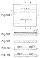
- the layer member A is subjected to a known pattern process using a first mask, providing m layer members A1 to A m of the same pattern as row the conductive layers F1 to F m , as shown in Figs. 10A to 10E.
- a insulating layer K which will ultimately form the insulating layer K11 to K mn and K11' to K mn ' and which is relatively thin than the layer member A1 to A m is deposited by a known method, for example, plasma CVD method on the entire surface of the substrate 1 to cover the active layers A1 to A m , as shown in Figs. 11A to 11E.
- the insulating layer K is selectively etched away by a known method, for example, a plasma etching method to form insulating layers K i and K i ' on both sides of the laminate member A i difining the width of the laminate member A i , as shown in Fisg. 12A to 12E.
- a plasma etching method to form insulating layers K i and K i ' on both sides of the laminate member A i difining the width of the laminate member A i , as shown in Fisg. 12A to 12E.
- a conductive layer C is diposited on the entire area of the substrate 1 to cover the laminate member A1 to A m and the insulating layers K1 to K m and K1' to K m ' as shown in Figs. 13A to 13E.
- the conductive layer C, the layer Q1 to Q m and the conductive layer E1 to E m of the layer members A1 to A m are patterned by a known method using a second mask into the conductive layers C11 to C mn , the layers Q11 to Q mn and the conductive layers E11 to E mn as shown in Figs. 14A to 14E.
- the conductive layer F1 to F m are not patterned.
- the layer Q ij , the part of the conductive layer F i underlying the layer Q ij and the conductive layer E ij make up the laminate member A ij .
- the insulating layers K1 to K m and K1' to K m ' are selectively etched away by a known mthod into the insulating layer K11 to K mn and K11' to K mn '.
- the thin insulation protecting layer 25 is deposited on the entire surface of the substrate 1 to cover the conductive layers C11 to C mn , the layer members A11 to A mn , the insulating layers K11 to K mn and K11' to K mn ' and the part of the conductive layer F1 to F m which are not covered with the conductive layers C11 to C nm .
- the column conductive layer H j1 , H j2 and H j3 can be obtained by forming a conductive layer through a known method on the substrate 12 and then patterning the conductive layer through a third mask.
- the column conductive layers H j1 , H j2 and H j3 are covered over entire surfaces thereof with red, green and blue filters S j1 , S j2 and S j3 , respectively.
- a insulation protecting layer 26 formed of, for instance, organic region is deposited on the entire surface of the substrate 12 by a known method, for example, coating to cover the filters S11 to S n1 , S12 to S n2 and S13 to S n3 .
- the substrate member 11 is disposed upside down by a suitable support means (not shown) in opposing relation to the top of the substrate member 7 in parallel thereto.
- a suitable support means not shown
- the conductive layers C 1j to C mj of the substrate member 7 and the column conductive layers H j1 , H j2 and H j3 of the substrate member 11 are held face-to face with each other.
- a space defined by the substrate members 7 and 11 is filled with liquid crystal 13.
- the layer member A ij constitute a nonlinear element U ij which employs the part 17 of the conductive layer F i underlying the layer Q ij and the conductive layer E ij as its electrodes D ij and D ij ', respectively.
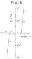
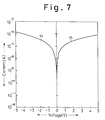
- the element U ij presents such a nonlinear voltage(V)-current(A) characteristic curves 51 and 61 as shown in Figs. 6 and 7.
- the element U ij has an offset voltage which is intermediate between the voltage that makes the liquid crystal element L ijr transparent and non transparent, respectively.
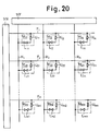
- the liquid crystal element L ijr and the nonlinear element U ij are connected in series with each other, and hence make up a liquid crystal display device M ijr .
- the electrode B ijr of the liquid crystal element L ijr and the electrode D ijr ' of the nonlinear element U ij are common each other.
- the electrode B ijr ' of the liquid crystal elements L 1jr of the liquid crystal display devices M ijr is connected to the column conductive layer H jr and the electrode D ij of the nonlinear element U ij is connected to the conductive layer F i .
- the column conductive layer H j1 , H j2 and H j3 are covered with the red, green and blue filters S j1 , S j2 and S j3 , respectively.
- liquid crystal element L ijr can be controlled to be transparent or nontransparent, respectively, by applying, through use of row and column decoders 51X and 51Y, across the liquid crystal display device M ij1 , M ij2 and M ij3 via the conductive layers F1 and H j1 , F i and H j2 , and F i and H j3 red, as shown in Fig. 8, green and blue drive signals a color display can be provided.
- the liquid crystal display panel shown in Figs. 1 to 5 can be provided a color image display.
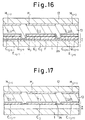
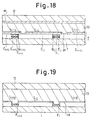
- Fig. 15 to 19 illustrate another embodiment of the liquid crystal display panel of the present invention.
- the liquid crystal display panel shown in Figs. 15 to 19 has the same construction as depicted in Figs. 1 to 5 except the following points:
- the insulating layers K i1 to K in and K (i+1)1 ' to K (i+1)n ' in Figs. 1 to 5 are substituted with a insulating layer K i .
- the insulating layer K i extends between the laminate members A i1 to A in and A (i+1)1 to A (i+1)n and substantially flush therewith, therefor the conductive layer C ij is formed on the ensulating layer K i and extends onto the laminate member A ij and the insulating layer K (i-1) .
- the column conductive layer H i1 , H j2 and H j3 in Figs. 1 to 5 are substituted with a column conductive layer H j , and therefor the liquid crystal display device M ij1 , M ij2 and M ij3 are substituted with a liquid crystal display device M ij .
- the filters S11 to S n1 , s12 to S n2 and S13 to S n3 are omitted.
- the electrode B ijr of the liquid crystal element L ij and the electrode D ij ' of the nonlinear element U ij are common each other.
- the electrode V ij ' of the liquid crystal elements L 1j of the liquid crystal display devices M ij is connected to the column conductive layer H j and the electrode D ij of the nonlinear element U ij is connected to the conductive layer F i . Therefore, according to the arrangement described above in connection with Figs.
- liquid crystal element L ij can be controlled to be transparent or nontransparent, respectively, by applying, through use of row and column decoders 51X and 51Y, across the liquid crystal display device M ij , M ij and M ij via the conductive layers F i and H j drive signal a monocolor display can be provided.
- the liquid crystal display panel shown in Figs. 1 to 5 can be provided a monocolor image display.
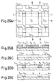
- the substrate member 7 dipicted in Figs. 15 to 19 can be manufactured, for example, as follows:
- a conductive layer F which will ultimately form the conductive layers F1 to F n , a layer laminate member which will ultimately form the layer laminate members Q11 to Q mn and a conductive layer E, which will ultimately form the conductive layers E11 to E mn are deposited in that order on the substrate 1, as shown in Figs. 21A to 21E as in the case with the example shown Figs. 9A to 9E.
- the conductive layer F, the non-single-crystal semiconductor layer Q and the conductive layer E make up a active layer member A which will ultimately form the active layer member A11 to A mn as described previously.
- the active layer member A is subjected to a known pattern process using a first mask, providing m layer members A1 to A m of the same pattern as the conductive layers F1 to F m , as shown in Figs. 22A to 22E, as is the case with the example shown in Figs. 10A to 10E.
- a insulating layer K of photo resist which will ultimately form the insulating layer K i is deposited by a known method, for example, a plasma CVD method on the entire surface of the substrate 1 to cover the layers A1 to A m , as shown in Figs. 23A to 23E.
- the insulating layer K is irradiated by light 30 without using any mask as shown in Figs. 23A to 23B and then is developed into the insulating layer K i , as shown in Figs. 25A to 24E.
- a conductive layer C is diposited on the entire area of the substrate 1 to cover the laminate member A1 to A m and the insulating layer K1 to K m as shown in Figs. 25A to 25E.
- the conductive layer C, the conductive layers E1 to E m and the layers Q1 to Q m of the layer member A1 to A m are patterned by a known method using a second mask into the conductive layers C11 to C mn , the layers Q11 to Q mn and the conductive layers E11 to E mn of the layer member A11 to A mn , as shown in Figs. 26A to 26E.
- the thin insulating layer 25 is deposited on the entire surface of the substrate 1 to cover the conductive layers C11 to C mn , the layer members A11 to A mn , the insulating layers K1 to K m and the parts of the conductive layers F1 to F m which are not covered with the conductive layers C11 to C mn .
Landscapes
- Physics & Mathematics (AREA)
- Nonlinear Science (AREA)
- Chemical & Material Sciences (AREA)
- Crystallography & Structural Chemistry (AREA)
- General Physics & Mathematics (AREA)
- Optics & Photonics (AREA)
- Engineering & Computer Science (AREA)
- Microelectronics & Electronic Packaging (AREA)
- Mathematical Physics (AREA)
- Liquid Crystal (AREA)
- Devices For Indicating Variable Information By Combining Individual Elements (AREA)
Claims (6)
- Affichage d'éléments d'image (pixels) à cristaux liquides comportant: un premier et un deuxième élément formant substrat (7, 11) placés en opposition à une distance prédéterminée, essentiellement en parallèle l'un par rapport à l'autre, et un cristal liquide (13) remplissant l'espace entre les premier et deuxième éléments formant substrat;
le premier élément formant substrat (7) comprenant un premier substrat (1), m électrodes de ligne semblables à des raies F₁, F₂... Fm, agencées sur la surface intérieure dudit premier substrat, chaque électrode de ligne ayant une largeur w, et n électrodes d'affichage Cij, où j = 1, 2...n, couplées à chaque électrode de ligne Fi, où i = 1, 2...m, à travers un élément Uij respectif non linéaire, ayant une caractéristique de diode;
le deuxième élément formant substrat (11), comprenant un deuxième substrat (12) et un groupe de n x q, où q est un nombre entier égal ou supérieur à 1, couches conductrices semblables à des raies H₁₁, H₁₂, H1q; H₂₁ ... H₂₂ ... H2q; ... et Hn1, Hn2 ... Hnq, agencées d'une manière séquentielle sur la surface intérieure dudit deuxième substrat (12) dans la direction de ligne et s'étendant dans la direction de colonne, les couches conductrices Hj1 à Hjq étant opposées aux électrodes d'affichage C1j à Cmj;
caractérisé en ce que chaque élément Uij non linéaire est un revêtement laminé Aij d'une première couche Qij, agencée sur une partie Dij de l'électrode Fi de ligne respective, chaque couche Qij étant agencée dans la direction de ligne et ayant essentiellement la même largeur w que l'électrode Fi de ligne, et d'une seconde couche Ei conductrice formée sur la couche Qij et ayant essentiellement la même largeur w que la couche Qij, les deux faces latérales du revêtement laminé Aij s'étendant dans la direction de ligne, étant recouvertes d'un matériau isolant (Kij, Kij'; Ki), et l'électrode Cij d'affichage respective a essentiellement la même largeur que la longueur du revêtement laminé et s'étend dans la direction de colonne sur le revêtement laminé Aij et sur le matériau isolant. - Affichage selon la revendication 1, dans lequel le matériau isolant Ki formé sur le substrat s'étend entre les éléments formant revêtement laminé Ai1 à Ain, situés côte à côte et est essentiellement à leur niveau.
- Affichage selon la revendication 1, dans lequel le matériau isolant Kij, Kij' ne recouvre essentiellement que les faces latérales du revêtement laminé Aij.
- Procédé de fabrication d'un panneau d'affichage à cristaux liquides comportant:(A) une étape de préparation d'un premier élément formant substrat qui comprend les étapes de:(a) formation, sur un premier substrat, d'un élément formant revêtement laminé A composé d'une couche conductrice F, d'une couche Q et d'une couche conductrice E laminées dans cet ordre;(b) modelage de l'élément formant revêtement laminé A dans un premier groupe de m éléments formant revêtement laminé A₁ à Am analogues à des raies, agencés d'une manière séquentielle dans la direction de colonne et s'étendant dans la direction de ligne;(c) dépôt d'une couche K isolante sur toute la surface du premier substrat pour recouvrir les éléments formant revêtement laminé A₁ à Am;(d) attaque sélective de la couche isolante K pour former des couches isolantes Ki (et Ki') des deux côtés de l'élément formant revêtement laminé Ai (où i = 1, 2... m) définissant la largeur des éléments formant revêtement laminé Ai;(e) formation d'une couche conductrice C sur toute la surface du premier substrat pour recouvrir les éléments formant revêtement laminé A₁ à Am et les couches isolantes K₁ à Km (et K₁' à Km'); et(f) modelage de la couche conductrice C, des deuxièmes couches conductrices E₁ à Em et des couches Q₁ à Qm pour former des électrodes d'affichage Ci1 à Cin s'étendant sur l'élément formant revêtement laminé Ai et sur la couche isolante Ki et pour former à partir de chaque élément formant revêtement laminé Ai, un groupe de n éléments formant revêtement laminé séparés Aij (pour j = 1 à n), chacun étant composé d'une couche conductrice Eij, d'une couche Qij et d'une partie Dij de l'électrode de ligne Fi sous-jacente à la couche Qij(B) une étape de préparation d'un deuxième élément formant substrat, qui comprend les étapes de:
formation, sur un deuxième substrat ayant une surface isolante, d'un groupe de n x q, où q est un nombre entier égal ou supérieur à 1, couches conductrices H₁₁, H₁₂, ... H1q; H₂₁, H₂₂ ... H2q; ... et Hn1, Hn2 ... Hnq agencées d'une manière séquentielle dans la direction de ligne et s'étendant dans la direction de colonne, les couches conductrices Hj1, HJ2, ... et Hiq correspondant aux électrodes d'affichage C1j , C2j , ... et Cmj du premier élément formant substrat;(C) une étape pour renverser de haut en bas le deuxième élément formant substrat et pour placer les premier et deuxième éléments formant substrat en opposition et essentiellement en parallèle l'un par rapport à l'autre et(D) une étape de remplissage du cristal liquide dans l'espace défini par les premier et deuxième éléments formant substrat. - Procédé selon la revendication 4, dans lequel l'étape (d) comporte l'attaque de la couche K isolante laissant des parties de ladite couche isolante ne s'étendre essentiellement que le long des surfaces latérales des éléments formant revêtement laminé et non pas le long du substrat, et dans lequel l'étape (f) comprend le modelage de la couche conductrice C pour former des électrodes d'affichage Ci1 à Cin s'étendant du substrat sur la couche isolante Ki et sur l'élément formant revêtement laminé Ai et passant sur la face latérale de la couche isolante Ki.
- Procédé selon la revendication 4, dans lequel l'étape (d) comporte l'attaque de la couche K isolante pour former une couche isolante Ki s'étendant entre les éléments formant revêtement laminé A₁ à Am situés côte à côte et étant essentiellement à leur niveau.
Applications Claiming Priority (4)
| Application Number | Priority Date | Filing Date | Title |
|---|---|---|---|
| JP238986/84 | 1984-11-12 | ||
| JP59238986A JPS61117522A (ja) | 1984-11-12 | 1984-11-12 | 表示装置 |
| JP59277414A JPS61151615A (ja) | 1984-12-26 | 1984-12-26 | 半導体装置 |
| JP277414/84 | 1984-12-26 |
Publications (3)
| Publication Number | Publication Date |
|---|---|
| EP0184341A2 EP0184341A2 (fr) | 1986-06-11 |
| EP0184341A3 EP0184341A3 (en) | 1988-04-20 |
| EP0184341B1 true EP0184341B1 (fr) | 1994-01-26 |
Family
ID=26534017
Family Applications (1)
| Application Number | Title | Priority Date | Filing Date |
|---|---|---|---|
| EP85308217A Expired - Lifetime EP0184341B1 (fr) | 1984-11-12 | 1985-11-12 | Ecran d'affichage à cristal liquide et sa méthode de fabrication |
Country Status (5)
| Country | Link |
|---|---|
| US (3) | US4828363A (fr) |
| EP (1) | EP0184341B1 (fr) |
| KR (2) | KR900006938B1 (fr) |
| CN (1) | CN1003959B (fr) |
| DE (1) | DE3587737T2 (fr) |
Families Citing this family (8)
| Publication number | Priority date | Publication date | Assignee | Title |
|---|---|---|---|---|
| JPS62112128A (ja) * | 1985-11-11 | 1987-05-23 | Semiconductor Energy Lab Co Ltd | 液晶装置 |
| GB2203881B (en) * | 1987-04-16 | 1991-03-27 | Philips Electronic Associated | Liquid crystal display device |
| JP2534311B2 (ja) * | 1988-04-04 | 1996-09-11 | 出光興産株式会社 | 液晶光学素子の製造方法 |
| US5220316A (en) * | 1989-07-03 | 1993-06-15 | Benjamin Kazan | Nonlinear resistor control circuit and use in liquid crystal displays |
| GB2236424A (en) * | 1989-09-15 | 1991-04-03 | Philips Electronic Associated | Active matrix display device and their fabrication |
| JPH07294725A (ja) * | 1994-03-01 | 1995-11-10 | Seiko Instr Inc | カラーフィルター及び多色液晶表示装置の製造方法 |
| US6849935B2 (en) | 2002-05-10 | 2005-02-01 | Sarnoff Corporation | Low-cost circuit board materials and processes for area array electrical interconnections over a large area between a device and the circuit board |
| USRE41914E1 (en) | 2002-05-10 | 2010-11-09 | Ponnusamy Palanisamy | Thermal management in electronic displays |
Family Cites Families (17)
| Publication number | Priority date | Publication date | Assignee | Title |
|---|---|---|---|---|
| US3654606A (en) * | 1969-11-06 | 1972-04-04 | Rca Corp | Alternating voltage excitation of liquid crystal display matrix |
| US3912366A (en) * | 1973-12-06 | 1975-10-14 | Ibm | Liquid crystal display assembly having polyimide layers |
| US4413883A (en) * | 1979-05-31 | 1983-11-08 | Northern Telecom Limited | Displays controlled by MIM switches of small capacitance |
| US4223308A (en) * | 1979-07-25 | 1980-09-16 | Northern Telecom Limited | LCDs (Liquid crystal displays) controlled by thin film diode switches |
| US4448491A (en) * | 1979-08-08 | 1984-05-15 | Canon Kabushiki Kaisha | Image display apparatus |
| GB2081018B (en) * | 1980-07-31 | 1985-06-26 | Suwa Seikosha Kk | Active matrix assembly for display device |
| US4472027A (en) * | 1980-12-25 | 1984-09-18 | Canon Kabushiki Kaisha | Method for the orientation of liquid crystal and liquid crystal display device |
| NL8103376A (nl) * | 1981-07-16 | 1983-02-16 | Philips Nv | Weergeefinrichting. |
| JPS59137930A (ja) * | 1983-01-28 | 1984-08-08 | Fuji Photo Film Co Ltd | カラ−光プリンタヘツド |
| EP0126914A2 (fr) * | 1983-04-12 | 1984-12-05 | Granotechnik AG | Unité de contrôle pour un dispositif d'affichage sensible aux champs électriques au moyen d'éléments semi-conducteurs |
| US4561726A (en) * | 1983-07-29 | 1985-12-31 | At&T Bell Laboratories | Alignment of ferroelectric LCDs |
| JPS6047471A (ja) * | 1983-08-26 | 1985-03-14 | Fuji Electric Corp Res & Dev Ltd | 半導体放射線検出器 |
| IL70116A (en) * | 1983-11-02 | 1987-02-27 | Stolov Michael | Liquid crystal device for displaying multicolor images |
| JPS60218627A (ja) * | 1984-04-13 | 1985-11-01 | Sharp Corp | カラ−液晶表示装置 |
| US4589733A (en) * | 1984-06-29 | 1986-05-20 | Energy Conversion Devices, Inc. | Displays and subassemblies having improved pixel electrodes |
| US4666252A (en) * | 1984-06-29 | 1987-05-19 | Energy Conversion Devices, Inc. | High yield liquid crystal display and method of making same |
| US4639087A (en) * | 1984-08-08 | 1987-01-27 | Energy Conversion Devices, Inc. | Displays having pixels with two portions and capacitors |
-
1985
- 1985-11-12 EP EP85308217A patent/EP0184341B1/fr not_active Expired - Lifetime
- 1985-11-12 KR KR1019850008495A patent/KR900006938B1/ko not_active Expired
- 1985-11-12 DE DE85308217T patent/DE3587737T2/de not_active Expired - Fee Related
- 1985-11-12 KR KR1019850008495A patent/KR860004326A/ko active Granted
- 1985-11-12 CN CN85109301.9A patent/CN1003959B/zh not_active Expired
-
1987
- 1987-09-03 US US07/092,594 patent/US4828363A/en not_active Expired - Lifetime
- 1987-09-03 US US07/092,532 patent/US4846558A/en not_active Expired - Lifetime
- 1987-12-28 US US07/140,939 patent/US4850679A/en not_active Expired - Lifetime
Also Published As
| Publication number | Publication date |
|---|---|
| EP0184341A2 (fr) | 1986-06-11 |
| DE3587737D1 (de) | 1994-03-10 |
| KR860004326A (ko) | 1986-06-20 |
| CN1003959B (zh) | 1989-04-19 |
| US4828363A (en) | 1989-05-09 |
| DE3587737T2 (de) | 1994-05-05 |
| CN85109301A (zh) | 1986-10-22 |
| US4846558A (en) | 1989-07-11 |
| US4850679A (en) | 1989-07-25 |
| EP0184341A3 (en) | 1988-04-20 |
| KR900006938B1 (ko) | 1990-09-25 |
Similar Documents
| Publication | Publication Date | Title |
|---|---|---|
| US4917474A (en) | Optoelectronic panel and method of making the same | |
| EP0166948B1 (fr) | Dispositifs d'affichage et sous-ensembles avec électrodes pour les éléments d'image | |
| US5453134A (en) | Solar cell | |
| US7247227B2 (en) | Buffer layer in flat panel display | |
| US4728172A (en) | Subassemblies for displays having pixels with two portions and capacitors | |
| US4730903A (en) | Ferroelectric crystal display panel and manufacturing method thereof | |
| US5008590A (en) | Display arrangement having pin diode switching elements | |
| EP0184341B1 (fr) | Ecran d'affichage à cristal liquide et sa méthode de fabrication | |
| US4820024A (en) | Active matrix display | |
| US5039620A (en) | Method of making a photoelectric conversion device with a high response speed | |
| US4744862A (en) | Manufacturing methods for nonlinear semiconductor element and liquid crystal display panel using the same | |
| US6107736A (en) | Organic electroluminescent display device and method of fabrication | |
| US4844588A (en) | Liquid crystal display panel and manufacturing method thereof | |
| EP0229397B1 (fr) | Dispositif de conversion photo-électrique et méthode pour sa fabrication | |
| US4929569A (en) | Method of fabricating amorphous silican diode addressed liquid crystal display | |
| CN222750822U (zh) | 显示面板及显示装置 | |
| US5061040A (en) | Liquid crystal displays operated by amorphous silicon alloy diodes | |
| JPS60191291A (ja) | 非晶質シリコン合金ダイオ−ドにより作動される液晶デイスプレイ | |
| EP0178190B1 (fr) | Ecran optoélectronique et sa méthode de fabrication | |
| JPH0746721B2 (ja) | イメ−ジセンサおよびその製造方法 | |
| EP0150798B1 (fr) | Dispositifs d'affichage à cristal liquide commandés par des diodes comprenant des alliages amorphes de silicium | |
| JPS61151614A (ja) | 半導体装置作製方法 | |
| JPH067598B2 (ja) | 太陽電池の製造方法 | |
| JPS61151615A (ja) | 半導体装置 | |
| CN121240722A (zh) | 显示面板及其制作方法、显示装置 |
Legal Events
| Date | Code | Title | Description |
|---|---|---|---|
| PUAI | Public reference made under article 153(3) epc to a published international application that has entered the european phase |
Free format text: ORIGINAL CODE: 0009012 |
|
| AK | Designated contracting states |
Kind code of ref document: A2 Designated state(s): DE FR GB |
|
| 17P | Request for examination filed |
Effective date: 19860430 |
|
| RBV | Designated contracting states (corrected) |
Designated state(s): DE FR GB |
|
| PUAL | Search report despatched |
Free format text: ORIGINAL CODE: 0009013 |
|
| AK | Designated contracting states |
Kind code of ref document: A3 Designated state(s): DE FR GB |
|
| 17Q | First examination report despatched |
Effective date: 19910408 |
|
| GRAA | (expected) grant |
Free format text: ORIGINAL CODE: 0009210 |
|
| AK | Designated contracting states |
Kind code of ref document: B1 Designated state(s): DE FR GB |
|
| REF | Corresponds to: |
Ref document number: 3587737 Country of ref document: DE Date of ref document: 19940310 |
|
| ET | Fr: translation filed | ||
| PLBE | No opposition filed within time limit |
Free format text: ORIGINAL CODE: 0009261 |
|
| STAA | Information on the status of an ep patent application or granted ep patent |
Free format text: STATUS: NO OPPOSITION FILED WITHIN TIME LIMIT |
|
| 26N | No opposition filed | ||
| PGFP | Annual fee paid to national office [announced via postgrant information from national office to epo] |
Ref country code: GB Payment date: 19961104 Year of fee payment: 12 |
|
| PGFP | Annual fee paid to national office [announced via postgrant information from national office to epo] |
Ref country code: FR Payment date: 19961111 Year of fee payment: 12 |
|
| PGFP | Annual fee paid to national office [announced via postgrant information from national office to epo] |
Ref country code: DE Payment date: 19961115 Year of fee payment: 12 |
|
| PG25 | Lapsed in a contracting state [announced via postgrant information from national office to epo] |
Ref country code: GB Free format text: LAPSE BECAUSE OF NON-PAYMENT OF DUE FEES Effective date: 19971112 |
|
| PG25 | Lapsed in a contracting state [announced via postgrant information from national office to epo] |
Ref country code: FR Free format text: THE PATENT HAS BEEN ANNULLED BY A DECISION OF A NATIONAL AUTHORITY Effective date: 19971130 |
|
| GBPC | Gb: european patent ceased through non-payment of renewal fee |
Effective date: 19971112 |
|
| PG25 | Lapsed in a contracting state [announced via postgrant information from national office to epo] |
Ref country code: DE Free format text: LAPSE BECAUSE OF NON-PAYMENT OF DUE FEES Effective date: 19980801 |
|
| REG | Reference to a national code |
Ref country code: FR Ref legal event code: ST |