EP0167076A2 - Digitale Schaltung mit MESFETs - Google Patents
Digitale Schaltung mit MESFETs Download PDFInfo
- Publication number
- EP0167076A2 EP0167076A2 EP85107745A EP85107745A EP0167076A2 EP 0167076 A2 EP0167076 A2 EP 0167076A2 EP 85107745 A EP85107745 A EP 85107745A EP 85107745 A EP85107745 A EP 85107745A EP 0167076 A2 EP0167076 A2 EP 0167076A2
- Authority
- EP
- European Patent Office
- Prior art keywords
- mesfet
- electrically connected
- directly electrically
- electrode
- source
- Prior art date
- Legal status (The legal status is an assumption and is not a legal conclusion. Google has not performed a legal analysis and makes no representation as to the accuracy of the status listed.)
- Granted
Links
Images
Classifications
-
- H—ELECTRICITY
- H03—ELECTRONIC CIRCUITRY
- H03K—PULSE TECHNIQUE
- H03K19/00—Logic circuits, i.e. having at least two inputs acting on one output; Inverting circuits
- H03K19/0008—Arrangements for reducing power consumption
- H03K19/0016—Arrangements for reducing power consumption by using a control or a clock signal, e.g. in order to apply power supply
-
- H—ELECTRICITY
- H03—ELECTRONIC CIRCUITRY
- H03K—PULSE TECHNIQUE
- H03K19/00—Logic circuits, i.e. having at least two inputs acting on one output; Inverting circuits
- H03K19/02—Logic circuits, i.e. having at least two inputs acting on one output; Inverting circuits using specified components
- H03K19/08—Logic circuits, i.e. having at least two inputs acting on one output; Inverting circuits using specified components using semiconductor devices
- H03K19/094—Logic circuits, i.e. having at least two inputs acting on one output; Inverting circuits using specified components using semiconductor devices using field-effect transistors
- H03K19/0952—Logic circuits, i.e. having at least two inputs acting on one output; Inverting circuits using specified components using semiconductor devices using field-effect transistors using Schottky type FET MESFET
Definitions
- This invention relates to digital circuits including metal-semiconductor field-effect transistors (MESFET).
- MOSFETS metal-oxide semiconductor FETS
- inverter see transistor 16, Figure 1 therein.
- enhancement mode MOSFETS serve to separately invert logic signals and separately drive two enhancement mode MOSFETS in complementary fashion.
- US-A 4 380 709 depletion mode MOSFETS are driven in complementary fashion by separate inverters, each of the inverters employing a depletion mode MOSFET.
- circuits disclosed in these patents each include means for placing the circuits in a third or standby state.
- a disable signal is provided by using two depletion mode MOSFETS. When the circuit is disabled, the output pin is left floating and a high impedance will be present at the logic output pin.
- US-A 4 363 978 a "float" mode exists in which the output circuit will neither supply current to the output load or switch the output load to ground, and therefore other drivers can control the logic state of the output load.
- This patent provides float and non-float signals through separate enhancement mode MOSFETS.
- a disable circuit employs four MOSFETS (including depletion and enhancement types) and leaves the output floating when activated.
- MESFETS offer advantages over MOSFET circuits. This is particularly true when the substrate is GaAs instead of silicon due to the high mobility of electrons in GaAs.
- the invention discloses an integrated circuit having a substrate, wherein the source of a first MESFET is directly electrically connected to the drain of a second MESFET and both MESFETS are driven in complementary fashion by logic signals controlled by an inverter which includes a third MESFET.
- the combination is connected between a voltage supply and ground.
- the third MESFET has its drain directly electrically connected to an electrical load (which in turn is connected to a second voltage supply) and its source connected to ground.
- the third MESFET serves as an inverter with the logic input being applied to its gate and the logic output being taken from its drain.
- the drain of the third MESFET is connected to the gate of the first MESFET.
- the logic signal input to the gate of the third MESFET is also directly input to the gate of the second MESFET.
- the logic output of the entire circuit is taken at the connection between the source of the first MESFET and the drain of the second MESFET.
- the logic input signal applied to the gates of the second and third MESFETS will drive the first and second MESFETS in complementary fashion.
- a further improvement of the invention includes means for selectively disconnecting the electrical load from the second voltage supply. This provides a third or standby state of the circuit where the output floats and the circuit is at high impedance.
- depletion mode MESFETS are employed as the first, second and third MESFETS and GaAs is the substrate material. If depletion mode MESFETS are used, the output from the third MESFET/inverter, will be level shifted to accommodate the negative threshold voltages of the depletion mode MESFETS. Further improvements and details are described in the subclaims. The invention will now be described with reference to the attached drawings, in which
- MESFET refers to the commonly recognized structure of a metallic gate (or gates) overlying a solid substrate between ohmic source and drain.contacts.
- the substrate is selected to provide a flow of majority carriers between the source and drain contacts upon the application of a sufficient potential difference between the contacts. The flow of majority carriers is controlled by the potential difference between the gate and the substrate.
- Doped regions of a first conductivity type are provided beneath each of the source and drain contacts.
- the channel region beneath the metallic gate is a doped region of either a first or second conductivity type.
- the channel region is doped with the first conductivity type, providing a negative bias voltage on the gate relative to the source produces a depletion mode device, and providing a positive biasing voltage on the gate relative to the source produces an enhancement mode device. If the channel region is doped with the second conductivity type and the second conductivity type is P-type, a positive gate to source potential difference produces an enhancement device, whereas if the second conductivity type is N-type a negative gate to source potential difference produces an enhancement device.
- Circuit 10 of Figure 1 includes first 12, second 14 and third 16 MESFETS, an electrical load 18, an input 20, a logic output 22, and a voltage reference point (e.g., ground).
- the drain of MESFET 12 is directly electrically connected to a first voltage supply (v DDl ), and the source of MESFET 12 is directly electrically connected to the drain of MESFET 16 and logic output node 22.
- the source of MESFET 16 is directly electrically connected to ground.
- the drain of MESFET 14 is directly electrically connected to electrical load 18, which in turn is directly electrically connected to a second voltage supply (V DD2 ).
- the source of MESFET 14 is directly electrically connected to ground.
- the drain of MESFET 14 is also electrically connected to the gate of MESFET 12, either directly or through a voltage level shifter 24 connected between the drain of MESFET 14 and the gate of MESFET 12.
- Input 20 is directly electrically connected to the gates of MESFETS 14 and 16.
- the first and second voltage supplies may be the same supply depending on one's desires and design considerations, but the supplies are shown separately to depict the most general case. If MESFETS 10, 14 and 16 are depletion mode MESFETS, voltage level shifter 24 is generally employed to reduce "low" logic voltage values at the drain of MESFET 14 to below the threshold voltage of ME SFE T 12. This insures that MESFET 12 will be off when the drain voltage of MESFET 14 is low.
- circuit 10 receives either a high or low logic voltage signal at input 20. If the logic voltage signal applied to input 20 is high, MESFETS 14 and 16 will be turned on. The drain of MESFET 14 will be pulled near to ground, i.e., a low logic value. The low voltage at the drain of MESFET 14 will (after being shifted by voltage level shifter 24) turn MESFE T 12 off. With MESFET 12 off and MESFET 16 on, logic output node 22 is pulled towards ground thereby producing a low logic output value at node 22 and for circuit 10.
- MESFETS 14 and 16 will be turned off.
- the voltage at the drain of MESFET 14 will be pulled towards V DD2 , i.e., a high logic value.
- the high value at the drain of MESFET 14 will in turn (and after being shifted by voltage level shifter 24) turn MESFET 12 on.
- logic output node 22 is pulled towards V DD1 thereby producing a high logic output value at node 22 and for circuit 10.
- MESFET 14 and load 18 serve as an inverter which is employed to drive MESFETS 12 and 16 in complementary fashion.
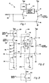
- Circuit 10 is expanded in circuit 26 of Figure 2. Corresponding components in circuits 10 and 26 are like numbered for clarity.
- circuit 26 employs voltage level shifting means 24 as the first of two voltage level shifting means and separates voltage level shifting means 24 into a first resistance means 24a and a first current source 24b.
- Circuit 26 further includes ME SFET 28, disabling means 29 (disabling means 29 is preferably MESFET 30), a second resistance means 32 and a second current source 34.
- Resistance means 32 and current source 34 comprise a second voltage level shifting means 35.
- First voltage level shifting means 24 has an input 36 and output 38
- second voltage level shifting means 35 has an input 40 and output 42.
- Load 18 has a first terminating region (i.e., the same node as input 36) and a second terminating region 44.
- Circuit 26 also includes a logic input 46 which is directly electrically connected to the gate of MESFET 28 and an enable input 48 which is directly electrically connected to the gate of MESFET 30.
- the drain of MESFET 30 is directly electrically connected to V DD2 , and the source of MESFET 30 is directly electrically connected to the drain of MESFET 28.
- the source of MESFET 28 is directly electrically connected to input 40 of the second voltage level shifting means 35.
- the output 42 of the second voltage level shifting means is directly electrically connected to current source 34 and to input node 20.
- the first terminating region 36 of the first voltage level shifting means 24 is directly electrically connected to the drain of MESFET 14.
- the second terminating region 38 of the first voltage level shifting means 24 is directly electrically connected to current source 24b and to the gate of MESFET 12.
- disable means 29 is preferably MESFET 30.
- MESFET 30 is a depletion mode MESFET
- load 18 is a depletion mode MESFET 50 with source and gate shorted.
- current sources 24b and 34 are MESFETS 52 and 54, respectively, with their sources and gates shorted and the source of each of MESFETS 52 and 54 is directly electrically connected to a third voltage supply V SS which is negative relative to ground.
- V SS negative relative to ground.
- circuits 10 and 26 function in the same manner. It should be noted that the current source 24b is selected so that diode 56 is always forward biased. Similarly, current source 34 keeps the series of diodes 58, 60 and 62 always forward biased.
- disable means 29 disconnects circuit 26 from voltage supply V DD2 (i.e., MESFET 30 is off).
- MESFET 30 When MESFET 30 is off, circuit 26 is placed in a third standby mode. In the standby mode, logic output node 22 floats and circuit impedance is very high. Logic signals applied to input 46 will not affect node 22 when the enable signal is low.
- the standby mode is a particularly valuable feature which allows circuit 26 to consume as little as one tenth of the power consumed as when circuit 26 is enabled.
- disable means 29 connects V DD2 to the drain of MESFET 28 and to load 18.
- logic signals applied to input 46 are either high or low. If the logic signal applied at input 46 is high, MESFET 28 is turned on pulling the source of MESFET 28 high which in turn (as described above for circuit 10) results in MESFET 16 being turned on and MESFET 12 being turned off. Logic output node 22 goes low in this case.
- MESFET 28 If the logic signal applied at input 46 is low when circuit 26 is in the enabled mode, MESFET 28 is turned off dropping the drain of MESFET 28 low. This in turn (after the low voltage at the drain of MESFET 28 is further appropriately reduced by second voltage level shifting means 35) results in MESFET 16 being turned off and MESFET 12 being turned on pulling logic output node 22 high.
- diodes 56, 58, 60 and 62 are all the same. This means that the voltage levels of the outputs from the source of MESFET 28 and the drain of M ESFET 14 are shifted by different amounts. This difference is needed in circuit 26 because the threshold voltages of MESFETS 12 and 16 are different due to the extra voltage drop to ground which MESFET 12 experiences (as compared to MESFET 16) as a result of leakage through MESFET 16 when MESFET 16 is off.
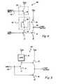
- Figure 3 depicts an alternative disabling means 29 wherein an enhancement mode MESFET is employed instead of a depletion mode MESFET as MESFET 30.
- the alternative of Figure 3 could be used in circuit 26 or in the enhancement mode version of circuit 26 (i.e., circuit 64) shown in Figure 4. Note that corresponding components of circuits 26 and 64 are numbered the same.
- Circuit 64 employs only one depletion mode MESFE T (i.e., 50), and does not require MESFETS 28 and 54 or diodes 58, 60 and 62, which served to shift the logic input voltage level in circuit 26.
- circuit 66 An enhancement mode MESFET version of circuit 10 is shown as circuit 66 in Figure 5. Again corresponding components of circuits 10 and 66 are like numbered. Note that in circuit 64 and 66 the voltage level shifting means are deleted because the output voltages need not be compensated for negative threshold voltages when enhancements mode MESFETS are being switched.
Landscapes
- Engineering & Computer Science (AREA)
- Physics & Mathematics (AREA)
- Computer Hardware Design (AREA)
- Computing Systems (AREA)
- General Engineering & Computer Science (AREA)
- Mathematical Physics (AREA)
- Power Engineering (AREA)
- Logic Circuits (AREA)
Applications Claiming Priority (2)
| Application Number | Priority Date | Filing Date | Title |
|---|---|---|---|
| US06/625,151 US4631426A (en) | 1984-06-27 | 1984-06-27 | Digital circuit using MESFETS |
| US625151 | 1984-06-27 |
Publications (3)
| Publication Number | Publication Date |
|---|---|
| EP0167076A2 true EP0167076A2 (de) | 1986-01-08 |
| EP0167076A3 EP0167076A3 (en) | 1987-10-07 |
| EP0167076B1 EP0167076B1 (de) | 1992-03-11 |
Family
ID=24504815
Family Applications (1)
| Application Number | Title | Priority Date | Filing Date |
|---|---|---|---|
| EP85107745A Expired EP0167076B1 (de) | 1984-06-27 | 1985-06-22 | Digitale Schaltung mit MESFETs |
Country Status (5)
| Country | Link |
|---|---|
| US (1) | US4631426A (de) |
| EP (1) | EP0167076B1 (de) |
| JP (1) | JPH069337B2 (de) |
| CA (1) | CA1246157A (de) |
| DE (1) | DE3585564D1 (de) |
Cited By (5)
| Publication number | Priority date | Publication date | Assignee | Title |
|---|---|---|---|---|
| FR2599910A1 (fr) * | 1986-06-10 | 1987-12-11 | Labo Electronique Physique | Circuit amplificateur differentiel regenerateur de signaux complementaires de faible amplitude |
| GB2207319A (en) * | 1987-05-19 | 1989-01-25 | Gazelle Microcircuits Inc | Compound semiconductor technology buffer circuit |
| EP0361792A1 (de) * | 1988-09-27 | 1990-04-04 | Nec Corporation | Halbleitereinrichtung mit einem eine umgekehrte Vorspannung liefernden Generator |
| EP0481329A3 (en) * | 1990-10-16 | 1993-01-13 | International Business Machines Corporation | A cmos off chip driver for fault tolerant cold sparing |
| WO1997044903A1 (en) * | 1996-05-17 | 1997-11-27 | Honeywell Inc. | Cmos output driver with p-channel substrate tracking for cold spare capability |
Families Citing this family (23)
| Publication number | Priority date | Publication date | Assignee | Title |
|---|---|---|---|---|
| JPS60694A (ja) * | 1983-06-15 | 1985-01-05 | Hitachi Ltd | 半導体メモリ |
| JPS61272964A (ja) * | 1985-05-28 | 1986-12-03 | Fujitsu Ltd | 半導体抵抗素子 |
| US4798979A (en) * | 1986-09-23 | 1989-01-17 | Honeywell Inc. | Schottky diode logic for E-mode FET/D-mode FET VLSI circuits |
| US4701646A (en) * | 1986-11-18 | 1987-10-20 | Northern Telecom Limited | Direct coupled FET logic using a photodiode for biasing or level-shifting |
| US4918336A (en) * | 1987-05-19 | 1990-04-17 | Gazelle Microcircuits, Inc. | Capacitor coupled push pull logic circuit |
| US4800303A (en) * | 1987-05-19 | 1989-01-24 | Gazelle Microcircuits, Inc. | TTL compatible output buffer |
| US4970413A (en) * | 1987-10-28 | 1990-11-13 | Gigabit Logic | VBB-feedback threshold compensation |
| US4937477A (en) * | 1988-01-19 | 1990-06-26 | Supertex, Inc. | Integrated mos high-voltage level-translation circuit, structure and method |
| US4896057A (en) * | 1988-09-14 | 1990-01-23 | United States Of America As Represented By The Administrator, National Aeronautics And Space Administration | High-speed dynamic domino circuit implemented with gaas mesfets |
| JP2774176B2 (ja) * | 1990-03-20 | 1998-07-09 | 富士通株式会社 | 半導体集積回路 |
| EP0630110B1 (de) * | 1993-06-15 | 1997-04-23 | ALCATEL BELL Naamloze Vennootschap | Pegelumsetzungsschaltung |
| KR100218506B1 (ko) * | 1996-12-14 | 1999-09-01 | 윤종용 | 액정 표시 장치용 레벨 시프트 회로 |
| US5966030A (en) * | 1997-08-05 | 1999-10-12 | Lsi Logic Corporation | Output buffer with regulated voltage biasing for driving voltages greater than transistor tolerance |
| US6300800B1 (en) | 1999-11-24 | 2001-10-09 | Lsi Logic Corporation | Integrated circuit I/O buffer with series P-channel and floating well |
| US7592841B2 (en) * | 2006-05-11 | 2009-09-22 | Dsm Solutions, Inc. | Circuit configurations having four terminal JFET devices |
| US7646233B2 (en) * | 2006-05-11 | 2010-01-12 | Dsm Solutions, Inc. | Level shifting circuit having junction field effect transistors |
| US20080024188A1 (en) * | 2006-07-28 | 2008-01-31 | Chou Richard K | Junction field effect transistor level shifting circuit |
| US20080265936A1 (en) * | 2007-04-27 | 2008-10-30 | Dsm Solutions, Inc. | Integrated circuit switching device, structure and method of manufacture |
| US7629812B2 (en) * | 2007-08-03 | 2009-12-08 | Dsm Solutions, Inc. | Switching circuits and methods for programmable logic devices |
| US20090168508A1 (en) * | 2007-12-31 | 2009-07-02 | Dsm Solutions, Inc. | Static random access memory having cells with junction field effect and bipolar junction transistors |
| US7741873B2 (en) * | 2008-04-21 | 2010-06-22 | Micron Technology, Inc. | Receiver circuitry for receiving reduced swing signals from a channel |
| US7710148B2 (en) * | 2008-06-02 | 2010-05-04 | Suvolta, Inc. | Programmable switch circuit and method, method of manufacture, and devices and systems including the same |
| JP6953234B2 (ja) * | 2017-08-28 | 2021-10-27 | ラピスセミコンダクタ株式会社 | 半導体装置及び半導体装置の製造方法 |
Family Cites Families (12)
| Publication number | Priority date | Publication date | Assignee | Title |
|---|---|---|---|---|
| US3775693A (en) * | 1971-11-29 | 1973-11-27 | Moskek Co | Mosfet logic inverter for integrated circuits |
| US4177390A (en) * | 1977-12-27 | 1979-12-04 | Raytheon Company | A field effect transistor logic gate having depletion mode and enhancement mode transistors |
| FR2449369A1 (fr) * | 1979-02-13 | 1980-09-12 | Thomson Csf | Circuit logique comportant une resistance saturable |
| JPS56111180A (en) * | 1980-02-06 | 1981-09-02 | Toshiba Corp | Semiconductor device |
| US4380709A (en) * | 1980-05-15 | 1983-04-19 | Motorola, Inc. | Switched-supply three-state circuit |
| US4500799A (en) * | 1980-07-28 | 1985-02-19 | Inmos Corporation | Bootstrap driver circuits for an MOS memory |
| US4363978A (en) * | 1980-07-31 | 1982-12-14 | Rockwell International Corporation | Reduced power tristate driver circuit |
| US4395645A (en) * | 1980-12-05 | 1983-07-26 | International Telephone And Telegraph Corporation | Mosfet logic inverter buffer circuit for integrated circuits |
| US4347447A (en) * | 1981-04-16 | 1982-08-31 | Mostek Corporation | Current limiting MOS transistor driver circuit |
| DE3325873A1 (de) * | 1983-07-18 | 1985-01-31 | Siemens AG, 1000 Berlin und 8000 München | Logik-schaltungsanordnung |
| DE3325812A1 (de) * | 1983-07-18 | 1985-01-31 | Siemens AG, 1000 Berlin und 8000 München | Bfl-logik-schaltungsanordnung |
| CA1245304A (en) * | 1984-07-19 | 1988-11-22 | Honeywell Inc. | Enhanced schottky diode field effect transistor logic circuits |
-
1984
- 1984-06-27 US US06/625,151 patent/US4631426A/en not_active Expired - Fee Related
-
1985
- 1985-06-22 DE DE8585107745T patent/DE3585564D1/de not_active Expired - Fee Related
- 1985-06-22 EP EP85107745A patent/EP0167076B1/de not_active Expired
- 1985-06-25 JP JP60138840A patent/JPH069337B2/ja not_active Expired - Lifetime
- 1985-06-26 CA CA000485289A patent/CA1246157A/en not_active Expired
Cited By (8)
| Publication number | Priority date | Publication date | Assignee | Title |
|---|---|---|---|---|
| FR2599910A1 (fr) * | 1986-06-10 | 1987-12-11 | Labo Electronique Physique | Circuit amplificateur differentiel regenerateur de signaux complementaires de faible amplitude |
| EP0249287A1 (de) * | 1986-06-10 | 1987-12-16 | Laboratoires D'electronique Philips | Differenzverstärkerschaltung und Regenerator für komplementäre Signale kleiner Amplitude |
| GB2207319A (en) * | 1987-05-19 | 1989-01-25 | Gazelle Microcircuits Inc | Compound semiconductor technology buffer circuit |
| US4810905A (en) * | 1987-05-19 | 1989-03-07 | Gazelle Microcircuits, Inc. | Capacitor coupled push pull logic circuit |
| GB2207319B (en) * | 1987-05-19 | 1992-01-22 | Gazelle Microcircuits Inc | Buffer circuit |
| EP0361792A1 (de) * | 1988-09-27 | 1990-04-04 | Nec Corporation | Halbleitereinrichtung mit einem eine umgekehrte Vorspannung liefernden Generator |
| EP0481329A3 (en) * | 1990-10-16 | 1993-01-13 | International Business Machines Corporation | A cmos off chip driver for fault tolerant cold sparing |
| WO1997044903A1 (en) * | 1996-05-17 | 1997-11-27 | Honeywell Inc. | Cmos output driver with p-channel substrate tracking for cold spare capability |
Also Published As
| Publication number | Publication date |
|---|---|
| EP0167076B1 (de) | 1992-03-11 |
| US4631426A (en) | 1986-12-23 |
| JPH069337B2 (ja) | 1994-02-02 |
| DE3585564D1 (de) | 1992-04-16 |
| CA1246157A (en) | 1988-12-06 |
| JPS6113817A (ja) | 1986-01-22 |
| EP0167076A3 (en) | 1987-10-07 |
Similar Documents
| Publication | Publication Date | Title |
|---|---|---|
| US4631426A (en) | Digital circuit using MESFETS | |
| US4958089A (en) | High output drive FET buffer for providing high initial current to a subsequent stage | |
| US6768368B2 (en) | Level shifter circuit and semiconductor device including the same | |
| US5764077A (en) | 5 volt tolerant I/O buffer circuit | |
| EP0132822A2 (de) | Zusammengesetzte Schaltung aus bipolaren und Feldeffekt-Transistoren | |
| US4737667A (en) | Driving circuitry for a MOSFET having a source load | |
| EP0134731A1 (de) | Integrierte Komplementärlogikschaltung | |
| EP0995269B1 (de) | Elektronischer analogschalter | |
| KR100232661B1 (ko) | 아날로그 스위치회로 | |
| EP0247172B1 (de) | Cmos- zu ecl-schnittstellenschaltung | |
| EP0263006A1 (de) | Schaltungsanordnung für einen Differenzverstärker | |
| US5003199A (en) | Emitter coupled logic circuit having an active pull-down output stage | |
| EP0383554B1 (de) | BiMOS-Ausgangspuffer mit drei Zuständen | |
| US6225838B1 (en) | Integrated circuit buffers having reduced power consumption requirements | |
| US4798979A (en) | Schottky diode logic for E-mode FET/D-mode FET VLSI circuits | |
| EP0671693A1 (de) | Ausgangspuffer mit abschaltbarer Versorgung | |
| EP0555075A2 (de) | Regelumsetzer mit niedrigem Verbrauch | |
| US4138614A (en) | JFET switch circuit | |
| US4558237A (en) | Logic families interface circuit and having a CMOS latch for controlling hysteresis | |
| US7173473B2 (en) | Level-shifting circuitry having “high” output impedance during disable mode | |
| EP0562719B1 (de) | Integriertes Schaltkreisbauelement, gebildet aus einem Verbindungshalbleiter | |
| US4931669A (en) | High speed logic circuit having output feedback | |
| US4725743A (en) | Two-stage digital logic circuits including an input switching stage and an output driving stage incorporating gallium arsenide FET devices | |
| US4418292A (en) | Logic gate having a noise immunity circuit | |
| US4837458A (en) | Flip-flop circuit |
Legal Events
| Date | Code | Title | Description |
|---|---|---|---|
| PUAI | Public reference made under article 153(3) epc to a published international application that has entered the european phase |
Free format text: ORIGINAL CODE: 0009012 |
|
| AK | Designated contracting states |
Designated state(s): DE FR GB |
|
| PUAL | Search report despatched |
Free format text: ORIGINAL CODE: 0009013 |
|
| AK | Designated contracting states |
Kind code of ref document: A3 Designated state(s): DE FR GB |
|
| 17P | Request for examination filed |
Effective date: 19880330 |
|
| 17Q | First examination report despatched |
Effective date: 19890719 |
|
| GRAA | (expected) grant |
Free format text: ORIGINAL CODE: 0009210 |
|
| AK | Designated contracting states |
Kind code of ref document: B1 Designated state(s): DE FR GB |
|
| REF | Corresponds to: |
Ref document number: 3585564 Country of ref document: DE Date of ref document: 19920416 |
|
| ET | Fr: translation filed | ||
| PLBE | No opposition filed within time limit |
Free format text: ORIGINAL CODE: 0009261 |
|
| STAA | Information on the status of an ep patent application or granted ep patent |
Free format text: STATUS: NO OPPOSITION FILED WITHIN TIME LIMIT |
|
| 26N | No opposition filed | ||
| PGFP | Annual fee paid to national office [announced via postgrant information from national office to epo] |
Ref country code: FR Payment date: 19930317 Year of fee payment: 9 |
|
| PGFP | Annual fee paid to national office [announced via postgrant information from national office to epo] |
Ref country code: GB Payment date: 19930322 Year of fee payment: 9 |
|
| PGFP | Annual fee paid to national office [announced via postgrant information from national office to epo] |
Ref country code: DE Payment date: 19930323 Year of fee payment: 9 |
|
| PG25 | Lapsed in a contracting state [announced via postgrant information from national office to epo] |
Ref country code: GB Effective date: 19940622 |
|
| GBPC | Gb: european patent ceased through non-payment of renewal fee |
Effective date: 19940622 |
|
| PG25 | Lapsed in a contracting state [announced via postgrant information from national office to epo] |
Ref country code: FR Effective date: 19950228 |
|
| PG25 | Lapsed in a contracting state [announced via postgrant information from national office to epo] |
Ref country code: DE Effective date: 19950301 |
|
| REG | Reference to a national code |
Ref country code: FR Ref legal event code: ST |