EP0361792A1 - Halbleitereinrichtung mit einem eine umgekehrte Vorspannung liefernden Generator - Google Patents
Halbleitereinrichtung mit einem eine umgekehrte Vorspannung liefernden Generator Download PDFInfo
- Publication number
- EP0361792A1 EP0361792A1 EP89309616A EP89309616A EP0361792A1 EP 0361792 A1 EP0361792 A1 EP 0361792A1 EP 89309616 A EP89309616 A EP 89309616A EP 89309616 A EP89309616 A EP 89309616A EP 0361792 A1 EP0361792 A1 EP 0361792A1
- Authority
- EP
- European Patent Office
- Prior art keywords
- output
- signal
- gate
- circuit
- bias voltage
- Prior art date
- Legal status (The legal status is an assumption and is not a legal conclusion. Google has not performed a legal analysis and makes no representation as to the accuracy of the status listed.)
- Granted
Links
- 239000004065 semiconductor Substances 0.000 title claims abstract description 32
- 230000000295 complement effect Effects 0.000 claims abstract description 26
- 230000010355 oscillation Effects 0.000 claims abstract description 5
- 230000005669 field effect Effects 0.000 claims 2
- 239000000758 substrate Substances 0.000 description 12
- 238000010586 diagram Methods 0.000 description 8
- 230000007257 malfunction Effects 0.000 description 4
- 239000003990 capacitor Substances 0.000 description 2
- 230000002159 abnormal effect Effects 0.000 description 1
- 238000002347 injection Methods 0.000 description 1
- 239000007924 injection Substances 0.000 description 1
- 235000015096 spirit Nutrition 0.000 description 1
Images
Classifications
-
- G—PHYSICS
- G05—CONTROLLING; REGULATING
- G05F—SYSTEMS FOR REGULATING ELECTRIC OR MAGNETIC VARIABLES
- G05F3/00—Non-retroactive systems for regulating electric variables by using an uncontrolled element, or an uncontrolled combination of elements, such element or such combination having self-regulating properties
- G05F3/02—Regulating voltage or current
- G05F3/08—Regulating voltage or current wherein the variable is DC
- G05F3/10—Regulating voltage or current wherein the variable is DC using uncontrolled devices with non-linear characteristics
- G05F3/16—Regulating voltage or current wherein the variable is DC using uncontrolled devices with non-linear characteristics being semiconductor devices
- G05F3/20—Regulating voltage or current wherein the variable is DC using uncontrolled devices with non-linear characteristics being semiconductor devices using diode- transistor combinations
- G05F3/205—Substrate bias-voltage generators
-
- H—ELECTRICITY
- H03—ELECTRONIC CIRCUITRY
- H03K—PULSE TECHNIQUE
- H03K19/00—Logic circuits, i.e. having at least two inputs acting on one output; Inverting circuits
- H03K19/003—Modifications for increasing the reliability for protection
- H03K19/00346—Modifications for eliminating interference or parasitic voltages or currents
- H03K19/00361—Modifications for eliminating interference or parasitic voltages or currents in field effect transistor circuits
Definitions
- the present invention relates to a semiconductor device and, more particularly, to an improvement in a semiconductor integrated circuit with an output circuit, formed on a semiconductor chip provided with a built-in substrate bias circuit.
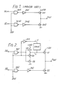
- Fig. 1 illustrates an example of a conventional semiconductor integrated circuit having an output circuit.
- the conventional semiconductor integrated circuit having a built-in substrate bias circuit is, as seen in Fig. 1, so arranged that a first gate circuit comprises a NAND circuit NA41 and an inverter IN41 and a second gate circuit comprises a NAND circuit NA42 and an inverter IN42.
- the output circuit comprises an output N-channel MOS transistor Q41 (hereinafter referred to as an N-ch Tr) which is a first output N-channel MOS transistor and an N-ch Tr Q42 which is a second output N-channel MOS transistor.
- an N-ch Tr an output N-channel MOS transistor Q41 (hereinafter referred to as an N-ch Tr) which is a first output N-channel MOS transistor and an N-ch Tr Q42 which is a second output N-channel MOS transistor.
- one input thereof is supplied with an input data signal DQ and the other input thereof is supplied with an output enabling signal DOE and, in the NAND circuit NA42, one input thereof is supplied with a complementary signal DQ of the input data signal DQ and the other input thereof is supplied with the output enabling signal DOE.
- next inverter IN41 it inverts the output of the NAND circuit NA41 and is connected to the gate of the N-ch Tr Q41 and, as for the inverter IN42, it inverts the output of the NAND circuit NA42 and is connected to the gate of the N-ch Tr Q42.
- N-ch Tr Q41 its drain is connected to a power source V DD of a positive potential and its source is connected to an output terminal of the output signal D out and, as for the N-ch Tr Q42, its drain is connected to the same output terminal of the output signal D out and its source is grounded.
- the output signal D out of a positive potential is sent out from the output terminal when the input data signal DQ is of a positive potential and the complementary signal DQ of the input data signal is of a zero potential whereas the output signal D out of a zero potential is sent out from the output terminal when the input data signal DQ is of a zero potential and the complementary signal DQ of the input data signal is of a positive potential.
- the gate potential of each of the N-ch Trs Q41, Q42 becomes the zero potential which is close to the ground potential so that the N-ch Trs Q41, Q42 are all in an OFF state and the output terminal does not output any output signal D out and is in a high impedance state.
- the hole injection in the substrate is caused by the N-ch Trs Q41, Q42 and, when the capacity of the built-in substrate bias circuit is exceeded, the substrate potential rises so as to cause a malfunction in internal circuits.
- This phenomenon is known as a malfunction caused by an ionization current.
- the magnitude of the ionization current is proportional to the current capacity of a transistor and this becomes maximum when the transistor is in a pinch-off state.
- the malfunction by the ionization current becomes worst when a high voltage is present between the drain and the source of the transistor and the gate voltage thereof is in the vicinity of the threshold voltage V TN .
- the ionization current increases exponentially in accordance with the increase of the voltage between the drain and the source.
- the main object of the present invention is to provide a semiconductor device in which the occurrence of an ionization current can be prevented even when an abnormal voltage, e.g. a negative voltage (positive voltage) is applied to the output under a high impedance state of the output terminal.
- an abnormal voltage e.g. a negative voltage (positive voltage) is applied to the output under a high impedance state of the output terminal.
- a semiconductor device comprises a first gate circuit, a second gate circuit, a first output MOS transistor and a second output MOS transistor, and a reverse bias voltage generator.
- the first gate circuit generates a first internal signal in accordance with an input data signal when an output enabling signal is at its active level data signal only when this output enabling signal is of a positive potential (negative potential), this gate circuit sends a gate signal of a positive potential (negative potential) only when the input data signal is of a positive potential (negative potential) and the output enabling signal is also of a positive potential (negative potential) and sends a gate signal of a zero potential at other times.
- the second gate circuit On receiving a complementary signal of said input data signal and the output enabling signal, the second gate circuit sends a gate signal of a positive potential (negative potential) only when the complementary signal of the input data signal is of a positive potential (negative potential) and the output enabling signal is also of a positive potential (negative potential) and sends a gate signal of a zero potential at other times.
- the first output N-(P-)channel MOS transistor its gate receives the gate signal from the first gate circuit, its drain is connected to a constant-voltage power source of a positive potential (negative potential) and its source is connected to an output terminal.
- This transistor becomes conductive and outputs an output signal of a positive potential (negative potential) only when the gate signal is of a positive potential (negative potential).
- the second output N-(P-)channel MOS transistor has a gate which receives the gate signal from the second gate circuit, a source which is grounded and a drain which is connected to the output terminal. This transistor becomes conductive and outputs an output signal of a zero potential close to the ground potential only when the gate signal is of a positive potential (negative potential).
- the reverse bias voltage generator comprises a ring oscillating circuit, a reverse bias voltage generating circuit and a switching circuit.
- the ring oscillating circuit is such that, on receiving the complementary signal of the output enabling signal, it is activated and oscillates only when the complementary signal of the output enabling signal indicative of disabling outputting of the input data signal is of a positive potential (negative potential).
- the reverse bias voltage generating circuit generates a reverse bias voltage lower (higher) than the ground potential based on the oscillation output of the ring oscillating circuit activated.
- the switching circuit is such that, on receiving the complementary signal of the output enabling signal, it supplies the reverse bias voltage from the reverse bias voltage generating circuit to the gate of the first output N-(P-)channel MOS transistor only when the complementary signal of the output enabling signal is of a positive potential (negative potential).
- Fig. 2 shows a circuit diagram of a first embodiment of the circuit used in the semiconductor integrated circuit employing a reverse bias voltage generator according to the present invention.
- the circuit of Fig. 2 is formed on a P-type semiconductor substrate and incorporates therein a substrate bias circuit.
- the first gate circuit comprises a NAND circuit NA1, an output P-channel MOS transistor Q3 (hereinafter referred to as, for example, P-ch Tr Q3) and N-ch Trs Q4, Q5 and, the second gate circuit comprises a NAND circuit NA2 and an inverter IN2.
- the output circuit comprises an N-ch Tr Q1 as a first output N-channel MOS transistor and an N-ch Tr Q2 as a second output N-channel MOS transistor.
- a reverse bias voltage generator RBVG which inputs a bias instruction signal X inverted by the inverter IN3 in response to the output enabling signal DOE, comprises a ring oscillating circuit, a reverse bias voltage generating circuit and a switching circuit, hereinafter explained in detail.
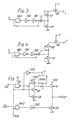
- Fig. 3 shows a circuit diagram of a first example of the reverse bias voltage generator RBVG.
- the reverse bias voltage generator RBVG forms, as shown in Fig. 3, a ring oscillating circuit with a NAND circuit NA3 and inverters IN4, IN4, a reverse bias voltage generating circuit with N-ch Trs Q6, Q7 receiving the output of the inverter IN5 through a capacitor C1 and, a switching circuit with an N-ch Tr Q8.
- One input of the NAND circuit NA1 is supplied with an input data signal DQ being of a positive potential in the presence of data and being of a zero potential in the absence of data and the other input thereof is supplied with an output enabling signal DOE being indicative of enabling outputting of the input data signal DQ only when it is of a positive potential and, one input of the NAND circuit NA2 is supplied with a complementary signal DQ of the input data signal and the other input thereof is supplied with the output enabling signal ODE, whereby these NAND circuits send out respective NAND signals.
- the P-ch Tr Q3 which receives at its gate a NAND signal from the NAND circuit NA1 has its drain connected to a constant-voltage power source V DD of a positive potential and its source connected to the drain of the N-ch Tr Q4, the gate of the N-ch Tr Q1 and the output of the reverse bias voltage generator RBVG so as to establish a gate signal Y.
- the N-ch Tr Q4 which receives at its gate the output enabling signal DOE has its source connected to the drain of the N-ch Tr Q5.
- the N-ch Tr Q5 which receives at its gate a NAND signal from the NAND circuit NA1 is grounded at its drain.
- the P-ch Tr Q3 and the N-ch Trs Q4, Q5 send to the gate of the N-ch Tr Q1 a gate signal Y of a positive potential when the input data signal DQ is of a positive potential and also the output enabling signal DOE is of a positive potential and they send a gate signal Y of a zero potential when the input data signal DQ is of a zero potential and the output enabling signal DOE is of a positive potential and, when the output enabling signal DOE is of a zero potential, the P-ch Tr Q3 and the N-ch Tr Q4 are all in an OFF state thereby providing a high impedance state.
- the inverter IN2 which inverts the output of the NAND circuit NA2 is connected to the gate of the N-ch Tr Q2. Accordingly, the inverter IN2 sends to the gate of the N-ch Tr Q2 a gate signal of a positive potential only when the complementary signal DQ of the input data signal is of a positive potential and also the output enabling signal DOE is of a positive potential and, it sends a gate signal of a zero potential at other times.
- the ring oscillating circuit in the reverse bias voltage generator RBVG is so arranged that the NAND circuit NA3, the inverters IN4 and IN5 are connected in series with one input of the NAND circuit NA3 being supplied with the bias instruction signal X and the other input of the same being connected to the output of the inverter IN5.
- the ring oscillating circuit is activated for oscillation as a consequence of the bias instruction signal X turning to a positive potential when the output enabling signal DOE is of a zero potential indicative of disabling outputting of the input data signal DQ.
- the output of the inverter IN5 is coupled to the gate as well as the drain through the capacitor C1 and the source is grounded whereas, in the N-ch Tr Q7, the source is connected to the gate as well as the drain of the N-ch Tr Q6 and the gate and the drain are connected to the source of the N-ch Tr Q8 of the switching circuit so that the oscillating output of the ring oscillating circuit activated causes the generation of a reverse bias voltage lower than the ground potential which resultant reverse bias voltage is forwarded to the source of the N-ch Tr Q8.
- the drain supplies to the gate of the N-ch Tr Q1 with the reverse bias voltage from the reverse bias voltage generating circuit as a gate signal Y only when the bias instruction signal X is of a positive potential.
- the N-ch Tr Q4 is turned ON.
- the current capacity of the reverse bias voltage generator RBVG is made smaller than that of the N-ch Trs Q4, Q5
- the potential of the gate signal Y will be in the order of -V TN .
- the N-ch Tr Q1 functions such that, with its drain being connected to the constant-voltage power source V DD of a positive potential and its source being connected to the output terminal, it becomes conductive and outputs the output signal D out of a positive potential only while the gate signal Y is of a positive potential where the input data signal DQ is of a positive potential and the output enabling signal DOE is also of a positive potential.
- the gate of the N-ch Tr Q1 is supplied from the reverse bias voltage generator RBVG a reverse bias voltage, as the gate signal Y, in the order of -V TN which is lower than the ground potential so that, unless a negative voltage greater in the absolute value than a value in the order of -2V TN is applied externally to the output terminal, the N-ch Tr Q1 will not be turned ON.
- the threshold voltage V TN is in the order of 0.5 - 0.9 V and the negative voltage -2V TN is greater in the absolute value or more negative than -1 V so that, even when a negative voltage smaller in the absolute value than -1 V is applied externally to the output terminal of the output signal D out , there is no fear of the occurrence of an ionization current due to the N-ch Tr Q1.
- the N-ch Tr Q2 receives at its gate a gate signal sent from the inverter IN2, has its source grounded and has its drain connected to the output terminal so that, only while the gate signal is of a positive potential where the complementary signal DQ of the input data signal is of a positive potential and the output enabling signal DOE is also of a positive potential, the N-ch Tr Q2 becomes conductive and outputs the output signal D out of a zero potential close to the gro8nd potential.
- Fig. 4 shows a circuit diagram of a second embodiment of the reverse bias voltage generator covered by the embodiments of the present invention.
- This second embodiment is different from the reverse bias voltage generator of the first example shown in Fig. 3 in the point that, instead of the diode connection of the N-ch Trs Q6, Q7 used in the first example, the diode connection of P-ch Trs Q9, Q10 is employed in this second embodiment.
- circuits are formed all on a P-type semiconductor substrate
- circuits according to the present invention can be formed similarly on an N-type semiconductor substrate with N-ch Trs and P-ch Trs substituted respectively for each other as shown in Fig. 5.
- the gate potential of the output N-(P-)channel MOS transistor is caused to be in a negative potential (positive potential) so that no ionization of current can occur even when a negative voltage (positive voltage) is applied to the output terminal.
- the advantage of the present invention resides in that, when there is no output enabling signal, it is possible for the gate potential of the output N-(P-)channel MOS transistor to be rendered a negative potential (positive potential) whereby the occurrence of ionization current can be effectively prevented even when a negative voltage (positive voltage) is applied to the output terminal.
Landscapes
- Engineering & Computer Science (AREA)
- Physics & Mathematics (AREA)
- Radar, Positioning & Navigation (AREA)
- Nonlinear Science (AREA)
- Electromagnetism (AREA)
- General Physics & Mathematics (AREA)
- Microelectronics & Electronic Packaging (AREA)
- Automation & Control Theory (AREA)
- Computer Hardware Design (AREA)
- Computing Systems (AREA)
- General Engineering & Computer Science (AREA)
- Mathematical Physics (AREA)
- Logic Circuits (AREA)
- Semiconductor Integrated Circuits (AREA)
- Dram (AREA)
Applications Claiming Priority (2)
| Application Number | Priority Date | Filing Date | Title |
|---|---|---|---|
| JP63242724A JPH0289357A (ja) | 1988-09-27 | 1988-09-27 | 半導体回路 |
| JP242724/88 | 1988-09-27 |
Publications (2)
| Publication Number | Publication Date |
|---|---|
| EP0361792A1 true EP0361792A1 (de) | 1990-04-04 |
| EP0361792B1 EP0361792B1 (de) | 1995-01-18 |
Family
ID=17093305
Family Applications (1)
| Application Number | Title | Priority Date | Filing Date |
|---|---|---|---|
| EP89309616A Expired - Lifetime EP0361792B1 (de) | 1988-09-27 | 1989-09-21 | Halbleitereinrichtung mit einem eine umgekehrte Vorspannung liefernden Generator |
Country Status (4)
| Country | Link |
|---|---|
| US (1) | US4996446A (de) |
| EP (1) | EP0361792B1 (de) |
| JP (1) | JPH0289357A (de) |
| DE (1) | DE68920679T2 (de) |
Families Citing this family (6)
| Publication number | Priority date | Publication date | Assignee | Title |
|---|---|---|---|---|
| IT1236534B (it) * | 1989-10-09 | 1993-03-11 | Sgs Thomson Microelectronics | Circuito di protezione da sovratensioni negative, in particolare per stadi di uscita. |
| WO1992014301A1 (en) * | 1991-02-12 | 1992-08-20 | Analog Devices, Inc. | Gain linearity correction circuit for mos circuits |
| US5245230A (en) * | 1992-03-06 | 1993-09-14 | Ohri Kul B | Low substrate injection n-channel output stage |
| US5504450A (en) * | 1993-12-08 | 1996-04-02 | At&T Corp. | High voltage components for EEPROM system |
| JPH09213073A (ja) * | 1996-02-06 | 1997-08-15 | Mitsubishi Electric Corp | 半導体集積回路 |
| US6294959B1 (en) | 1999-11-12 | 2001-09-25 | Macmillan Bruce E. | Circuit that operates in a manner substantially complementary to an amplifying device included therein and apparatus incorporating same |
Citations (3)
| Publication number | Priority date | Publication date | Assignee | Title |
|---|---|---|---|---|
| EP0042305A2 (de) * | 1980-06-18 | 1981-12-23 | Kabushiki Kaisha Toshiba | MOS-Transistor mit Durchschlagschutz |
| EP0167076A2 (de) * | 1984-06-27 | 1986-01-08 | Honeywell Inc. | Digitale Schaltung mit MESFETs |
| EP0214787A2 (de) * | 1985-08-26 | 1987-03-18 | Xerox Corporation | Treiberschaltung für eine Sammelschiene |
Family Cites Families (5)
| Publication number | Priority date | Publication date | Assignee | Title |
|---|---|---|---|---|
| JPS5632758A (en) * | 1979-08-27 | 1981-04-02 | Fujitsu Ltd | Substrate bias generating circuit |
| JPS58105563A (ja) * | 1981-12-17 | 1983-06-23 | Mitsubishi Electric Corp | 基板バイアス発生回路 |
| JPS5936427A (ja) * | 1982-08-24 | 1984-02-28 | Mitsubishi Electric Corp | 出力回路 |
| JPS59165449A (ja) * | 1983-03-10 | 1984-09-18 | Toshiba Corp | 半導体記憶装置 |
| KR890005159B1 (ko) * | 1987-04-30 | 1989-12-14 | 삼성전자 주식회사 | 백 바이어스 전압 발생기 |
-
1988
- 1988-09-27 JP JP63242724A patent/JPH0289357A/ja active Pending
-
1989
- 1989-09-21 EP EP89309616A patent/EP0361792B1/de not_active Expired - Lifetime
- 1989-09-21 DE DE68920679T patent/DE68920679T2/de not_active Expired - Fee Related
- 1989-09-27 US US07/413,336 patent/US4996446A/en not_active Expired - Lifetime
Patent Citations (3)
| Publication number | Priority date | Publication date | Assignee | Title |
|---|---|---|---|---|
| EP0042305A2 (de) * | 1980-06-18 | 1981-12-23 | Kabushiki Kaisha Toshiba | MOS-Transistor mit Durchschlagschutz |
| EP0167076A2 (de) * | 1984-06-27 | 1986-01-08 | Honeywell Inc. | Digitale Schaltung mit MESFETs |
| EP0214787A2 (de) * | 1985-08-26 | 1987-03-18 | Xerox Corporation | Treiberschaltung für eine Sammelschiene |
Also Published As
| Publication number | Publication date |
|---|---|
| EP0361792B1 (de) | 1995-01-18 |
| DE68920679D1 (de) | 1995-03-02 |
| DE68920679T2 (de) | 1995-05-18 |
| US4996446A (en) | 1991-02-26 |
| JPH0289357A (ja) | 1990-03-29 |
Similar Documents
| Publication | Publication Date | Title |
|---|---|---|
| US7768308B2 (en) | Level shift circuit | |
| US20220321126A1 (en) | Level shifter circuit and method of operating the same | |
| KR100206870B1 (ko) | 정전 방전 및 래치 업 방지회로 | |
| US5990705A (en) | CMOS I/O circuit with high-voltage input tolerance | |
| KR0122246Y1 (ko) | 레벨변환회로 | |
| KR100318298B1 (ko) | 반도체장치 | |
| US5327072A (en) | Regulating circuit for a substrate bias voltage generator | |
| EP0361792B1 (de) | Halbleitereinrichtung mit einem eine umgekehrte Vorspannung liefernden Generator | |
| US4672241A (en) | High voltage isolation circuit for CMOS networks | |
| US6078197A (en) | Output driver circuit utilizing floating wells | |
| TW201431290A (zh) | 輸出緩衝器 | |
| KR100242987B1 (ko) | 5v 톨러런트 입출력 회로 | |
| TWI641219B (zh) | 電源啟動控制電路以及輸入/出控制電路 | |
| JP2703890B2 (ja) | 半導体集積回路 | |
| US6292093B1 (en) | Multi-bit comparator | |
| US6326835B1 (en) | Input/output circuit for semiconductor integrated circuit device | |
| KR100451421B1 (ko) | 전원 전압 레귤레이션 회로 | |
| KR0150227B1 (ko) | 입력 회로 | |
| KR100318465B1 (ko) | 반도체장치의접지전위클램프회로 | |
| KR100221612B1 (ko) | 씨엠오에스 출력버퍼의 바이어스 조정 회로 | |
| KR960000899B1 (ko) | 고전압 선택회로 및 그를 포함하는 데이타 출력버퍼 | |
| KR100277866B1 (ko) | 반도체 소자의 출력 드라이버 | |
| JPH1174772A (ja) | 電源電圧切換回路 | |
| US5412264A (en) | Signal input/output circuit for semiconductor integrated circuit | |
| KR910009556B1 (ko) | 백 바이어스 전압발생회로 |
Legal Events
| Date | Code | Title | Description |
|---|---|---|---|
| PUAI | Public reference made under article 153(3) epc to a published international application that has entered the european phase |
Free format text: ORIGINAL CODE: 0009012 |
|
| 17P | Request for examination filed |
Effective date: 19890929 |
|
| AK | Designated contracting states |
Kind code of ref document: A1 Designated state(s): DE FR GB |
|
| 17Q | First examination report despatched |
Effective date: 19930826 |
|
| GRAA | (expected) grant |
Free format text: ORIGINAL CODE: 0009210 |
|
| AK | Designated contracting states |
Kind code of ref document: B1 Designated state(s): DE FR GB |
|
| REF | Corresponds to: |
Ref document number: 68920679 Country of ref document: DE Date of ref document: 19950302 |
|
| ET | Fr: translation filed | ||
| PG25 | Lapsed in a contracting state [announced via postgrant information from national office to epo] |
Ref country code: GB Effective date: 19950921 |
|
| PLBE | No opposition filed within time limit |
Free format text: ORIGINAL CODE: 0009261 |
|
| STAA | Information on the status of an ep patent application or granted ep patent |
Free format text: STATUS: NO OPPOSITION FILED WITHIN TIME LIMIT |
|
| 26N | No opposition filed | ||
| GBPC | Gb: european patent ceased through non-payment of renewal fee |
Effective date: 19950921 |
|
| PG25 | Lapsed in a contracting state [announced via postgrant information from national office to epo] |
Ref country code: FR Effective date: 19960531 |
|
| PG25 | Lapsed in a contracting state [announced via postgrant information from national office to epo] |
Ref country code: DE Effective date: 19960601 |
|
| REG | Reference to a national code |
Ref country code: FR Ref legal event code: ST |