EP0167275A2 - Dispositif de mémoire semi-conductrice - Google Patents
Dispositif de mémoire semi-conductrice Download PDFInfo
- Publication number
- EP0167275A2 EP0167275A2 EP85303838A EP85303838A EP0167275A2 EP 0167275 A2 EP0167275 A2 EP 0167275A2 EP 85303838 A EP85303838 A EP 85303838A EP 85303838 A EP85303838 A EP 85303838A EP 0167275 A2 EP0167275 A2 EP 0167275A2
- Authority
- EP
- European Patent Office
- Prior art keywords
- pulse width
- memory device
- semiconductor memory
- signal
- write
- Prior art date
- Legal status (The legal status is an assumption and is not a legal conclusion. Google has not performed a legal analysis and makes no representation as to the accuracy of the status listed.)
- Granted
Links
Images


Classifications
-
- G—PHYSICS
- G11—INFORMATION STORAGE
- G11C—STATIC STORES
- G11C11/00—Digital stores characterised by the use of particular electric or magnetic storage elements; Storage elements therefor
- G11C11/21—Digital stores characterised by the use of particular electric or magnetic storage elements; Storage elements therefor using electric elements
- G11C11/34—Digital stores characterised by the use of particular electric or magnetic storage elements; Storage elements therefor using electric elements using semiconductor devices
-
- G—PHYSICS
- G11—INFORMATION STORAGE
- G11C—STATIC STORES
- G11C8/00—Arrangements for selecting an address in a digital store
-
- G—PHYSICS
- G11—INFORMATION STORAGE
- G11C—STATIC STORES
- G11C11/00—Digital stores characterised by the use of particular electric or magnetic storage elements; Storage elements therefor
- G11C11/21—Digital stores characterised by the use of particular electric or magnetic storage elements; Storage elements therefor using electric elements
- G11C11/34—Digital stores characterised by the use of particular electric or magnetic storage elements; Storage elements therefor using electric elements using semiconductor devices
- G11C11/40—Digital stores characterised by the use of particular electric or magnetic storage elements; Storage elements therefor using electric elements using semiconductor devices using transistors
-
- G—PHYSICS
- G11—INFORMATION STORAGE
- G11C—STATIC STORES
- G11C7/00—Arrangements for writing information into, or reading information out from, a digital store
- G11C7/22—Read-write [R-W] timing or clocking circuits; Read-write [R-W] control signal generators or management
-
- G—PHYSICS
- G11—INFORMATION STORAGE
- G11C—STATIC STORES
- G11C8/00—Arrangements for selecting an address in a digital store
- G11C8/18—Address timing or clocking circuits; Address control signal generation or management, e.g. for row address strobe [RAS] or column address strobe [CAS] signals
Definitions
- the present invention relates to a memory device using semiconductors, particularly bipolar type semiconductors, more particularly a semiconductor memory device having a pulse width control circuit for preventing erroneous operation of its write circuit.
- a semiconductor memory device usually cannot perform a write operation unless the pulse width of the write enable signal is greater than a certain length.
- One of the exceptions is just after a change of address. At such times, the write operation can be carried out by a write enable signal having a relatively short pulse width. Consequently an erroneous write operation may be caused just after a change of address by noise.
- JP-A-53-114651 discloses a device with a pulse width control circuit for inhibiting the passage of write enable signals having a pulse width smaller than a predetermined pulse width. This circuit only permits the passage of a write enable signal having a pulse width greater than a predetermined length and inhibits the passage of signals having less than the predetermined pulse width.
- This pulse width control circuit prevents erroneous write operations due to noise.
- the circuit requires a certain processing time and a minimum pulse width of the write enable signal to effect the write operation. As a result, the write cycle time is disadvantageously increased.
- such a semiconductor memory device also includes an address change detecting means for detecting a change of address of memory cells and delivering an output signal for a predetermined period of time upon the detection of a change of address, and the pulse width control means inhibits the passage of the write enable signals only during said predetermined period.
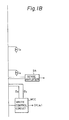
- Figure 1 shows a semiconductor memory device of the prior art.
- MC 00 through MC11 are memory cells of an emitter-coupled logic (ECL) type
- WL 9 and WL 1 are word lines
- Tr 2 through Tr 5 are bitline selection transistors
- Tr 6 through Tr 9 are read/write control transistors
- SA is a sense amplifier
- WCC is a write control circuit
- PWC is a pulse-width control circuit
- I H and 1 0 are current sources.
- Each of memory cells MC 00 through MC 11 includes two multi emitter transistors Q1 and Q2, as typically shown by MC 00 .
- the word driver WD O and bit line selection transistors Tr 2 and Tr 3 are used to address the memory cell MC 00 .
- a write enable signal WE is then supplied to the write control circuit.
- One of the control signals D 0 and D 1 become “0" and the other "1” in accordance with the write data D(in). Consequently the write operation of the memory cell MC 00 is effected.
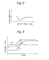
- the write enable signal is applied after a setup time t(SA) from the change of address.
- the write enable signal must have a pulse width greater than a certain magnitude. This certain magnitude which is necessary for the write operation varies in accordance with the setup time t(SA).
- Figure 2 shows the relationship between the setup time t(SA) of the write enable signal and the minimum necessary pulse width. In Figure 2, the ordinate represents the minimum necessary pulse width PW, and the abscissa represents the setup time t(SA). As clear from Figure 2, a write operation is possible just after the change of address even with short pulse width. As the setup time t(SA) becomes longer, however, the write operation cannot be effected unless the pulse width is greater than a certain magnitude.
- Figure 3 thus shows the variations of the collector voltage of the these transistors Q1 and Q2 before and after the change of address.
- (1) represents the collector voltage of the transistors Q1, (2) the collector voltage of the transistors Q2, and (3) the voltage of the word line WL 0 .
- the collector voltage (2) rises up gradually from H 1 to H 2 .
- the collector voltage (1) of the transistor Q1 rises up rapidly from L 1 in an "overdamping" state and then stabilizes at L 2 .
- the write operation can be effected by means of a write enable signal having a short pulse width just after the change of address, it can also be effected by noise, resulting in an erroneous write operation.
- Such a pulse width control circuit PWC is shown at the centre bottom of Figure 1.
- the circuit includes a delay element D, an AND gate G10, and a pulse width extension circuit PWE which extends the pulse width of the output of the AND gate G10 to a certain magnitude.
- the output of the AND gate G10 appears only when input signals are simultaneously applied on its two input terminals. Accordingly, when the pulse width of the write enable signal WE is smaller than the delay time of the delay element D, the passage of the write enable signal is inhibited by the AND gate G10.
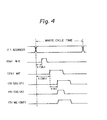
- Figure 4 shows signal waveforms at individual points of the pulse width control circuit PWC of Figure l.
- (1) represents the state of change of the address
- (3) an output signal of the delay element D (4) an output signal of the AND gate G10
- an output signal of the pulse width extension circuit PWE as an internal write enable signal WE(INT) whose pulse width is extended to the pulse width of original write enable signal WE.
- the pulse width of the write enable signal WE is short ( Figure 4 - 2a)
- no output signal appears at the output of the AND gate G10 therefore, no internal write enable signal WE(INT) appears.
- an internal write enable signal WE(INT) is delivered from the AND gate G10, whereby the write operation is effected.
- the above-described circuit PWC may be used to prevent erroneous write operations caused by noise just after the change of address.
- the circuit requires the delay time caused at the delay element D in addition to a minimum pulse duration. This results in an increased write cycle time.
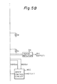
- Figure 5 illustrates a semiconductor memory device of an embodiment of the present invention.
- MC 00' MC 01 , MC 10 , and MC 11 are memory cells of the EC L type
- WL 0 and WL 1 are word lines
- BL 00 , BL 01' B L 10' and BL 11 are bit lines.
- the word lines WL 0 and WL 1 are connected to one of the emitters of multi emitter type transistors TR 0 and Tr 1 , respectively.
- WD O and WD 1 are word drivers which receive input signals from an address decoder (not shown in Figure 5).
- the bit lines BL 00 , BL 01' BL 10' and BL 11 are connected to current sources via the bit line selection transistors Tr 2 , Tr 3 , Tr 4 , and Tr 5 , respectively. Furthermore, the bit lines BL 00 , BL 01' BL 10 , and BL 11 are connected to a sense amplifier SA via the transistors TR 6 , TR 7 , Tr 8 , and Trg, respectively. The bases of the transistors Tr 6 through Tr 9 are connected to a write control circuit WCC. These transistors Tr 6 through Tr 9 are driven by the control signals D 0 and D 1 delivered from the write control circuit WCC.
- the write control circuit WCC generates the control signals DO and D 1 , one being the logical level “1" and the other "0", in accordance with write data D(in).
- a pulse width control circuit PWC supplies this write control circuit WCC with an internal write enable signal WE(INT).
- the pulse width control circuit PWC operates so as to allow the passage of a write enable signal WE applied externally only when the signal WE has pulse width greater than a predetermined magnitude. Furthermore, this circuit PWC itself selects whether to enable or inhibit such an operation depending upon the address change.
- the pulse width control circuit PWC including, for example, an inverter G1, NOR gate G2, and OR gate G3, which operates in the manner of a negative logic.
- the write enable signal WE is directly applied to one input terminal of the OR gate G3 and is applied to the other input terminal of the OR gate G3 after being delayed by the inverter G1 and the NOR gate G3.
- the other input terminal of the NOR gate G2 is connected to the other emitter of the multi emitter transistors TR O and Tr l . Therefore, when a change of memory address is effected, it receives a signal AD of a logical level "1" (Low level) for a predetermined period from the time of the change. Consequently, the NOR gate G2 is opened for the predetermined period after the change, whereby pulse width control of the write enable signal WE is effected.
- the signal AD becomes the logical level "0", (High level) whereupon the NOR gate G2 is closed and its output is kept at the logical level "1". Accordingly, the write enable signal WE is directly delivered as the internal write enable signal WE(INT).
- Figure 6 shows an embodiment of the pulse width control circuit PWC in Figure 5, constituted in the form of an ECL. This circuit corresponds exactly to that shown in Figure 5, therefore, operates in the manner of a negative logic.
- IN i is an input terminal for the write enable signal WE
- IN 2 is an input terminal for the signal AD
- OUT is an output terminal where the internal write enable signal WE(INT) appears
- V R1 is a reference voltage.
- the signal AD becomes the "L" level for a certain period due to the time lag between the rise and fall of the outputs of the transistors TR O and Tr l .
- the signal AD is the "L" level
- pulse width control is effected. That is, when the write enable signal WE is applied to the input terminal IN 1 , a signal P delayed with respect to the signal WE is generated. As a result, a logical product signal of this delayed signal P and the write enable signal WE is delivered from the output terminal OUT as the internal write enable signal WE(INT). It is also possible to extend the pulse width of this logical product signal by integration and adopt it as the internal write enable signal WE(INT).
- control signals D 0 and D 1 having inverse logics are formed in accordance with the write data D(in) .
- These control signals D 0 and D 1 are applied to the bases of the transistors Tr 6 through Trg. By this, the data D(in) is written into the addressed memory cell.
- the pulse width control circuit PWC is not limited to the constitution described above.
- Figure 10 shows another embodiment of the pulse width control circuit PWC. This embodiment is somewhat more simplified compared with circuit of Figure 6, but is also constituted in the form of an ECL, operating in the manner of a negative logic.
- IN 1 , IN 2 , and OUT are terminals the same as those shown in Figure 6, and VR 1 and VR 2 are reference voltages.
- the transistors TR 11 turns on and the delayed signal P is kept at the "L” level.
- the write enable signal WE is directly output as the internal write enable signal WE(INT).
- TTL transistor-transistor logic
- the pulse width control circuit PWC may be constituted by a positive logic circuit instead of a negative logic circuit described above.
- Figure 11 shows such a circuit PWC, including an inverter G4, a NAND gate G5, and an AND gate G6.
- Figures 12A and 12B show a write enable signal WE, an internal write enable signal WE(INT), and a delayed signal P in the circuit PWC of Figure 11, Figure 12A showing the case just after the change of address where pulse width control is effected and Figure 12B showing the case after a certain time elapses from the change of address where pulse width control is not effected.
- the signal AD taken out from the emitters of the transistors TR and TR 1 was directly supplied to the pulse width control circuit PWC.
- the signal may be supplied via the circuit PWE of Figure 11, which extends the duration of the signal AD.
- pulse width control of the write enable signal possible only in a predetermined period just after the change of address.
- problems such as the pulse width of the write enable signal becoming too large or the write cycle time becoming too long are eliminated.
- the write operation is enabled even by a write enable signal having a short pulse width just after the change of address. Consequently, erroneous operations readily occur. If pulse width control is always effected so as to prevent such erroneous operations, the continuous delay as shown by PW 2 in Figure 13 increases the pulse width of the write enable signal, i.e., increases the write cycle time.
- pulse width control is effected only in a predetermined period from the change of address which is very first portion of the each address cycle. Therefore, the delay time due to the pulse width control circuit function does not affect the whole cycle time. During this pulse width control, a write operation cannot be effected by a write enable signal having a short pulse width. Therefore, no erroneous write operation due to noise occurs.
Landscapes
- Engineering & Computer Science (AREA)
- Microelectronics & Electronic Packaging (AREA)
- Computer Hardware Design (AREA)
- Static Random-Access Memory (AREA)
Applications Claiming Priority (2)
| Application Number | Priority Date | Filing Date | Title |
|---|---|---|---|
| JP108516/84 | 1984-05-30 | ||
| JP59108516A JPS60253091A (ja) | 1984-05-30 | 1984-05-30 | 半導体記憶装置 |
Publications (3)
| Publication Number | Publication Date |
|---|---|
| EP0167275A2 true EP0167275A2 (fr) | 1986-01-08 |
| EP0167275A3 EP0167275A3 (en) | 1986-12-30 |
| EP0167275B1 EP0167275B1 (fr) | 1991-05-29 |
Family
ID=14486769
Family Applications (1)
| Application Number | Title | Priority Date | Filing Date |
|---|---|---|---|
| EP85303838A Expired - Lifetime EP0167275B1 (fr) | 1984-05-30 | 1985-05-30 | Dispositif de mémoire semi-conductrice |
Country Status (5)
| Country | Link |
|---|---|
| US (1) | US4802131A (fr) |
| EP (1) | EP0167275B1 (fr) |
| JP (1) | JPS60253091A (fr) |
| KR (1) | KR900000051B1 (fr) |
| DE (1) | DE3582960D1 (fr) |
Cited By (5)
| Publication number | Priority date | Publication date | Assignee | Title |
|---|---|---|---|---|
| EP0311102A3 (en) * | 1987-10-09 | 1989-09-27 | Kabushiki Kaisha Toshiba | Semiconductor ic including circuit for preventing erroneous operation caused by power source noise |
| EP0233550A3 (en) * | 1986-02-04 | 1990-05-23 | Fujitsu Limited | A time delay circuit for a semiconductor device |
| EP0329177B1 (fr) * | 1988-02-18 | 1994-06-15 | Kabushiki Kaisha Toshiba | Dispositif de mémoire à semi-conducteurs pouvant supprimer une faute d'opération due à un bruit d'alimentation |
| EP0624878A3 (fr) * | 1987-12-28 | 1995-02-15 | Tokyo Shibaura Electric Co | Circuit intégré à semi-conducteurs. |
| EP0405812B1 (fr) * | 1989-06-20 | 1997-08-27 | Texas Instruments Incorporated | Circuit d'attaque |
Families Citing this family (11)
| Publication number | Priority date | Publication date | Assignee | Title |
|---|---|---|---|---|
| JPH0612631B2 (ja) * | 1986-10-17 | 1994-02-16 | 日本電気株式会社 | 半導体メモリ |
| JP2585602B2 (ja) * | 1987-06-10 | 1997-02-26 | 株式会社日立製作所 | 半導体記憶装置 |
| JP2701030B2 (ja) * | 1987-10-09 | 1998-01-21 | 株式会社日立製作所 | 高速記憶装置の書込制御回路 |
| JP2941817B2 (ja) * | 1988-09-14 | 1999-08-30 | 株式会社日立製作所 | ベクトル処理装置 |
| DE4023404C2 (de) * | 1990-07-23 | 1996-05-15 | Castolin Sa | Verwendung einer abschmelzbaren Elektrode |
| US5574866A (en) * | 1993-04-05 | 1996-11-12 | Zenith Data Systems Corporation | Method and apparatus for providing a data write signal with a programmable duration |
| US5826063A (en) * | 1993-11-08 | 1998-10-20 | Cirrus Logic, Inc. | Apparatus and method for programming the setup, command and recovery time periods within a transaction cycle |
| EP0709774A1 (fr) * | 1994-10-27 | 1996-05-01 | STMicroelectronics S.r.l. | Procédé et dispositif pour détecter un défaut d'un signal d'horloge pour des dispositifs électroniques à microprocesseur avec éléments de mémoire |
| US5815463A (en) * | 1997-06-12 | 1998-09-29 | Etron Technology, Inc | Flexible time write operation |
| KR100333703B1 (ko) * | 1999-06-30 | 2002-04-24 | 박종섭 | 동기식 디램의 데이터 스트로브 버퍼 |
| US6928026B2 (en) | 2002-03-19 | 2005-08-09 | Broadcom Corporation | Synchronous global controller for enhanced pipelining |
Family Cites Families (9)
| Publication number | Priority date | Publication date | Assignee | Title |
|---|---|---|---|---|
| JPS6057156B2 (ja) * | 1978-05-24 | 1985-12-13 | 株式会社日立製作所 | 半導体メモリ装置 |
| US4337525A (en) * | 1979-04-17 | 1982-06-29 | Nippon Electric Co., Ltd. | Asynchronous circuit responsive to changes in logic level |
| JPS5668990A (en) * | 1979-11-08 | 1981-06-09 | Nec Corp | Memory circuit |
| JPS55142487A (en) * | 1979-04-25 | 1980-11-07 | Hitachi Ltd | Bipolar memory circuit |
| JPS5634186A (en) * | 1979-08-29 | 1981-04-06 | Hitachi Ltd | Bipolar memory circuit |
| US4355377A (en) * | 1980-06-30 | 1982-10-19 | Inmos Corporation | Asynchronously equillibrated and pre-charged static ram |
| JPS5835783A (ja) * | 1981-08-24 | 1983-03-02 | Fujitsu Ltd | 半導体メモリ |
| JPS6052520B2 (ja) * | 1981-12-29 | 1985-11-19 | 富士通株式会社 | 半導体記憶装置 |
| JPS58169383A (ja) * | 1982-03-30 | 1983-10-05 | Fujitsu Ltd | 半導体記憶装置 |
-
1984
- 1984-05-30 JP JP59108516A patent/JPS60253091A/ja active Granted
-
1985
- 1985-05-29 KR KR1019850003732A patent/KR900000051B1/ko not_active Expired
- 1985-05-30 DE DE8585303838T patent/DE3582960D1/de not_active Expired - Lifetime
- 1985-05-30 EP EP85303838A patent/EP0167275B1/fr not_active Expired - Lifetime
-
1988
- 1988-02-08 US US07/152,997 patent/US4802131A/en not_active Expired - Fee Related
Cited By (7)
| Publication number | Priority date | Publication date | Assignee | Title |
|---|---|---|---|---|
| EP0233550A3 (en) * | 1986-02-04 | 1990-05-23 | Fujitsu Limited | A time delay circuit for a semiconductor device |
| EP0311102A3 (en) * | 1987-10-09 | 1989-09-27 | Kabushiki Kaisha Toshiba | Semiconductor ic including circuit for preventing erroneous operation caused by power source noise |
| US4896056A (en) * | 1987-10-09 | 1990-01-23 | Kabushiki Kaisha Toshiba | Semiconductor IC including circuit for preventing erroneous operation caused by power source noise |
| EP0624878A3 (fr) * | 1987-12-28 | 1995-02-15 | Tokyo Shibaura Electric Co | Circuit intégré à semi-conducteurs. |
| EP0322901B1 (fr) * | 1987-12-28 | 1995-05-17 | Kabushiki Kaisha Toshiba | Circuit intégré à semi-conducteurs |
| EP0329177B1 (fr) * | 1988-02-18 | 1994-06-15 | Kabushiki Kaisha Toshiba | Dispositif de mémoire à semi-conducteurs pouvant supprimer une faute d'opération due à un bruit d'alimentation |
| EP0405812B1 (fr) * | 1989-06-20 | 1997-08-27 | Texas Instruments Incorporated | Circuit d'attaque |
Also Published As
| Publication number | Publication date |
|---|---|
| DE3582960D1 (de) | 1991-07-04 |
| EP0167275A3 (en) | 1986-12-30 |
| KR850008756A (ko) | 1985-12-21 |
| JPS60253091A (ja) | 1985-12-13 |
| US4802131A (en) | 1989-01-31 |
| KR900000051B1 (ko) | 1990-01-18 |
| EP0167275B1 (fr) | 1991-05-29 |
| JPH0453036B2 (fr) | 1992-08-25 |
Similar Documents
| Publication | Publication Date | Title |
|---|---|---|
| EP0167275A2 (fr) | Dispositif de mémoire semi-conductrice | |
| US4337523A (en) | Bipolar memory circuit | |
| US5532961A (en) | Semiconductor memory device having extended data out function | |
| EP0618588B1 (fr) | Méthode et circuit pour améliorer le marge de bruit de signaux de temporisation dans une mémoire DRAM | |
| US5463585A (en) | Semiconductor device incorporating voltage reduction circuit therein | |
| US4766572A (en) | Semiconductor memory having a bypassable data output latch | |
| US5500820A (en) | Semiconductor memory device | |
| US4563754A (en) | Static-type random-access memory device | |
| US4751683A (en) | Static semiconductor memory device comprising word lines each operating at three different voltage levels | |
| EP0096421B1 (fr) | Dispositif de mémoire statique comprenant un détecteur de signal de transition | |
| US4893276A (en) | Output circuit of a static random access memory circuit | |
| US5268863A (en) | Memory having a write enable controlled word line | |
| US4516224A (en) | Semiconductor memory | |
| EP0144836A2 (fr) | Circuit d'impulsion de transition d'adresse | |
| US5719812A (en) | Semiconductor memory including bit line reset circuitry and a pulse generator having output delay time dependent on type of transition in an input signal | |
| US4458338A (en) | Circuit for checking memory cells of programmable MOS-integrated semiconductor memories | |
| US5936897A (en) | Semiconductor storage device capable of fast writing operation | |
| US4797573A (en) | Output circuit with improved timing control circuit | |
| US4809230A (en) | Semiconductor memory device with active pull up | |
| US4520462A (en) | Semiconductor memory device | |
| US4463448A (en) | Semiconductor memory device | |
| US5229966A (en) | Current control circuit for dynamic memory | |
| US5136186A (en) | Glitch free power-up for a programmable array | |
| US4409674A (en) | Semiconductor memory | |
| US4119871A (en) | Function generator for the production of a voltage across a node to which are connected flip-flops which are arranged in bit lines of a MOS memory and consists of MOS transistors |
Legal Events
| Date | Code | Title | Description |
|---|---|---|---|
| PUAI | Public reference made under article 153(3) epc to a published international application that has entered the european phase |
Free format text: ORIGINAL CODE: 0009012 |
|
| AK | Designated contracting states |
Designated state(s): DE FR GB |
|
| PUAL | Search report despatched |
Free format text: ORIGINAL CODE: 0009013 |
|
| AK | Designated contracting states |
Kind code of ref document: A3 Designated state(s): DE FR GB |
|
| 16A | New documents despatched to applicant after publication of the search report | ||
| 17P | Request for examination filed |
Effective date: 19870618 |
|
| 17Q | First examination report despatched |
Effective date: 19890120 |
|
| GRAA | (expected) grant |
Free format text: ORIGINAL CODE: 0009210 |
|
| AK | Designated contracting states |
Kind code of ref document: B1 Designated state(s): DE FR GB |
|
| ET | Fr: translation filed | ||
| REF | Corresponds to: |
Ref document number: 3582960 Country of ref document: DE Date of ref document: 19910704 |
|
| PLBE | No opposition filed within time limit |
Free format text: ORIGINAL CODE: 0009261 |
|
| STAA | Information on the status of an ep patent application or granted ep patent |
Free format text: STATUS: NO OPPOSITION FILED WITHIN TIME LIMIT |
|
| 26N | No opposition filed | ||
| PGFP | Annual fee paid to national office [announced via postgrant information from national office to epo] |
Ref country code: FR Payment date: 19960510 Year of fee payment: 12 |
|
| PGFP | Annual fee paid to national office [announced via postgrant information from national office to epo] |
Ref country code: GB Payment date: 19960521 Year of fee payment: 12 |
|
| PGFP | Annual fee paid to national office [announced via postgrant information from national office to epo] |
Ref country code: DE Payment date: 19960528 Year of fee payment: 12 |
|
| PG25 | Lapsed in a contracting state [announced via postgrant information from national office to epo] |
Ref country code: GB Effective date: 19970530 |
|
| GBPC | Gb: european patent ceased through non-payment of renewal fee |
Effective date: 19970530 |
|
| PG25 | Lapsed in a contracting state [announced via postgrant information from national office to epo] |
Ref country code: FR Free format text: LAPSE BECAUSE OF NON-PAYMENT OF DUE FEES Effective date: 19980130 |
|
| PG25 | Lapsed in a contracting state [announced via postgrant information from national office to epo] |
Ref country code: DE Free format text: LAPSE BECAUSE OF NON-PAYMENT OF DUE FEES Effective date: 19980203 |
|
| REG | Reference to a national code |
Ref country code: FR Ref legal event code: ST |