EP0167959B1 - Traitement pour registres de vecteur de calculateur - Google Patents
Traitement pour registres de vecteur de calculateur Download PDFInfo
- Publication number
- EP0167959B1 EP0167959B1 EP85108148A EP85108148A EP0167959B1 EP 0167959 B1 EP0167959 B1 EP 0167959B1 EP 85108148 A EP85108148 A EP 85108148A EP 85108148 A EP85108148 A EP 85108148A EP 0167959 B1 EP0167959 B1 EP 0167959B1
- Authority
- EP
- European Patent Office
- Prior art keywords
- address
- read
- vector register
- vector
- write
- Prior art date
- Legal status (The legal status is an assumption and is not a legal conclusion. Google has not performed a legal analysis and makes no representation as to the accuracy of the status listed.)
- Expired - Lifetime
Links
Images


Classifications
-
- G—PHYSICS
- G06—COMPUTING OR CALCULATING; COUNTING
- G06F—ELECTRIC DIGITAL DATA PROCESSING
- G06F9/00—Arrangements for program control, e.g. control units
- G06F9/06—Arrangements for program control, e.g. control units using stored programs, i.e. using an internal store of processing equipment to receive or retain programs
- G06F9/30—Arrangements for executing machine instructions, e.g. instruction decode
- G06F9/30003—Arrangements for executing specific machine instructions
- G06F9/30007—Arrangements for executing specific machine instructions to perform operations on data operands
- G06F9/30032—Movement instructions, e.g. MOVE, SHIFT, ROTATE, SHUFFLE
-
- G—PHYSICS
- G06—COMPUTING OR CALCULATING; COUNTING
- G06F—ELECTRIC DIGITAL DATA PROCESSING
- G06F15/00—Digital computers in general; Data processing equipment in general
- G06F15/76—Architectures of general purpose stored program computers
- G06F15/80—Architectures of general purpose stored program computers comprising an array of processing units with common control, e.g. single instruction multiple data processors
- G06F15/8053—Vector processors
- G06F15/8076—Details on data register access
-
- G—PHYSICS
- G06—COMPUTING OR CALCULATING; COUNTING
- G06F—ELECTRIC DIGITAL DATA PROCESSING
- G06F9/00—Arrangements for program control, e.g. control units
- G06F9/06—Arrangements for program control, e.g. control units using stored programs, i.e. using an internal store of processing equipment to receive or retain programs
- G06F9/30—Arrangements for executing machine instructions, e.g. instruction decode
- G06F9/30003—Arrangements for executing specific machine instructions
- G06F9/30007—Arrangements for executing specific machine instructions to perform operations on data operands
- G06F9/30036—Instructions to perform operations on packed data, e.g. vector, tile or matrix operations
-
- G—PHYSICS
- G06—COMPUTING OR CALCULATING; COUNTING
- G06F—ELECTRIC DIGITAL DATA PROCESSING
- G06F9/00—Arrangements for program control, e.g. control units
- G06F9/06—Arrangements for program control, e.g. control units using stored programs, i.e. using an internal store of processing equipment to receive or retain programs
- G06F9/30—Arrangements for executing machine instructions, e.g. instruction decode
- G06F9/30098—Register arrangements
Definitions
- the present invention relates to high speed digital processors, and more particularly to computing machines adapted for vector processing.
- US-A-4,128,880 describes an example of such vector processing apparatus.
- vector processing in a computer is achieved by means of a plurality of vector registers 20 (V0-V7), a plurality of independent fully segmented vector functional units and means for controlling the operation of the vector registers, including fan-outs 22 and 23 for selecting a signal, a data path 21 and a memory 12.
- Each of vector registers V0-V7 has 64 individual elements, each of which can hold a 64 bit word.
- element data in the register 20 are sequentially stored in the memory 12 via the fan-out 22 and data path 21 by store instructions, and a portion of the element data in the memory 12 are then loaded to the register V1 via the fan-out 22.
- the element data in the register V0 is sent to the shift functional unit via the fan-out 23 by a shift instruction.
- the shift functional unit can perform a shift in accordance with a shift quantity designated by the instruction.
- the output of the shift functional unit is moved, shifted by one word, to the vector register V1 via the fan-out 23.
- the desired movement of element data is accomplished by repeating this shift operation. Accordingly, since both techniques need either the memory 12 or the shift functional unit, the performance of element data movement becomes slow.
- the next instruction needs the memory 12 and/or the shift functional unit, a conflict in using these devices has occurred.
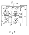
- a computer includes vector registers 100 and 101, read address registers 110 and 111, write address registers 120 and 121, read address selectors 130 and 131, write address selectors 140 and 141, and an input selector 200 for selecting input element data.
- a plurality of vector registers e.g., two vector registers 100 and 101 in this embodiment, hold a plurality of elements of an ordered set of data, respectively.
- Each of the registers 100 and 101 stores data loaded from a main storage or the result of an arithmetic operation from an ALU.
- An instruction will include the operation code (OP) and four operands R1, R2, R3 and R4.
- the operand R1 designates the destination vector register number
- the operand R3 designates the source vector register number.
- the operand R2 designates the write starting address of the destination vector register designated by the operand R1. If not necessary to designate the write starting address, it is not used.
- the operand R4 designates the read starting address of the source vector register designated by the operand R3. If not necessary, it is not used.
- the operation of designating read starting address for the source vector address 100 is as follows.
- the operand R4 is sent to the address selector 130.
- "0" is set into the selector 130.
- the output from the selector 130 is stored into a read address register 110 when the operation code designates the element data move instruction and the operand R3, i.e., the source vector register number, designates the vector register 100.
- the operand R2 is sent to the write address selector 141.
- "0" is sent to the selector 141.
- the output from the selector 141 is stored into the write address register 121 when the operation code designates an element data move instruction and the operand R1, i.e., the destination vector register number, designates the vector register 101.
- the operand R4 is sent into the read address selector 131.
- "0" is sent into the selector 131.
- the output from the selector 131 is stored into the read address register 111 when the operation code designates an element data move instruction and the operand R3, i.e., the source vector register number, designates the vector register 101.
- the operand R2 is sent to the write address selector 140.
- "0" is sent into the selector 140.
- the output from the selector 140 is stored into the write address register 120 when the operation code designates the element data move instruction and the operand R1, i.e., the destination vector register number, shows the vector register 100.
- the maximum number of element data capable of being stored in the vector registers 100 and 101 is 64. If 32 element data are moved from the vector register 100 to the register 101, the vector length register (not shown in the Figure) holds the vector length number "32" in accordance with an instruction indicating the vector length.
- the operand R3, representing the source vector register number designates the vector register 100
- the operand R1, representing the destination vector register number designates the vector register 101
- the operand R4 representing the read starting address for the vector register 100 designates the number "32”.
- the read starting address designated by the instruction is given to read address selector 130.
- the address selected by the selector 130 is stored in the read address register 110.
- "0" is stored in the write address register 121 via the address selector 141.
- the vector register 100 sends the element data from the location of the register 100 designated by the address register 110 to the selector 200.
- the read address register 110 has "1" increment function to read the element data in sequentially, and counts the location 33 following location 32.
- the element data stored in the vector register 100 is read out, and sent to the selector 200.
- the selector 200 selects the element data read out from the vector register 100 for input to the vector register 101.
- the vector register 101 starts to store the element data.
- the write address register 121 has a "1" increment function for writing the element data in sequence like the read address register 110, and counts the location 1 following location 0.
- the element data is provided from the selector 200 to the location of the vector register 101 designated by the counted location. This operation is complete when the number of element data moved reaches "32", that is, the number is equal to the designated vector length.
- FIG. 5 An example of a portion of the element data input selector 200 is illustrated in Figure 5.
- the operation code is provided to the decoder 400 and is judged as to whether or not the code designates an element data move instruction.
- the operand R3 is decoded by a decoder 402, and the decoded result designates the source vector register to a decoder 400.
- the gates 500, 510, 420, 530 and 540 select one of the outputs from vector registers 100 and 101, the main storage (not shown in the Figure) and the ALU (not shown in the Figure).
- the read address register 110 functions to count the number of the vector length designation in sequence so that the next location 0 is designated when the location of the vector register 100 is "63".
- the source vector register number R3 designates the vector register 100
- the destination vector register number R1 designates the vector register 101
- the write starting address R2 for the vector register 101 designates "32".
- "0" is stored into the read address register 110 via the read address selector 130.
- the number "32" designated by the instruction as a write starting address is stored into the write address register 121 via the write address selector 141.
- the read address register 110 has a "1" increment function.
- the element data is read out from the location 0 of the vector register 100 in sequence, and is sent to the element data input selector 200.
- the write address register 121 also has a "1" increment function.
- the vector register 101 starts to store the element data as the element data is output from the location 0 of the vector register 100 via the selector 200. This operation is complete when the number of element data moved are "32", which is equal to the designated vector length. In the case that the designated vector length is more than "64-(m-1)", (where m designates the write starting address of the destination of movement of the element data), after the location of the vector register 101 shows "63", the write address register 121 functions to count "0" as a following location in the vector register 101, and to thereafter count the number of the vector length in sequence.
- the source vector register number R3 shows the vector register 100
- the destination vector register number R1 shows the vector register 101
- the read starting address R4 of the vector register 100 shows "32”
- the write starting address R2 of the vector register 101 shows "32" in the instruction. Since both of the read starting address and write starting address are designated by the instruction, the starting addresses "32" are stored into the read address register 110 and the write address register 121 via the read address selector 130 and the write address register 141, respectively.
- the read address register 110 has an increment function
- the vector data is read out from the location 32 of vector register 100 designated by the content of the read address register 110 and is sent to the selector 200.
- the write address register 121 has an increment function
- the element data from the selector 200 is stored into consecutive locations of the vector register 101 starting from the location 32 of the vector register 101.
- the invention is not limited to a particular number of vector registers.
- the source vector register for the movement of element data is the vector register 100
- the destination vector register for the movement of element data is the vector register 100.
- the scope of the present invention is not limited to the situation mentioned above, but the designation of vector registers is freely performed by the designation of the instruction.
- the movement of the element data according to the present invention is carried out without going through the main storage or the shift functional unit, so that the performance of element data movement is improved.
Landscapes
- Engineering & Computer Science (AREA)
- Theoretical Computer Science (AREA)
- Software Systems (AREA)
- Physics & Mathematics (AREA)
- General Engineering & Computer Science (AREA)
- General Physics & Mathematics (AREA)
- Computer Hardware Design (AREA)
- Mathematical Physics (AREA)
- Computing Systems (AREA)
- Complex Calculations (AREA)
Claims (10)
- Dispositif de traitement de vecteur pour un ordinateur du type qui effectue une opération en conformité avec une instruction, le dispositif comprenant :
un moyen de réception d'instruction (400, 401, 402, 410, 420, 430, 440) pour recevoir une instruction à partir de l'ordinateur ;
un premier moyen de registre de vecteur (100) pour mémoriser une multitude d'éléments de données ;
un second moyen de registre de vecteurs (101) pour mémoriser une multitude d'éléments de données ;
un moyen d'adressage de lecture (110, 111) sensible à l'instruction reçue par le moyen de réception pour délivrer les adresses de lecture à l'un des premier et second moyens de registre pour extraire les éléments de données de celui-ci, et
un moyen d'adressage d'écriture (120, 121) sensible à l'instruction reçue par le moyen de réception pour délivrer des adresses d'écriture à l'autre des premier et second moyens de vecteur pour écrire dans l'autre moyen de vecteur les éléments de données extraits du premier moyen de registre de vecteurs ;
un moyen de sélecteur (200) couplé aux entrées des données et sorties des données d'à la fois les premier et second moyens de registre de vecteurs (100, 101)
caractérisé en ce que
le moyen de sélecteur (200) étant sensible à l'instruction, le moyen de sélecteur et l'instruction étant exclusivement dédiés au transfert de données entre les premier et second moyens de registre de vecteurs (101, 100) désignés par l'instruction, le moyen de sélecteur passant de ce fait les données d'une position du premier moyen de registre de vecteurs (100, 101) à une position de l'autre moyen de registre de vecteurs (101, 100) avec les deux positions définissables par l'instruction de sorte que le passage des données est effectué, sans utiliser la mémoire principale ou unité fonctionnelle de l'ordinateur. - Dispositif de traitement de vecteur selon la revendication 1, dans lequel le moyen d'adressage de lecture comprend :
un registre d'adresses de lecture (110, 111) pour délivrer les adresses de lecture au premier moyen de registre de vecteurs (100, 101) ;
un moyen d'incrémentation couplé au registre d'adresses de lecture (110, 111) pour incrémenter l'adresse de lecture actuellement dans le registre d'adresses de lecture (110, 111) pour obtenir une adresse de lecture incrémentée ;
un premier moyen pour délivrer une adresse de début de lecture, et
un moyen de sélecteur d'adresse de lecture (130, 131) couplé au moyen d'incrémentation et couplé au premier moyen et sensible à l'instruction pour tout d'abord délivrer l'adresse de début de lecture et, par la suite, délivrer l'adresse de lecture incrémentée au registre d'adresses de lecture (110, 111). - Dispositif de traitement de vecteur selon la revendication 2, dans lequel l'instruction comporte une zone (R4) contenant l'adresse de début de lecture et le premier moyen comprend un moyen pour délivrer une adresse de début de lecture prédéterminée et un moyen pour délivrer sélectivement une adresse de l'adresse de début de lecture prédéterminée et l'adresse contenue dans la zone (R4) de l'instruction.
- Dispositif de traitement de vecteur selon l'une quelconque des revendications 1 à 3, dans lequel l'instruction comporte une zone (R3) désignant le premier moyen des premier et second moyens de registre de vecteurs (100, 101) en tant que moyen de registre source et dans lequel le moyen d'adressage de lecture comprend un moyen sensible à la zone (R3) pour délivrer sélectivement les adresses de lecture au moyen de registre de vecteurs désigné comme moyen de registre de vecteurs source.
- Dispositif de traitement de vecteur selon l'une quelconque des revendications 1 à 4, dans lequel le moyen d'adressage de lecture comprend :
un premier circuit de génération d'adresse de lecture (110) pour produire les adresses de lecture pour le premier moyen de registre de vecteurs (100) lorsqu'activé ;
un second circuit de génération d'adresse de lecture (111) pour produire les adresses de lecture pour le second moyen de registre de vecteurs (101) lorsqu'activé, et
un moyen de commande d'adresse de lecture (420, 440) commandé par l'instruction pour activer sélectivement un circuit des premier et second circuits de génération d'adresse de lecture (110, 111). - Dispositif de traitement de vecteur selon l'une quelconque des revendications 1 à 5, dans lequel le moyen d'adressage d'écriture comprend :
un registre d'adresses d'écriture (120, 121) pour délivrer les adresses d'écriture à l'autre des premier et second moyens de registre de vecteurs (101, 100) ;
un moyen d'incrémentation couplé au registre d'adresses d'écriture (120, 121) pour incrémenter l'adresse d'écriture actuellement dans le registre d'adresses d'écriture afin d'obtenir une adresse d'écriture incrémentée ;
un premier moyen pour délivrer une adresse de début d'écriture, et
un moyen de sélecteur d'adresses d'écriture (140, 141) couplé au premier moyen et couplé au moyen d'incrémentation et sensible à l'instruction pour tout d'abord délivrer l'adresse de début d'écriture et, par la suite, délivrer l'adresse d'écriture incrémentée au registre d'adresses d'écriture (120, 121). - Dispositif de traitement de vecteur selon la revendication 6, dans lequel l'instruction comporte une zone (R2) contenant l'adresse de début d'écriture et le premier moyen comprend un moyen pour délivrer une adresse de début d'écriture prédéterminée et un moyen pour délivrer sélectivement une adresse de l'adresse de début d'écriture prédéterminée et l'adresse contenue dans la zone (R2) de l'instruction.
- Dispositif de traitement de vecteur selon l'une quelconque des revendications 1 à 7, dans lequel l'instruction comporte une zone (R1) désignant le premier des premier et second moyens de registre de vecteurs (100, 101) comme moyen de registre de vecteurs de destination et dans lequel le moyen d'adressage d'écriture comprend un moyen sensible à la zone (R1) pour délivrer sélectivement les adresses d'écriture au moyen de registre de vecteurs désigné en tant que moyen de registre de vecteurs de destination.
- Dispositif de traitement de vecteur selon l'une quelconque des revendications 1 à 8, dans lequel le moyen d'adressage d'écriture comprend :
un premier circuit de génération d'adresse d'écriture (120) pour produire les adresses d'écriture pour le premier moyen de registre de vecteurs (100) lorsqu'activé ;
un second circuit de génération d'adresse d'écriture (121) pour produire les adresses d'écriture pour le second moyen de registre de vecteurs (101) lorsqu'activé, et
un moyen de commande d'adresse d'écriture (410, 430) commandé par l'instruction pour activer sélectivement un des premier et second circuits de génération d'adresse d'écriture (120, 121). - Dispositif de traitement de vecteur selon l'une quelconque des revendications 1 à 9, dans lequel le moyen de sélecteur (200) reçoit des première et seconde entrées de données à partir des premier et second moyens de registre de vecteurs (100, 101), respectivement, et reçoit une troisième entrée de données à partir d'une mémoire principale dans l'ordinateur et une quatrième entrée de données à partir d'un moyen de traitement (ULA) dans l'ordinateur, le moyen de sélecteur (200) comportant des moyens de sortie (500 à 540) couplés aux premier et second moyens de registre de vecteurs (100, 101) et étant sensibles à l'instruction pour délivrer sélectivement l'une quelconque de ces première à quatrième entrées de données à l'un des premier et second moyens de registre de vecteurs (100, 101) désignés par l'instruction en tant que moyen de registre de vecteurs de destination.
Applications Claiming Priority (8)
| Application Number | Priority Date | Filing Date | Title |
|---|---|---|---|
| JP136775/84 | 1984-07-02 | ||
| JP136773/84 | 1984-07-02 | ||
| JP13677484A JPS6116364A (ja) | 1984-07-02 | 1984-07-02 | ベクトルデ−タ処理装置 |
| JP136776/84 | 1984-07-02 | ||
| JP136774/84 | 1984-07-02 | ||
| JP13677684A JPS6116366A (ja) | 1984-07-02 | 1984-07-02 | ベクトルデ−タ処理装置 |
| JP13677584A JPS6116365A (ja) | 1984-07-02 | 1984-07-02 | ベクトルデ−タ処理装置 |
| JP13677384A JPS6116363A (ja) | 1984-07-02 | 1984-07-02 | ベクトルデ−タ処理装置 |
Publications (3)
| Publication Number | Publication Date |
|---|---|
| EP0167959A2 EP0167959A2 (fr) | 1986-01-15 |
| EP0167959A3 EP0167959A3 (en) | 1988-09-07 |
| EP0167959B1 true EP0167959B1 (fr) | 1992-05-06 |
Family
ID=27472018
Family Applications (1)
| Application Number | Title | Priority Date | Filing Date |
|---|---|---|---|
| EP85108148A Expired - Lifetime EP0167959B1 (fr) | 1984-07-02 | 1985-07-01 | Traitement pour registres de vecteur de calculateur |
Country Status (3)
| Country | Link |
|---|---|
| US (1) | US5019969A (fr) |
| EP (1) | EP0167959B1 (fr) |
| DE (1) | DE3585972D1 (fr) |
Families Citing this family (12)
| Publication number | Priority date | Publication date | Assignee | Title |
|---|---|---|---|---|
| US5276891A (en) * | 1990-01-11 | 1994-01-04 | Bull Hn Information Systems Inc. | Alignment of sign, data, edit byte operand results for storage in memory |
| WO1992009968A1 (fr) * | 1990-11-27 | 1992-06-11 | Cray Research, Inc. | DECALAGE DE MOTS VECTORIELS PAR CONTAGE DE DECALAGE Vo DANS UN PROCESSEUR DE SUPERORDINATEUR VECTORIEL |
| US5423051A (en) * | 1992-09-24 | 1995-06-06 | International Business Machines Corporation | Execution unit with an integrated vector operation capability |
| US5669013A (en) * | 1993-10-05 | 1997-09-16 | Fujitsu Limited | System for transferring M elements X times and transferring N elements one time for an array that is X*M+N long responsive to vector type instructions |
| US5848286A (en) * | 1994-03-29 | 1998-12-08 | Cray Research, Inc. | Vector word shift by vo shift count in vector supercomputer processor |
| JPH0877143A (ja) * | 1994-09-02 | 1996-03-22 | Kofu Nippon Denki Kk | ベクトルデータ処理装置 |
| US5680338A (en) * | 1995-01-04 | 1997-10-21 | International Business Machines Corporation | Method and system for vector processing utilizing selected vector elements |
| US5893928A (en) * | 1997-01-21 | 1999-04-13 | Ford Motor Company | Data movement apparatus and method |
| US5961628A (en) * | 1997-01-28 | 1999-10-05 | Samsung Electronics Co., Ltd. | Load and store unit for a vector processor |
| JP3731385B2 (ja) * | 1999-06-09 | 2006-01-05 | 株式会社日立製作所 | パケット交換装置 |
| JP2004302647A (ja) * | 2003-03-28 | 2004-10-28 | Seiko Epson Corp | ベクトルプロセッサおよびレジスタのアドレス指定方法 |
| JP3985797B2 (ja) * | 2004-04-16 | 2007-10-03 | ソニー株式会社 | プロセッサ |
Citations (1)
| Publication number | Priority date | Publication date | Assignee | Title |
|---|---|---|---|---|
| US4128880A (en) * | 1976-06-30 | 1978-12-05 | Cray Research, Inc. | Computer vector register processing |
Family Cites Families (20)
| Publication number | Priority date | Publication date | Assignee | Title |
|---|---|---|---|---|
| US3609665A (en) * | 1970-03-19 | 1971-09-28 | Burroughs Corp | Apparatus for exchanging information between a high-speed memory and a low-speed memory |
| JPS5148937A (en) * | 1974-10-25 | 1976-04-27 | Fujitsu Ltd | Kiokusochi niokeru junjoseigyohoshiki |
| US4296465A (en) * | 1977-11-03 | 1981-10-20 | Honeywell Information Systems Inc. | Data mover |
| JPS5725069A (en) * | 1980-07-21 | 1982-02-09 | Hitachi Ltd | Vector data processing equipment |
| US4541046A (en) * | 1981-03-25 | 1985-09-10 | Hitachi, Ltd. | Data processing system including scalar data processor and vector data processor |
| JPS57209570A (en) * | 1981-06-19 | 1982-12-22 | Fujitsu Ltd | Vector processing device |
| JPS58114274A (ja) * | 1981-12-28 | 1983-07-07 | Hitachi Ltd | デ−タ処理装置 |
| JPS58134357A (ja) * | 1982-02-03 | 1983-08-10 | Hitachi Ltd | ベクトルプロセッサ |
| JPS5975365A (ja) * | 1982-10-22 | 1984-04-28 | Hitachi Ltd | ベクトル処理装置 |
| JPH0652530B2 (ja) * | 1982-10-25 | 1994-07-06 | 株式会社日立製作所 | ベクトル・プロセッサ |
| JPS59111569A (ja) * | 1982-12-17 | 1984-06-27 | Hitachi Ltd | ベクトル処理装置 |
| US4594682A (en) * | 1982-12-22 | 1986-06-10 | Ibm Corporation | Vector processing |
| US4697235A (en) * | 1983-03-22 | 1987-09-29 | Fujitsu Limited | List vector control apparatus |
| JPS6015771A (ja) * | 1983-07-08 | 1985-01-26 | Hitachi Ltd | ベクトルプロセッサ |
| JPS6027984A (ja) * | 1983-07-27 | 1985-02-13 | Hitachi Ltd | デ−タ処理装置 |
| JPS6057467A (ja) * | 1983-09-09 | 1985-04-03 | Nec Corp | ベクトルデ−タ処理装置 |
| JPS6077265A (ja) * | 1983-10-05 | 1985-05-01 | Hitachi Ltd | ベクトル処理装置 |
| JPS60134974A (ja) * | 1983-12-23 | 1985-07-18 | Hitachi Ltd | ベクトル処理装置 |
| JPS60136870A (ja) * | 1983-12-26 | 1985-07-20 | Hitachi Ltd | ベクトル処理装置 |
| JPS621067A (ja) * | 1985-02-25 | 1987-01-07 | Hitachi Ltd | ベクトル処理装置 |
-
1985
- 1985-07-01 DE DE8585108148T patent/DE3585972D1/de not_active Expired - Lifetime
- 1985-07-01 EP EP85108148A patent/EP0167959B1/fr not_active Expired - Lifetime
- 1985-07-02 US US06/751,112 patent/US5019969A/en not_active Expired - Lifetime
Patent Citations (1)
| Publication number | Priority date | Publication date | Assignee | Title |
|---|---|---|---|---|
| US4128880A (en) * | 1976-06-30 | 1978-12-05 | Cray Research, Inc. | Computer vector register processing |
Also Published As
| Publication number | Publication date |
|---|---|
| EP0167959A3 (en) | 1988-09-07 |
| DE3585972D1 (de) | 1992-06-11 |
| EP0167959A2 (fr) | 1986-01-15 |
| US5019969A (en) | 1991-05-28 |
Similar Documents
| Publication | Publication Date | Title |
|---|---|---|
| US4984151A (en) | Flexible, next-address generation microprogram sequencer | |
| US4118773A (en) | Microprogram memory bank addressing system | |
| EP0114304B1 (fr) | Assistance matérielle et méthode de traitement de vecteur | |
| EP0011442B1 (fr) | Processeur d'information avec mémoire de pile integrée et architecture de registre-machine | |
| US4398244A (en) | Interruptible microprogram sequencing unit and microprogrammed apparatus utilizing same | |
| US3983539A (en) | Polymorphic programmable units employing plural levels of sub-instruction sets | |
| US4156903A (en) | Data driven digital data processor | |
| US3909797A (en) | Data processing system utilizing control store unit and push down stack for nested subroutines | |
| US3983541A (en) | Polymorphic programmable units employing plural levels of phased sub-instruction sets | |
| EP0022622A1 (fr) | Dispositif de commande programmable | |
| EP0126247B1 (fr) | Système ordinateur | |
| US4204252A (en) | Writeable control store for use in a data processing system | |
| US5019969A (en) | Computer system for directly transferring vactor elements from register to register using a single instruction | |
| EP0136597B1 (fr) | Processeur vectoriel | |
| US4197589A (en) | Operation sequencing mechanism | |
| CA2000145C (fr) | Controleur de transfert de donnees | |
| US3297997A (en) | List control | |
| JPS623461B2 (fr) | ||
| US4754424A (en) | Information processing unit having data generating means for generating immediate data | |
| EP0057096A2 (fr) | Unité de traitement d'information | |
| US5642523A (en) | Microprocessor with variable size register windowing | |
| WO1980002755A1 (fr) | Tampon de donnees a usages multiples | |
| EP0234187B1 (fr) | Mécanisme de transfert contrôlé par programme dans une unité programmable avec des largeurs de voie de données variables | |
| US5050076A (en) | Prefetching queue control system | |
| US6081869A (en) | Bit-field peripheral |
Legal Events
| Date | Code | Title | Description |
|---|---|---|---|
| PUAI | Public reference made under article 153(3) epc to a published international application that has entered the european phase |
Free format text: ORIGINAL CODE: 0009012 |
|
| 17P | Request for examination filed |
Effective date: 19850701 |
|
| AK | Designated contracting states |
Designated state(s): BE DE FR GB IT NL SE |
|
| PUAL | Search report despatched |
Free format text: ORIGINAL CODE: 0009013 |
|
| AK | Designated contracting states |
Kind code of ref document: A3 Designated state(s): BE DE FR GB IT NL SE |
|
| 17Q | First examination report despatched |
Effective date: 19900129 |
|
| GRAA | (expected) grant |
Free format text: ORIGINAL CODE: 0009210 |
|
| AK | Designated contracting states |
Kind code of ref document: B1 Designated state(s): BE DE FR GB IT NL SE |
|
| REF | Corresponds to: |
Ref document number: 3585972 Country of ref document: DE Date of ref document: 19920611 |
|
| ET | Fr: translation filed | ||
| ITF | It: translation for a ep patent filed | ||
| PLBE | No opposition filed within time limit |
Free format text: ORIGINAL CODE: 0009261 |
|
| STAA | Information on the status of an ep patent application or granted ep patent |
Free format text: STATUS: NO OPPOSITION FILED WITHIN TIME LIMIT |
|
| 26N | No opposition filed | ||
| EAL | Se: european patent in force in sweden |
Ref document number: 85108148.9 |
|
| REG | Reference to a national code |
Ref country code: GB Ref legal event code: IF02 |
|
| PGFP | Annual fee paid to national office [announced via postgrant information from national office to epo] |
Ref country code: BE Payment date: 20030624 Year of fee payment: 19 |
|
| PGFP | Annual fee paid to national office [announced via postgrant information from national office to epo] |
Ref country code: GB Payment date: 20030625 Year of fee payment: 19 |
|
| PGFP | Annual fee paid to national office [announced via postgrant information from national office to epo] |
Ref country code: DE Payment date: 20030710 Year of fee payment: 19 |
|
| PGFP | Annual fee paid to national office [announced via postgrant information from national office to epo] |
Ref country code: SE Payment date: 20030711 Year of fee payment: 19 Ref country code: FR Payment date: 20030711 Year of fee payment: 19 |
|
| PGFP | Annual fee paid to national office [announced via postgrant information from national office to epo] |
Ref country code: NL Payment date: 20030730 Year of fee payment: 19 |
|
| PG25 | Lapsed in a contracting state [announced via postgrant information from national office to epo] |
Ref country code: GB Free format text: LAPSE BECAUSE OF NON-PAYMENT OF DUE FEES Effective date: 20040701 |
|
| PG25 | Lapsed in a contracting state [announced via postgrant information from national office to epo] |
Ref country code: SE Free format text: LAPSE BECAUSE OF NON-PAYMENT OF DUE FEES Effective date: 20040702 |
|
| PG25 | Lapsed in a contracting state [announced via postgrant information from national office to epo] |
Ref country code: BE Free format text: LAPSE BECAUSE OF NON-PAYMENT OF DUE FEES Effective date: 20040731 |
|
| BERE | Be: lapsed |
Owner name: *NEC CORP. Effective date: 20040731 |
|
| PG25 | Lapsed in a contracting state [announced via postgrant information from national office to epo] |
Ref country code: NL Free format text: LAPSE BECAUSE OF NON-PAYMENT OF DUE FEES Effective date: 20050201 Ref country code: DE Free format text: LAPSE BECAUSE OF NON-PAYMENT OF DUE FEES Effective date: 20050201 |
|
| GBPC | Gb: european patent ceased through non-payment of renewal fee |
Effective date: 20040701 |
|
| EUG | Se: european patent has lapsed | ||
| PG25 | Lapsed in a contracting state [announced via postgrant information from national office to epo] |
Ref country code: FR Free format text: LAPSE BECAUSE OF NON-PAYMENT OF DUE FEES Effective date: 20050331 |
|
| NLV4 | Nl: lapsed or anulled due to non-payment of the annual fee |
Effective date: 20050201 |
|
| REG | Reference to a national code |
Ref country code: FR Ref legal event code: ST |
|
| BERE | Be: lapsed |
Owner name: *NEC CORP. Effective date: 20040731 |