EP0168183B1 - Leistungsübertragungskreis - Google Patents
Leistungsübertragungskreis Download PDFInfo
- Publication number
- EP0168183B1 EP0168183B1 EP85304281A EP85304281A EP0168183B1 EP 0168183 B1 EP0168183 B1 EP 0168183B1 EP 85304281 A EP85304281 A EP 85304281A EP 85304281 A EP85304281 A EP 85304281A EP 0168183 B1 EP0168183 B1 EP 0168183B1
- Authority
- EP
- European Patent Office
- Prior art keywords
- circuit
- full
- wave rectifier
- rectifier circuit
- voltage
- Prior art date
- Legal status (The legal status is an assumption and is not a legal conclusion. Google has not performed a legal analysis and makes no representation as to the accuracy of the status listed.)
- Expired
Links
- 238000004804 winding Methods 0.000 claims description 45
- 238000010586 diagram Methods 0.000 description 14
- 239000003990 capacitor Substances 0.000 description 5
- 238000009499 grossing Methods 0.000 description 1
- 238000000926 separation method Methods 0.000 description 1
- 230000000087 stabilizing effect Effects 0.000 description 1
Images


Classifications
-
- H—ELECTRICITY
- H02—GENERATION; CONVERSION OR DISTRIBUTION OF ELECTRIC POWER
- H02M—APPARATUS FOR CONVERSION BETWEEN AC AND AC, BETWEEN AC AND DC, OR BETWEEN DC AND DC, AND FOR USE WITH MAINS OR SIMILAR POWER SUPPLY SYSTEMS; CONVERSION OF DC OR AC INPUT POWER INTO SURGE OUTPUT POWER; CONTROL OR REGULATION THEREOF
- H02M1/00—Details of apparatus for conversion
- H02M1/10—Arrangements incorporating converting means for enabling loads to be operated at will from different kinds of power supplies, e.g. from AC or DC
Definitions
- the present invention relates to a power transfer circuit. More particularly, it relates to a power transfer circuit which can be applied, for example, to a television receiver or a radio receiver employing a power circuit receiving a power DC voltage derived from an AC power source through a rectifier circuit, the power transfer circuit being adapted to perform a switching operation for stabilizing the derived DCvoltage when AC power sources of different voltage levels are used.
- AC power sources employed in various countries may vary in voltage level with areas. In other words, there are areas employing AC power sources of both 110 V and 220 V, of only 110 V and of only 220 V.
- AC power sources of different voltage levels it is required to obtain predetermined constant DC voltages from such different supply voltages. Therefore television receivers and the like generally contain power transfer circuits.
- Fig. 1 is an electric circuit diagram showing a conventional power transfer circuit.
- an AC power source 1 is connected to both ends of a tap-down type power transformer 2, one end of which is connected with one switching terminal 6 of a changeover switch 4 while a center tap thereof is connected to the other switching terminal 7.
- a bridge rectifier circuit 8 formed by rectifying diodes D1, D2, D3 and D4 is connected between a fixed terminal 5 of the changeover switch 4 and the other end of the power transformer 2.
- the junction between the rectifying diodes D1 and D2 is grounded while a load 9 and a smoothing capacitor C1 are connected between the junction of the rectifying diodes D3 and D4 and the ground.
- the conventional power transfer circuit is in such structure as hereinabove described, and when the circuit is applied to an AC power source of 110 V, the said one switching terminal. and the fixed terminal 5 of the changeover switch 4 are short-circuited so that an AC voltage of 110 V is rectified by the bridge rectifier circuit 8 thereby to derive a DC voltage E o of 110 V.
- the changeover switch 4 is so switched as to short-circuit the other switching terminal 7 and the fixed terminal 5, whereby an AC voltage of 220 V is stepped down to 110 V by the power transformer 2 since the other switching terminal 7 is connected to the center tap of the power transformer 2.
- the stepped-down voltage of 110 V is rectified by the bridge rectifier circuit 8, whereby a DC voltage E of 110 V is derived.
- the changeover switch 4 is thus switched in the aforementioned manner, whereby a constant DC voltage is outputted from the bridge rectifier circuit 8 whether the voltage at the AC power source is 110 V or 220 V.
- the AC voltage is stepped down by the power transformer 2 to be supplied to the bridge rectifier circuit 8, whereby the demand in the power transformer 2 is increased.
- a separate transformer must be newly provided in the input side of the power transformer 2, leading to increase in number of element.
- DE-A-2007959 discloses a circuit configuration for a power transfer circuit which partly alleviates these problems.
- a switch circuit which includes a triac is provided for selectively grounding either a centre tap on the secondary transformer winding or an output terminal of the bridge rectifier circuit connected across that winding.
- the circuit responds to a control signal such as a positive or negative voltage step for switching the triac between its non-conductive and conductive states.
- the power transfer circuit outputs a DC voltage half the AC voltage inputted in the power transformer when the center tap of the secondary winding of the power transformer is grounded, while outputting a DC voltage in an equal level to the inputted AC voltage when one output terminal of the full-wave rectifier circuit is grounded.
- the full-wave rectifier circuit can output a constant DC voltage regardless of the level of the AC voltage inputted in the power transformer.
- the present invention aims to render the switching operation in this form of circuit automatic so that manual switching is not required, any problems associated with inadvertent failure by the operator to carry out the manual switching being thereby averted.
- a power transfer circuit comprising:
- level discriminator means coupled to the other output terminal of said full-wave rectifier circuit and adapted to determine whether or not the DC voltage output from said other output terminal exceeds a predetermined level
- switch operating means for controlling said switching means so as to ground said one terminal of said full-wave rectifier circuit in response to said level discriminator means determining that said DC voltage output from said other output terminal of said full-wave rectifier circuit is less than said predetermined level and to ground said center tap of said secondary winding of said power transformer in response to said level discriminator means determining that said DC voltage output from said other output terminal of said full-wave rectifier circuit exceeds said predetermined level.
- the one output terminal of the full-wave rectifier circuit or the center tap can be automatically grounded in response to the level of the DC voltage outputted from the said other output terminal of the full-wave rectifier circuit, whereby no manual operation is required.
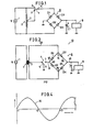
- FIG. 2 is an electric circuit diagram showing in simplified form a power transfer circuit in accordance with the disclosure of DE-A-2007959.
- a power circuit 10 includes a power transformer 2 having a center tap 3 provided at the intermediate portion of secondary winding thereof, a full-wave rectifier circuit 8 in the form of a bridge circuit formed by rectifying diodes D1 to D4 and switching means 4 for grounding the center tap 3 or one output terminal of the full-wave rectifier circuit 8.
- a common terminal 5 of the switching means 4 is grounded at a common potential, while one terminal 6 thereof is connected to the center tap 3 of the power transformer 2 and the other terminal 7 is connected to the said one output terminal of the full-wave rectifier circuit 8 through a line 11.
- the line 11 is connected to anodes of the rectifying diodes D1 and D2 respectively through branch lines 12 and 13.
- the cathode of the rectifying diode D1 is connected to the anode of the rectifying diode D3 through a line 14.
- the cathode of the rectifying diode D2 is connected to the anode of the diode D4 through a line 15.
- the cathodes of the rectifying diodes D3 and D4 are connected to a line 18 through lines 16 and 17 respectively.
- One terminal of the secondary winding of the power transformer 2 is connected to the aforementioned line 14 through a line 19 while the other terminal of the secondary winding is connected to the aforementioned line 15 through a line 110.
- the power circuit 10 in the above described structure is connected through the line 18 to one terminal of a load 9, the other terminal of which is grounded at the common potential.
- the line 18 is connected to an electrolytic capacitor C1, which is grounded at the common potential.
- Figs. 3A and 3B are diagrams for illustrating operation of the circuit as shown in Fig. 2, and Fig. 4 is a waveform diagram of the voltage inputted in the power transformer 2.
- the circuit as shown in Fig. 2 may be regarded equivalent to that shown in Fig. 3A when the common terminal 5 of the switching means 4 is connected to its one terminal 6, since no current flows to the diodes D1 and D2 in this case.
- An AC voltage V having the waveform as shown in Fig. 4 is supplied to the primary winding side of the power transformer 2.
- the current flows in the primary winding side in an arrow A direction while the current flows in the secondary winding side in directions along arrows B, C and D.
- the current flows in the primary winding side in an arrow E direction.
- the current flows in the secondary winding side in directions along arrows F, G and D.
- the power circuit 10 is equivalent to the circuit as shown in Fig. 3B since no current flows to the center tap 3.
- a voltage V having such a waveform as shown in Fig. 4 is applied to the primary side of the power transformer 2.
- the current flows in an arrow A direction in Fig. 3B.
- the current flows in the directions along arrows H, I and J.
- the voltage V2 appearing at the secondary winding side at this time is expressed as follows: Comparing the voltages V1 and V2 obtained in the secondary winding side respectively in Figs. 3A and 3B, the relation between the voltages V1 and V2 is expressed as follows:
- circuit as shown in Fig. 2 can be employed as a double-voltage power transfer circuit by switching the switching means 4.
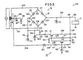
- Fig. 5 is an electric circuit diagram showing the preferred embodiment of the present invention.
- a power circuit 100 mainly includes a power transformer 2, a diode D9 connected between a center tap 3 of the power transformer 2 and the ground, a full-wave rectifier circuit 8 in the form of a bridge circuit, transistors Q1 and Q2 forming a switch operating 14, a thyristor SCR, and Zener diodes ZD1 and ZD2 forming a level discriminator circuit 15.
- the diode D9 and the thyristor SCR form a switching means, the ratio in number of primary winding and secondary winding of the power transformer 2 is selected to be n:2.
- An end of secondary winding 16 of the power transformer 2 is connected to one input end of the full-wave rectifier circuit 8 through a line 120.
- the other end of the secondary winding 16 is connected to the other input end of the full-wave rectifier circuit 8 through a line 121.
- Lines 122 and 123 of the full-wave rectifier circuit 8 are connected to the anodes of diodes D5 and D6, while the cathode of the diode D5 is connected to the anode of a diode D7 through a line 124.
- the cathode of the diode D6 is connected to the anode of a diode D8 through a line 125.
- Respective cathodes of the diodes D7 and D8 are connected to a line 128 respectively through lines 126 and 127.
- the line 128 is connected to a terminal of an electrolytic capacitor C2, the other end of which is grounded at a common potential.
- a junction 100 of the line 128 is connected to the emitter of the transistor Q1 through a line 129.
- the collector of the transistor Q1 is connected to an end of a resistor R3 through a line 130.
- the other end of the resistor R3 is connected to the gate of the thyristor SCR through a line 131.
- the aforementioned lines 122 and 123 of the full-wave rectifier circuit 8 are connected to an end of a resistor R5 through a line 132.
- the other end of the resistor R5 is connected to an end of an electrolytic capacitor C3, the other end of which is grounded at the common potential.
- the aforementioned line 131 is connected to an end of a resistor R4, whose other end is connected to a line 132 through a line 133.
- the anode of the aforementioned thyristor SCR is grounded at the common potential, while the cathode thereof is connected to the aforementioned line 133 through a line 134.
- the junction 101 of the aforementioned line 128 is connected to an end of a resistor R1, the other end of which is connected to an end of the resistor R2 through a line 135.
- the other end of the resistor R2 is grounded at the common potential.
- the line 135 is connected with the base of the transistor Q1.
- a junction 102 of the line 128 is connected to the emitter of the transistor Q2, the collector of which is connected with the line 135 through a line 136.
- the aforementioned line 128 is connected to an end of a resistor R6, the other end of which is connected to an end of a resistor R7 through a line 137.
- the other end of the resistor R7 is connected to the cathode of the Zener diode ZD1 through a line 138.
- the aforementioned line 137 is connected to the base of the transistor Q2 as well as to an end of a resistor R8, the other end of which is connected to the cathode of the Zener diode ZD2.
- the anode of the Zener diode ZD2 is grounded at the common potential.
- the anode of the Zener diode ZD1 is connected through a line 139 to the junction 103 of a line 140 which connects the center tap 3 and the diode D9.
- An end portion of the line 140 is the center tap 3 of the secondary winding 16 of the power transformer 2, and the other end of the line 140 is connected to the cathode of the diode D9, whose anode is grounded at the common potential.
- An intermediate portion between the junction 103 of the line 140 and the diode D9 is connected to an end of an electrolytic capacitor C4, whose other end is grounded at the common potential.
- the junction 105 of the line 128 is connected through a line 142 to an end of a load 17 which other end is grounded at the common potential, so that a voltage E o is applied to the load 17.
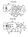
- Figs. 6A and 6B are diagrams for illustrating operation of the circuit as shown in Fig. 5, and Figs. 7 and 8 are diagrams for illustrating changes in voltages at the load 17 and the junction 103 as shown in Fig. 5.
- resistance values of the resistors R1 and R2 are so selected that the transistor Q1 enters an ON state when the transistor Q2 is in an OFF state.
- the current flows to the gate side of the thyristor SCR through the line 129, the transistor Q1 and the resistor R3, whereby the thyristor SCR is made conductive. Therefore, the junction 99 of the full-wave rectifier circuit 8 is grounded at the common potential through the thyristor SCR.
- the power circuit 100 as shown in Fig. 5 is basically equivalent to the circuit as shown in Fig. 6A.
- the transistor Q2 When the transistor Q2 enters an ON state, the voltages at the line 128 and the base of the transistor Q1 reach the same level, whereby the transistor Q1 enters an OFF state. As the result, the current flowing to the gate of the thyristor SCR and the voltage between the anode and the cathode of the thyristor SCR are both eliminated, whereby the thyristor SCR enters an OFF state. As the result, no current flows to the junction 99 of the full-wave rectifier circuit 8. At this time, the junction 103 of the line 140 is at a minus potential as hereinafter described, whereby the current flows to the line 140 through the diode D9. Therefore, the power circuit 100 is basically equivalent to the circuit as shown in Fig. 6B. At this time, the relation between the voltage E 2 appearing at the secondary side of the power transformer 2 and the voltage E1 in Fig. 6A is: Therefore, this circuit 100 implements a power circuit which can be applied to both a single and double voltages.
- the AC voltage V1 in the primary winding side of the power transformer 2 is gradually increased, e.g., from around 80 V.
- the transistor Q2 is in an OFF state while the transistor Q1 and the thyristor SCR are in ON states. Therefore, the power circuit 100 as shown in Fig. 5 is equivalent to the circuit as shown in Fig. 6A.
- the power circuit 100 as shown in Fig. 5 is equivalent to the circuit as shown in Fig. 6B.
- the voltage E 2 appearing at the secondary winding 16 side of the power transformer 2 is as follows, when compared with the voltage E 1 appearing at the secondary winding 16 side in Fig. 6A: Therefore, the voltage E 02 appearing at the load 17 in Fig. 6B is expressed, when compared with the voltage E 01 appearing at the load 17 in Fig. 6A, as follows: Therefore, the voltage at the base of the transistor Q2 is also stepped down and the transistor Q2 inevitably enters an OFF state under such circumstances.
- the current flows to the center tap 3 and the line 140 provided in the secondary winding 16 side of the power transformer 2 through the diode D5, and hence the common potential of the anode of the diode D5 must be higher than the potential at the junction 103. Therefore, the potential at the junction 103 is changed as shown by arrows 22 and 23 in a line 21 in Fig. 8 to be lower than the common potential by the saturation voltage of 0.6 V of the diode D5.
- the potential at the junction 102 is -0.6 V, so that the Zener diode ZD1 is made conductive and a low voltage is applied to the base of the transistor Q2 thereby to retain the transistor Q2 in an ON state.
- the input voltage in the primary winding side of the power transformer 2 is gradually stepped down, e.g., from around 260 V.
- the transistor Q2 is in an ON state while the transistor Q1 and the thyristor SCR are in OFF states.
- the Zener diodes ZD1 and ZD2 are in ON states. Therefore, the power circuit 100 in Fig. 5 is equivalent to the circuit as shown in Fig. 6B.
- the Zener diode ZD1 When the voltage E o at the load 17 is lower than the Zener diode ZD1, i.e., when Eo:-S E 02 in Fig. 7, the Zener diode ZD1 enters an OFF state. Therefore, the transistor Q2 enters an OFF state, whereby the circuit for short-circuiting the base of the transistor Q1 and the line 128 through the transistor Q2 is cut off. The base voltage of the transistor Q2 is stepped down so that the transistor Q1 enters an ON state, whereby the current flows to the gate side of the thyristor SCR, which in turn enters an ON state.
- the output from the full-wave rectifier circuit 8 is discriminated by comparison with the predetermined value set by the Zener diodes ZD1 and ZD2.
- the transistors Q1 and Q2 and the thyristor SCR enter ON/OFF states respectively.
- the output from the full-wave rectifier circuit 8 can be automatically switched between the single voltage and the double voltage in response to the input voltage level.
- Such a power circuit 100 Since no mechanical switching means is required in such a power circuit 100, the circuit is prevented from errors in operation caused by mechanical damage or the like in the portion of the switching means. Further, such a power circuit 100 requires no large-sized transformer, whereby the product to which the power circuit 100 is applied, e.g., a television receiver can be miniaturized to be in lightweight structure.
Landscapes
- Engineering & Computer Science (AREA)
- Power Engineering (AREA)
- Dc-Dc Converters (AREA)
- Rectifiers (AREA)
Claims (4)
gekennzeichnet durch Schaltsteuermittel mit:
Applications Claiming Priority (4)
| Application Number | Priority Date | Filing Date | Title |
|---|---|---|---|
| JP88396/84U | 1984-06-14 | ||
| JP1984088396U JPS617289U (ja) | 1984-06-14 | 1984-06-14 | 電源回路 |
| JP141405/84U | 1984-09-17 | ||
| JP14140584U JPS6155493U (de) | 1984-09-17 | 1984-09-17 |
Publications (2)
| Publication Number | Publication Date |
|---|---|
| EP0168183A1 EP0168183A1 (de) | 1986-01-15 |
| EP0168183B1 true EP0168183B1 (de) | 1989-03-08 |
Family
ID=26429784
Family Applications (1)
| Application Number | Title | Priority Date | Filing Date |
|---|---|---|---|
| EP85304281A Expired EP0168183B1 (de) | 1984-06-14 | 1985-06-14 | Leistungsübertragungskreis |
Country Status (8)
| Country | Link |
|---|---|
| US (1) | US4675801A (de) |
| EP (1) | EP0168183B1 (de) |
| AU (1) | AU578389B2 (de) |
| BR (1) | BR8502836A (de) |
| CA (1) | CA1236521A (de) |
| DE (1) | DE3568675D1 (de) |
| ES (1) | ES8608247A1 (de) |
| PH (1) | PH22305A (de) |
Families Citing this family (11)
| Publication number | Priority date | Publication date | Assignee | Title |
|---|---|---|---|---|
| JPS62166780A (ja) * | 1986-01-17 | 1987-07-23 | Sharp Corp | 交流入力フリ−電源 |
| DE3612147A1 (de) * | 1986-04-10 | 1987-10-15 | Philips Patentverwaltung | Schaltungsanordnung zur erzeugung einer gleichspannung aus einer sinusfoermigen eingangsspannung |
| JPS63311419A (ja) * | 1987-06-13 | 1988-12-20 | Mitsuoka Denki Seisakusho:Kk | 直流電源装置 |
| US4780805A (en) * | 1987-07-21 | 1988-10-25 | Ncr Corporation | Low/high input voltage power supply |
| US4864488A (en) * | 1988-06-27 | 1989-09-05 | Ncr Corporation | Single level D.C. output voltage power supply |
| JP2886176B2 (ja) * | 1989-03-23 | 1999-04-26 | 三菱電機株式会社 | 埋め込みチャネルの物性特性測定法 |
| US6278266B1 (en) * | 1994-06-17 | 2001-08-21 | Martin S. Glasband | Symmetrical power generator and method of use |
| US5640314A (en) * | 1994-06-17 | 1997-06-17 | Equi-Tech Licensing Corp. | Symmetrical power system |
| WO2000070733A1 (en) * | 1999-05-12 | 2000-11-23 | Medar, Inc. | Method and system for controlling ac current supplied to an inductive load from an ac powerline |
| JP2000350458A (ja) * | 1999-06-03 | 2000-12-15 | Sony Corp | 電源装置 |
| TWI620404B (zh) * | 2015-06-05 | 2018-04-01 | 宸定科技股份有限公司 | 一種可應用於外接式硬碟之電源轉換電路 |
Family Cites Families (4)
| Publication number | Priority date | Publication date | Assignee | Title |
|---|---|---|---|---|
| US2777107A (en) * | 1953-04-01 | 1957-01-08 | Fox Prod Co | Rectifying systems |
| NL294326A (de) * | 1962-06-27 | |||
| BE746136A (fr) * | 1969-02-20 | 1970-07-31 | Ampex | Source d'alimentation electrique |
| US4001668A (en) * | 1973-11-16 | 1977-01-04 | Schick Incorporated | Electric shaver operable from a wide range of supply voltages |
-
1985
- 1985-05-16 AU AU42554/85A patent/AU578389B2/en not_active Expired
- 1985-05-20 US US06/735,757 patent/US4675801A/en not_active Expired - Lifetime
- 1985-05-23 CA CA000482211A patent/CA1236521A/en not_active Expired
- 1985-06-10 PH PH32386A patent/PH22305A/en unknown
- 1985-06-13 ES ES544138A patent/ES8608247A1/es not_active Expired
- 1985-06-13 BR BR8502836A patent/BR8502836A/pt not_active IP Right Cessation
- 1985-06-14 DE DE8585304281T patent/DE3568675D1/de not_active Expired
- 1985-06-14 EP EP85304281A patent/EP0168183B1/de not_active Expired
Also Published As
| Publication number | Publication date |
|---|---|
| PH22305A (en) | 1988-07-22 |
| DE3568675D1 (en) | 1989-04-13 |
| US4675801A (en) | 1987-06-23 |
| AU4255485A (en) | 1985-12-19 |
| AU578389B2 (en) | 1988-10-20 |
| ES8608247A1 (es) | 1986-06-01 |
| EP0168183A1 (de) | 1986-01-15 |
| CA1236521A (en) | 1988-05-10 |
| BR8502836A (pt) | 1986-02-25 |
| ES544138A0 (es) | 1986-06-01 |
Similar Documents
| Publication | Publication Date | Title |
|---|---|---|
| US5144547A (en) | Rectifying circuit with FETs | |
| EP0112119B1 (de) | Gleichrichterbrückenschaltung | |
| EP0168183B1 (de) | Leistungsübertragungskreis | |
| US5118993A (en) | Variable voltage regulator | |
| US4150423A (en) | Transformer coupled pass element | |
| US3049623A (en) | Auxiliary power supply | |
| HK95191A (en) | Two-mode switching power supply | |
| US4560841A (en) | Telephone station which is main or remotely supplied | |
| US6462924B1 (en) | Power supply apparatus comprising a voltage detection circuit and method for using same | |
| US3720868A (en) | Multiple input voltage source power supply | |
| US4947313A (en) | Direct current power supply | |
| US3085234A (en) | Magnetostatic relay | |
| US4314327A (en) | Transistor drive control for a multiple input D.C. to D.C. converter | |
| EP0345192A2 (de) | Stromversorgung, die von veränderlichen Wechselstromeingangsspannungen konstante Gleichstromausgangsspannungen liefert | |
| EP0902530A2 (de) | Spannungswandler | |
| US4308576A (en) | Overload protection for a voltage conversion circuit | |
| US3939394A (en) | Constant voltage circuit | |
| US3772583A (en) | Power supply circuit | |
| JPH11136939A (ja) | スイッチング電源 | |
| KR900007132Y1 (ko) | 전원 절환 회로 | |
| JPH0424789Y2 (de) | ||
| JPS58212370A (ja) | 電源回路 | |
| US4641230A (en) | Pulse absorption circuit for power source circuit | |
| US4075685A (en) | Emitter follower voltage controlled power supply | |
| JPH0248889Y2 (de) |
Legal Events
| Date | Code | Title | Description |
|---|---|---|---|
| PUAI | Public reference made under article 153(3) epc to a published international application that has entered the european phase |
Free format text: ORIGINAL CODE: 0009012 |
|
| AK | Designated contracting states |
Designated state(s): DE FR GB |
|
| 17P | Request for examination filed |
Effective date: 19860217 |
|
| 17Q | First examination report despatched |
Effective date: 19861117 |
|
| GRAA | (expected) grant |
Free format text: ORIGINAL CODE: 0009210 |
|
| AK | Designated contracting states |
Kind code of ref document: B1 Designated state(s): DE FR GB |
|
| REF | Corresponds to: |
Ref document number: 3568675 Country of ref document: DE Date of ref document: 19890413 |
|
| ET | Fr: translation filed | ||
| PLBE | No opposition filed within time limit |
Free format text: ORIGINAL CODE: 0009261 |
|
| STAA | Information on the status of an ep patent application or granted ep patent |
Free format text: STATUS: NO OPPOSITION FILED WITHIN TIME LIMIT |
|
| 26N | No opposition filed | ||
| REG | Reference to a national code |
Ref country code: GB Ref legal event code: IF02 |
|
| PGFP | Annual fee paid to national office [announced via postgrant information from national office to epo] |
Ref country code: FR Payment date: 20040608 Year of fee payment: 20 |
|
| PGFP | Annual fee paid to national office [announced via postgrant information from national office to epo] |
Ref country code: GB Payment date: 20040609 Year of fee payment: 20 |
|
| PGFP | Annual fee paid to national office [announced via postgrant information from national office to epo] |
Ref country code: DE Payment date: 20040624 Year of fee payment: 20 |
|
| PG25 | Lapsed in a contracting state [announced via postgrant information from national office to epo] |
Ref country code: GB Free format text: LAPSE BECAUSE OF EXPIRATION OF PROTECTION Effective date: 20050613 |
|
| REG | Reference to a national code |
Ref country code: GB Ref legal event code: PE20 |