EP0169018A2 - Computerspeicheranordnung - Google Patents
Computerspeicheranordnung Download PDFInfo
- Publication number
- EP0169018A2 EP0169018A2 EP85304873A EP85304873A EP0169018A2 EP 0169018 A2 EP0169018 A2 EP 0169018A2 EP 85304873 A EP85304873 A EP 85304873A EP 85304873 A EP85304873 A EP 85304873A EP 0169018 A2 EP0169018 A2 EP 0169018A2
- Authority
- EP
- European Patent Office
- Prior art keywords
- memory
- user processor
- memory system
- block
- blocks
- Prior art date
- Legal status (The legal status is an assumption and is not a legal conclusion. Google has not performed a legal analysis and makes no representation as to the accuracy of the status listed.)
- Withdrawn
Links
Images


Classifications
-
- G—PHYSICS
- G06—COMPUTING OR CALCULATING; COUNTING
- G06F—ELECTRIC DIGITAL DATA PROCESSING
- G06F12/00—Accessing, addressing or allocating within memory systems or architectures
- G06F12/02—Addressing or allocation; Relocation
- G06F12/0223—User address space allocation, e.g. contiguous or non contiguous base addressing
- G06F12/023—Free address space management
Definitions
- This invention relates to improvements in memory systems, and more particularly to improvements in a memory system of the type which enable automatic memory operations independently of a user processor with which it is associated.
- a garbage collected memory is one in which usable memory is automatically reclaimed, and the memory may be reorganized from time to time to efficiently utilize the space of the memory, as needed.
- a background survey of garbage collection techniques and related background materials is presented by Cohen, J. "Garbage Collection of Linked Data Structures", Computing Surveys, Vol. 13, No. 3, September, 1981, pp. 341-367, and also by P. Bishop, “Garbage Collection in a Very Large Address Space", Massachusetts Institute of Technology, Working Paper 111, September, 1975.
- Thatte et al describes a computer system having an associated CPU.
- the system enables automatic memory operations, in general, and the present invention discloses a particular implementation of the general system in which the user CPU can be provided entirely separate from the memory system.
- an object of the invention to provide a memory system which enables automatic memory operations independently of the user processor with which it is associated.
- MMU memory management unit
- the memory system in accordance with a broad aspect of the invention, presents a memory system which is characterized in that it responds to conditions, commands or instructions from a user CPU to allocate memory blocks and allows the user CPU to execute read, write, move and EQ test instructions with regard to the allocated memory blocks.
- the memory system operation is based upon the use of binding registers which interface the user CPU to the memory, and which enables the memory to be seen by the user CPU as a block oriented memory, and which permits the memory management unit to control memory overhead functions independently and practically invisibly from the user CPU.
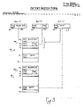
- FIG. 5 is a box diagram of a generalized hardware implementation of the memory system, in accordance with the invention.
- the memory system 10 of the invention includes a memory management unit 11 and physical memory 12, associated with a user CPU 20 (sometimes referred to as the user processor).
- a user CPU 20 sometimes referred to as the user processor.
- MMU memory management unit
- the responsibilities of the user CPU 20 and the memory management unit (MMU) 11 advanced herein are separate. That is, the CPU 20 has no memory management responsibilities, and the MMU 11 can freely move data within the memory. Moreover, the CPU 20 can not accidentally or intentionally destroy or change the structural information of the memory which is necessary to maintain the organizational integrity of the memory.
- the user CPU 20 can be practically any type or kind compatible with the memory system 10.
- the memory system 10 has the appearance to the user CPU 20 of being block oriented. With reference now to Figure 2, despite the actual or hardware configuration of the memory system 10, it has an apparent logical memory organization (10) as seen by the user CPU 20, as indicated by the reference numeral (10) and its associated dotted arrow.
- the logical memory organization (10) is referred to herein as a "logical address space", and, as will become apparent, is distinguished from a "virtual address space” which is a memory representation or abstraction as seen by the memory management unit, below described, and from a physical memory, which is the actual physical memory elements of the memory system.
- the logical memory system 10 has a binding register unit 15, described below in detail with reference to Figure 3, which serves as a window or portal into and out of the logical memory system (10).
- the binding register unit 15 is a real part of the memory system 10, and is responsible for converting the block oriented view or logical address space seen by the user CPU into the virtual address space in which the memory management actually takes place.
- the philosophy of the binding register unit 15 is based upon the notion that at any instant, the user processor 20 can directly address only a limited number of blocks; more specifically, the user processor can directly address those blocks whose pointers are contained in a set of binding registers within the binding register unit 15.
- the user CPU 20 typically uses the binding register unit 15 in two modes of operation.
- the binding register 15 may be loaded with a block identifier (i.e. a pointer to a block) in order to establish the addressability of a particular block in memory.
- a block identifier i.e. a pointer to a block
- binding is used to emphasize the association of the register with the block.
- pointer is used to denote a value or data which specifies an address of a particular block of memory.
- the other primary mode of operation of the binding register 15 is as a base for referencing some value within a previously bound block.
- the MMU in response to a CPU request for the data in a specified relative block location, the MMU develops an address for the particular value to be found or contained within the block by adding an index count to the contents of the block address field contained in the binding register. It will be appreciated that it is necessary to verify that the index is a valid one for the particular block, for example, that the index does not specify the fourth word of a two word block.
- the binding register unit supports this type of addressing as a relative index to a register name which is currently bound to a block. It therefore provides complete checking to see that the index is valid before permitting the reference.
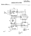
- the binding register unit 15 includes a number or set of individual binding registers 21, 22, ...30, each of which being addressable and manipulatable by the user CPU 20.
- the manner by which the user CPU addresses the binding registers can be, for example, merely by specifying a particular binding register, such as "register 1", "register 5", and so on.
- the binding register unit 15 may have as many binding registers as needed for the particular application of the memory management unit under consideration.
- each of the blocks which are established includes a header portion 40h and 45h, at least a portion of which is reproduced into one of the binding registers 20-30 of the binding register unit 15.
- the header of each respective block may contain, among other things, block identifying data, block length data, block type data, flags, and the like.
- each block 40 and 45 are data words 40d and 45d, respectively.
- the data words 40d and 45 d are displaced from the respective headers of the blocks 40 and 45 by a number of address locations.
- the number of address locations depends on many factors, including the specification of a particular address displacement by the user CPU. More particularly, the user CPU can write data into the block 40 at location 40d by specifying a displacement from the header, contained, for instance, in register 21 of the binding register unit 15.
- the manner by which the user CPU specifies the desired block location is by specifying the particular binding register to which the block is bound (for instance, "register i") and the displacement within the bound block (for instance. "j").
- the specified value can then be returned directly to the user CPU as data, or can be written into the binding register unit in (the same or different) specified binding register.
- the user CPU 20 may issue a command to the memory system (10) to create a block, for instance the block illustrated which is denoted by the reference numeral 40, of some specified length.
- the CPU issues a direction to the MMU to place a pointer to the block 40 in a CPU directed target binding register, such as register 21.
- the CPU 20 might issue a command to write data into the block 40 by specifying a displacement "j" from the address of the header pointed to by the pointer in binding register 21.
- the CPU 10 only specifies the particular binding register (21) containing the pointer and the displacement "j", not the address of the block 40.
- Each binding register has two parts, denoted Part "a" and Part "b". Each of the parts a-b contains certain block identifying information, as below described in detail.
- a particular block location or address is referenced by the user CPU by a relative index.
- the particular location referenced is a cell denoted by Pc in a previously bound referencing block 45 at a displacement "i" from the header 45h.
- This cell, Pc has two segments, the first segment 64 for a memory management unit tag, and the second segment 71 for either a pointer to the header of a referenced block or for data. (In either case, the contents of segment 71 appear as "data" to an observer.)
- the MMU tag 64 indicates whether or not the "data” is in fact a pointer.
- the "data" word in the segment 71 of the Pc cell is or contains the pointer reference to the header information 40h of the next subsequent block (block 40) to be bound to the binding register unit.
- the information in the first and second registers of the header 40h is then copied to registers Part "a" and Part "b” in the manner described below, thereby completing the binding process. Additional information not of interest herein may also be contained in the header portion 40h.
- Part "b" of the binding register also has two segments of interest.
- the first segment 63 is for a memory management unit tag 63 and a second segment 69 is for certain flags.
- the flags in the flag portion 70 of register Part "b" of the binding register may contain numerous flags, examples of which are “lock”, "bound", and so on.
- a lock flag may be used, for example, in the establishment or moving of the block during which time any addressing of the block by other than the memory management unit is prohibited.
- a bound flag may be, for example, used to indicate that the block is bound to a binding register.
- the hardware for realizing a binding register unit 15 in accordance with the invention includes a CPU interface 80 for connection between the user CPU 20 ( Figure 1) and the binding register unit 15, on the one hand, and a processor interface 81 for connection between a memory management unit controlling processor ( Figure 5, described below) and the binding register unit 15.
- the binding register unit 15 includes a binding register file 83 for containing individual binding registers into which information is written, as above described.
- the binding register file 83 is connected directly to the CPU interface 80.
- the binding register file 83 is connected to the processor interface 81 by a data path controlling circuit 84.
- an instruction decoder 90 is provided, with connection to the CPU interface 80 to receive instructions from the user processor, and to operate to decode_the particular instructions issued by the user CPU.
- the output from the instruction decoder 90 is directed to a sequencer 92 and a microcode generator or control ROM/RAM 93.
- the microcode generator or control ROM/RAM 93 in conjunction with the MMU processor, controls the operation of the binding register file 83 and the data path selection circuit 84.
- the circuitry for the binding register unit 15 can be fabricated in standard TTL or MSI circuitry or on a custom LSI or VLSI chip using well known techniques.
- the operation of the binding register 15 to effect the memory architecture described is under the control of the microcode control program in the microcode ROM/RAM 93.
- the design of the microcode will depend upon such factors as the type of memory processor employed (described below), the type of hardware for construction of the memory system, and so on.
- a LISP program which can be run on a standard LISP machine to simulate the operation of the memory system of the invention, including the binding register unit, is shown in Appendix A attached hereto. It will be understood that various other forms of implementation of the memory system can be equally advantageously employed.
- the hardware for realizing the memory management unit 11 in conjunction with the physical memory 12 to form the memory system 10 of the invention is quite general, and is shown in Figure 5.
- the memory system 10 includes a binding register unit 15, as above described, connected to the user CPU 20 (see Figure 1).
- command, binding register, index, data, control and status lines are provided to the user CPU 20 from the binding register unit 15 as above described.
- the operation of the memory management unit 11 is controlled by a processor 100, to which command, virtual address, control and data lines are provided for connection to the binding register unit 15, as shown.
- various memory interfacing apparatuses can be provided for control by the processor 100.
- a main memory 102 which may include, for instance, a hard wired physical memory of semiconductors, bubble domain cells, or any other memory elements known in the art.
- the main memory 102 is connected to the binding register unit 15 by a page table unit 104.
- the data flow between the binding register unit 15 and physical memory 102 is controlled through the page table unit 104 by the processor 100, or the binding register unit 15, having command, virtual address, control and data lines connected between the binding register unit 15, the processor 100 and page table unit 104.
- a disk unit 106 may be provided as a form of memory with which the memory management unit 11 in accordance with the invention may be used.
- the disk unit 106 can be of any magnetic disk, optical, or other well known disk memory, as known in the art.
- the disk unit 106 is controlled by a disk controller 108, again controlled by the processor 100 by control, data, and command lines, and interfaces with the binding register unit 15 and page table unit 104 by data, control and physical address lines, as shown, for data transfers.
- main memory 102 and disk unit 106 are shown, it is not intended that the invention be limited in any way to such memory types, as it will be apparent to those skilled in the art that other memory types and configurations can be equally advantageously employed in practicing the invention.
- one or more flags are provided in the block header. At least one of the flags serves as a lock so that, when set, no changes can be made by the user CPU to the block. This is useful, for example, when the block is being copied, moved, rearranged, and the like, for instance during garbage collection or other action being performed by the memory management unit.
- Another flag which may be employed is to determine whether the block is bound or not. Thus, when the memory system wishes to move or modify a block, it must be able to determine if the block is currently bound to a binding register.
- the block size indication in register portion 68 of Part "a" of the binding register is necessary to determine whether an index exceeds the valid length of the block.
- the MMU tags in segments 62, 63 and 64 are associated with both the header and the data portions of the block.
- the tags required by the memory management unit are enforced by the binding register unit so that the user processor is prevented from writing a tag or "pointer" and also to verify that a cell actually contains a pointer before attempting to bind a particular block.
- the tags cannot be arbitrarily set by the user processor.
- the memory management unit must continually verify that the user processor is not attempting to set prohibited tags, that is, pointers, headers, forwards, and so on.
- each pointer carries an MMU tag indicating that the data represents a pointer, the pointers within the blocks may not be modified by the user processor.
- the user processor can, however, over-write the pointer with data, which would result in the destruction of the pointer reference, but is prohibited from direct alteration or modification of the pointer.
- the memory system is addressable or accessible in the logical address space by a number of predetermined commands.
- the commands which can be used are (1) a command to allocate block space; (2) a command to copy a pointer from one binding register or indexed block cell to another binding register or block cell within the logical address space; (3) a command to perform an "EQ test" which tests two binding registers or block cells in the logical address space to determine whether they both (a) contain pointers which refer to the same block or (b) contain the same data; (4) a command to read an indexed location in a specified block; and (5) a command to write user processor generated data into an indexed location in a specified block.
- the allocate command, copy instruction and the "EQ Test" serve to enable the user processor to determine the configuration of the memory system and to arrange the memory system to any desired configuration.
- the read and write commands allow the processor to interact with the memory. Even so, it should be noted that the user processor is not permitted to write pointers into the logical address space.
- other commands can be equally advantageously employed, as will be apparent to those skilled in the art, the above enumerated commands are presently considered to be minimally required of the memory system of the invention; that is, it is considered that the five commands enable the operation of the memory system, and distinguish it from memory systems of the prior art.
- the memory system 10 is first associated with a user processor 20.
- the user processor 20 can be of any kind or type, so long as it is able to communicate with the binding register unit 15.
- the restriction is merely a hardware compatibility restriction, it has nothing to do with the operation of the memory, its hierarchy, its organization, etc.
- the user processor When the user processor wishes to write into memory, it first issues a block allocate command to the memory management system 10. As a part of the block allocate command, the user processor specifies the size of the block desired and a binding register to which the block to be allocated or created is bound. The memory system then creates the requested block. The user processor 20 may then issue a write command directed to the specified binding register, and stating a relative block location at which the processor desires that data be written. Thereafter, if it is desired to read the data previously written, the processor 20 issues a read statement directed to the binding register to which the block is bound at that time specifying the offset at which the data was previously written. The memory management system then delivers to the user processor the previously written data.
- One aspect of the operation of the memory system 10 includes the formulation and operation of the pointer system within the allocated blocks.
- a pointer may be established at a relative address in the referencing block to the referenced block.
- the pointer would be established by the memory management unit 11, not by the user processor, and would be located at an indexed relative location in the referencing block.
- the user processor may request the MMU to establish a pointer, but the MMU itself creates and manages the pointers.
- the user processor can issue an EQ test command to the memory system 10 to determine whether two relative locations in a particular block or in two blocks contain pointers to the same block.
- the EQ test can also be used to determine whether two particular relative locations of the same or different block contain the same data). It should be noted that although the relative locations of the allocated blocks can be read directly by the user processor, if the relative locations contain pointers to other blocks, the pointers read may not necessarily be the same even though they may be declared equal upon execution by the EQ test. For example, a block may contain an invisible pointer which would result in an apparent different reference. For instance, if a pointer of say block A points to block B, and a pointer of block C points to block D which in turn points to block B, the pointers of blocks A and C would point to the same block and would therefore be declared equal by the EQ test, but would not appear to be equal if viewed by the user processor as data.
- garbage collection can be implemented automatically, without a requirement that the ongoing processing steps of the user processor be halted during the garbage collection process.
- the garbage collection techniques can be generally any techniques which have been heretofore used, examples of which are shown in an article by G. Baker, Jr., "List Processing in Real Time on a Serial Computer", Communications of the ACM, Vol. 21, No. 4. April. 1978. Inasmuch as the garbage collection within the memory unit 10 is invisible to the user CPU, and independent of it, the garbage collection techniques used can, in fact, efficiently be compacting garbage collection techniques, enabling even more efficient use of the physical memory of the memory management unit 10.
- each block which is allocated is known and cannot be exceeded in use.
- the memory is protected from accidental or intentional destruction by the user, for instance, by an attempt to write data or other matter into one block at an index beyond the length of the block.
Landscapes
- Engineering & Computer Science (AREA)
- Theoretical Computer Science (AREA)
- Physics & Mathematics (AREA)
- General Engineering & Computer Science (AREA)
- General Physics & Mathematics (AREA)
- Memory System (AREA)
- Techniques For Improving Reliability Of Storages (AREA)
Applications Claiming Priority (2)
| Application Number | Priority Date | Filing Date | Title |
|---|---|---|---|
| US630476 | 1975-11-10 | ||
| US06/630,476 US4989137A (en) | 1984-07-12 | 1984-07-12 | Computer memory system |
Publications (2)
| Publication Number | Publication Date |
|---|---|
| EP0169018A2 true EP0169018A2 (de) | 1986-01-22 |
| EP0169018A3 EP0169018A3 (de) | 1989-09-13 |
Family
ID=24527332
Family Applications (1)
| Application Number | Title | Priority Date | Filing Date |
|---|---|---|---|
| EP85304873A Withdrawn EP0169018A3 (de) | 1984-07-12 | 1985-07-09 | Computerspeicheranordnung |
Country Status (3)
| Country | Link |
|---|---|
| US (1) | US4989137A (de) |
| EP (1) | EP0169018A3 (de) |
| JP (1) | JPS61112257A (de) |
Cited By (1)
| Publication number | Priority date | Publication date | Assignee | Title |
|---|---|---|---|---|
| FR2679671A1 (fr) * | 1991-07-25 | 1993-01-29 | Sogitec Ind | Processeur de structures complexes. |
Families Citing this family (22)
| Publication number | Priority date | Publication date | Assignee | Title |
|---|---|---|---|---|
| JP2545789B2 (ja) * | 1986-04-14 | 1996-10-23 | 株式会社日立製作所 | 情報処理装置 |
| US5384900A (en) * | 1988-03-14 | 1995-01-24 | Canon Kabushiki Kaisha | Method of managing an image memory by a process independent of an image processing process |
| JPH0244444A (ja) * | 1988-08-05 | 1990-02-14 | Nec Corp | メモリ管理方式 |
| US5189733A (en) * | 1989-08-22 | 1993-02-23 | Borland International, Inc. | Application program memory management system |
| EP0416767A3 (en) * | 1989-09-08 | 1992-04-29 | Digital Equipment Corporation | Position independent code location system |
| US5414826A (en) * | 1990-01-31 | 1995-05-09 | Hewlett-Packard Company | System and method for memory management in microcomputer |
| US5410671A (en) * | 1990-05-01 | 1995-04-25 | Cyrix Corporation | Data compression/decompression processor |
| JPH0418638A (ja) * | 1990-05-11 | 1992-01-22 | Fujitsu Ltd | 静的メモリ割当て処理方法 |
| US5355483A (en) * | 1991-07-18 | 1994-10-11 | Next Computers | Asynchronous garbage collection |
| US5809551A (en) * | 1991-08-23 | 1998-09-15 | International Business Machines Corporation | Pending page release |
| US5742793A (en) * | 1991-12-18 | 1998-04-21 | Intel Corporation | Method and apparatus for dynamic memory management by association of free memory blocks using a binary tree organized in an address and size dependent manner |
| JPH06511582A (ja) * | 1992-07-24 | 1994-12-22 | マイクロソフト コーポレイション | メモリを割り当てそして解放するコンピュータ方法及びシステム |
| US6131150A (en) * | 1993-10-05 | 2000-10-10 | Digital Equipment Corporation | Scaled memory allocation system |
| US5611043A (en) * | 1994-03-18 | 1997-03-11 | Borland International, Inc. | Debugger system and method for controlling child processes |
| US6745213B2 (en) * | 2001-11-21 | 2004-06-01 | Sun Microsystems, Inc. | Method and apparatus to facilitate testing of garbage collection implementations |
| US8042189B2 (en) | 2002-03-20 | 2011-10-18 | Research In Motion Limited | System and method to force a mobile device into a secure state |
| JP2005521133A (ja) | 2002-03-20 | 2005-07-14 | リサーチ イン モーション リミテッド | 移動装置における機密保護ガーベージコレクション・システムおよび方法 |
| CN103473181B (zh) | 2007-01-26 | 2017-06-13 | 英特尔公司 | 分级式不可变内容可寻址存储器处理器 |
| US9601199B2 (en) | 2007-01-26 | 2017-03-21 | Intel Corporation | Iterator register for structured memory |
| US8156256B2 (en) * | 2007-04-24 | 2012-04-10 | Samsung Electronics Co., Ltd. | Method for managing logical address and device thereof |
| WO2009085253A1 (en) * | 2007-12-21 | 2009-07-09 | Hicamp Systems | Hierarchical block-identified data communication for unified handling of structured data and data compression |
| US10089235B1 (en) | 2017-07-28 | 2018-10-02 | Citrix Systems, Inc. | Dynamic trim processing with disk caching |
Family Cites Families (5)
| Publication number | Priority date | Publication date | Assignee | Title |
|---|---|---|---|---|
| US4149240A (en) * | 1974-03-29 | 1979-04-10 | Massachusetts Institute Of Technology | Data processing apparatus for highly parallel execution of data structure operations |
| US4016545A (en) * | 1975-07-31 | 1977-04-05 | Harris Corporation | Plural memory controller apparatus |
| DE2641722C3 (de) * | 1976-09-16 | 1981-10-08 | Siemens AG, 1000 Berlin und 8000 München | Hierarchisch geordnetes Speichersystem für eine datenverarbeitende Anlage mit virtueller Adressierung |
| US4398248A (en) * | 1980-10-20 | 1983-08-09 | Mcdonnell Douglas Corporation | Adaptive WSI/MNOS solid state memory system |
| JPS5740790A (en) * | 1980-08-25 | 1982-03-06 | Fujitsu Ltd | Storage control system |
-
1984
- 1984-07-12 US US06/630,476 patent/US4989137A/en not_active Expired - Fee Related
-
1985
- 1985-07-09 EP EP85304873A patent/EP0169018A3/de not_active Withdrawn
- 1985-07-12 JP JP60153911A patent/JPS61112257A/ja active Pending
Cited By (1)
| Publication number | Priority date | Publication date | Assignee | Title |
|---|---|---|---|---|
| FR2679671A1 (fr) * | 1991-07-25 | 1993-01-29 | Sogitec Ind | Processeur de structures complexes. |
Also Published As
| Publication number | Publication date |
|---|---|
| EP0169018A3 (de) | 1989-09-13 |
| US4989137A (en) | 1991-01-29 |
| JPS61112257A (ja) | 1986-05-30 |
Similar Documents
| Publication | Publication Date | Title |
|---|---|---|
| US4757438A (en) | Computer system enabling automatic memory management operations | |
| US4989137A (en) | Computer memory system | |
| US4775932A (en) | Computer memory system with parallel garbage collection independent from an associated user processor | |
| US4742447A (en) | Method to control I/O accesses in a multi-tasking virtual memory virtual machine type data processing system | |
| US4761737A (en) | Method to automatically increase the segment size of unix files in a page segmented virtual memory data processing system | |
| US4853842A (en) | Computer memory system having persistent objects | |
| US6125434A (en) | Dynamic memory reclamation without compiler or linker assistance | |
| US6125430A (en) | Virtual memory allocation in a virtual address space having an inaccessible gap | |
| EP0238158B1 (de) | Anteilige Nutzung von Kopie-beim-Schreiben-Segmenten in einer Datenverarbeitungsanlage mit virtuellen Maschinen und virtuellem Speicher | |
| US6112285A (en) | Method, system and computer program product for virtual memory support for managing translation look aside buffers with multiple page size support | |
| US5088026A (en) | Method for managing a data cache using virtual external storage addresses as arguments | |
| US5390310A (en) | Memory management unit having cross-domain control | |
| Lampson et al. | An open operating system for a single-user machine | |
| US5539899A (en) | System and method for handling a segmented program in a memory for a multitasking data processing system utilizing paged virtual storage | |
| US5175830A (en) | Method for executing overlays in an expanded memory data processing system | |
| US8473722B2 (en) | Processor architecture for exact pointer identification | |
| US5062039A (en) | Sharing of workspaces in interactive processing using workspace name tables for linking of workspaces | |
| US5875487A (en) | System and method for providing efficient shared memory in a virtual memory system | |
| JP3629507B2 (ja) | コンピュータ・システム内で共用仮想セグメント識別を使用して共用メモリを提供するシステムおよび方法 | |
| US5388244A (en) | Controls for initial diversion of page-frame logical content as part of dynamic virtual-to-real translation of a virtual page address | |
| US7293207B2 (en) | Method for testing memory in a computer system utilizing a CPU with either 32-bit or 36-bit memory addressing | |
| US6279148B1 (en) | Method and apparatus for supporting efficient programming in dynamic pointer-safe languages | |
| JPH0564817B2 (de) | ||
| Shirriff | An Implementation of Memory Sharing and File Mapping | |
| Hollmann | Page Eviction for Self-Contained Virtual-Memory Objects in the Linux Kernel |
Legal Events
| Date | Code | Title | Description |
|---|---|---|---|
| PUAI | Public reference made under article 153(3) epc to a published international application that has entered the european phase |
Free format text: ORIGINAL CODE: 0009012 |
|
| AK | Designated contracting states |
Designated state(s): DE FR GB |
|
| PUAL | Search report despatched |
Free format text: ORIGINAL CODE: 0009013 |
|
| AK | Designated contracting states |
Kind code of ref document: A3 Designated state(s): DE FR GB |
|
| STAA | Information on the status of an ep patent application or granted ep patent |
Free format text: STATUS: THE APPLICATION IS DEEMED TO BE WITHDRAWN |
|
| 18D | Application deemed to be withdrawn |
Effective date: 19900314 |
|
| RIN1 | Information on inventor provided before grant (corrected) |
Inventor name: KNIGHT, WILLIAM M. JR. Inventor name: LOAFMAN, JERI J. Inventor name: OXLEY, DONALD W. Inventor name: MANUEL, GLENN E. |