EP0169078A2 - Von der Verbindung Nb3Sn hergestellter Supraleiter - Google Patents
Von der Verbindung Nb3Sn hergestellter Supraleiter Download PDFInfo
- Publication number
- EP0169078A2 EP0169078A2 EP85305169A EP85305169A EP0169078A2 EP 0169078 A2 EP0169078 A2 EP 0169078A2 EP 85305169 A EP85305169 A EP 85305169A EP 85305169 A EP85305169 A EP 85305169A EP 0169078 A2 EP0169078 A2 EP 0169078A2
- Authority
- EP
- European Patent Office
- Prior art keywords
- region
- alloy
- compound
- pipe
- superconductor
- Prior art date
- Legal status (The legal status is an assumption and is not a legal conclusion. Google has not performed a legal analysis and makes no representation as to the accuracy of the status listed.)
- Withdrawn
Links
- 239000002887 superconductor Substances 0.000 title claims abstract description 63
- 150000001875 compounds Chemical class 0.000 title claims abstract description 31
- 229910000657 niobium-tin Inorganic materials 0.000 title claims abstract description 28
- 229910045601 alloy Inorganic materials 0.000 claims abstract description 55
- 239000000956 alloy Substances 0.000 claims abstract description 55
- 229910017755 Cu-Sn Inorganic materials 0.000 claims abstract description 53
- 229910017927 Cu—Sn Inorganic materials 0.000 claims abstract description 53
- KUNSUQLRTQLHQQ-UHFFFAOYSA-N copper tin Chemical compound [Cu].[Sn] KUNSUQLRTQLHQQ-UHFFFAOYSA-N 0.000 claims abstract description 53
- 230000004888 barrier function Effects 0.000 claims abstract description 25
- 239000010949 copper Substances 0.000 claims abstract description 21
- LEONUFNNVUYDNQ-UHFFFAOYSA-N vanadium atom Chemical compound [V] LEONUFNNVUYDNQ-UHFFFAOYSA-N 0.000 claims abstract description 19
- 229910052720 vanadium Inorganic materials 0.000 claims abstract description 17
- RYGMFSIKBFXOCR-UHFFFAOYSA-N Copper Chemical compound [Cu] RYGMFSIKBFXOCR-UHFFFAOYSA-N 0.000 claims abstract description 4
- 229910052802 copper Inorganic materials 0.000 claims abstract description 4
- 239000010955 niobium Substances 0.000 claims description 36
- 230000000087 stabilizing effect Effects 0.000 claims description 24
- GUCVJGMIXFAOAE-UHFFFAOYSA-N niobium atom Chemical compound [Nb] GUCVJGMIXFAOAE-UHFFFAOYSA-N 0.000 claims description 4
- 239000000945 filler Substances 0.000 claims description 2
- 239000000463 material Substances 0.000 claims 1
- 238000010438 heat treatment Methods 0.000 abstract description 12
- 229910052734 helium Inorganic materials 0.000 abstract description 6
- 239000001307 helium Substances 0.000 abstract description 6
- SWQJXJOGLNCZEY-UHFFFAOYSA-N helium atom Chemical compound [He] SWQJXJOGLNCZEY-UHFFFAOYSA-N 0.000 abstract description 6
- 239000007788 liquid Substances 0.000 description 4
- 238000000034 method Methods 0.000 description 3
- 229910052758 niobium Inorganic materials 0.000 description 3
- 238000010276 construction Methods 0.000 description 2
- 230000008878 coupling Effects 0.000 description 2
- 238000010168 coupling process Methods 0.000 description 2
- 238000005859 coupling reaction Methods 0.000 description 2
- 238000004519 manufacturing process Methods 0.000 description 2
- 230000008569 process Effects 0.000 description 2
- 229910020012 Nb—Ti Inorganic materials 0.000 description 1
- BQCADISMDOOEFD-UHFFFAOYSA-N Silver Chemical compound [Ag] BQCADISMDOOEFD-UHFFFAOYSA-N 0.000 description 1
- 241000120020 Tela Species 0.000 description 1
- 238000009825 accumulation Methods 0.000 description 1
- 229910052782 aluminium Inorganic materials 0.000 description 1
- XAGFODPZIPBFFR-UHFFFAOYSA-N aluminium Chemical compound [Al] XAGFODPZIPBFFR-UHFFFAOYSA-N 0.000 description 1
- 230000008859 change Effects 0.000 description 1
- 239000002131 composite material Substances 0.000 description 1
- 238000011109 contamination Methods 0.000 description 1
- 238000009792 diffusion process Methods 0.000 description 1
- 230000000694 effects Effects 0.000 description 1
- 230000001771 impaired effect Effects 0.000 description 1
- 230000006872 improvement Effects 0.000 description 1
- 229910052751 metal Inorganic materials 0.000 description 1
- 239000002184 metal Substances 0.000 description 1
- 230000004048 modification Effects 0.000 description 1
- 238000012986 modification Methods 0.000 description 1
- 230000002093 peripheral effect Effects 0.000 description 1
- 230000009467 reduction Effects 0.000 description 1
- 229910052709 silver Inorganic materials 0.000 description 1
- 239000004332 silver Substances 0.000 description 1
- 238000000638 solvent extraction Methods 0.000 description 1
Images


Classifications
-
- H—ELECTRICITY
- H10—SEMICONDUCTOR DEVICES; ELECTRIC SOLID-STATE DEVICES NOT OTHERWISE PROVIDED FOR
- H10N—ELECTRIC SOLID-STATE DEVICES NOT OTHERWISE PROVIDED FOR
- H10N60/00—Superconducting devices
- H10N60/20—Permanent superconducting devices
Definitions
- This invention relates to a superconductor prepared from Nb 3 Sn compound which is suitable for a pulse or alternating magnet.
- the N b - Sn superconductor is generally manufactured through the steps of inserting a plurality of Nb rods into a Cu-Sn alloy pipe to form a multi-core rod, drawing the multi-core rod into an extremely fine wire by means of a die and, later, heat treating the fine drawn wire.
- the heat treatment causes the Sn component of the Cu-Sn alloy to react with Nb, thereby producing Nb 3 Sn compound. Consequently, as shown in Fig. 1, numerous Nb wires 4 are embedded in the Cu-Sn alloy region 8.
- a superconductor 2 which comprises numerous superconducting regions 6, each of which consists of a cylindrical Nb 3 Sn compound superconducting region 6 surrounding the Nb wire 4, is manufactured.
- the above-mentioned conventional superconductor 2 suffers from the drawback whereby the superconducting regions 6 which are surrounded by a Cu-Sn alloy region 8 of high electric resistance are reduced in stability.
- the superconducting region 6 is, for some reason or other, quenched into the type for normal electric conductivity, current undesirably runs through the Cu-Sn alloy region 8, thereby causing said Cu-Sn alloy of high resistivity to release great heat and subsequently burn the superconductor.
- a superconductor 10 shown in Fig. 2, comprises a Cu stabilizing region 12, of low electric resistivity, which occupies the outermost peripheral region of said superconductor 10.
- heat treatment is likely to cause the Sn component of the Cu-Sn alloy region 8 to diffuse into the Cu stabilizing region 12, thereby causing said Cu stabilizing region 12 to be contaminated with Sn and to have high resistance.
- an Nb barrier wall 14 is set between the Cu stabilizing region 12 and the Cu-Sn alloy region 8.
- the Nb component of said barrier wall reacts with the Sn component of the Cu-Sn alloy region 8, generating a Nb 3S n region 16 inside of said barrier wall 14 (that is, in the border region between the barrier wall 14 and Cu-Sn alloy region 8).
- This Nb 3Sn region 16 indicates as great a superconductivity as the superconducting region 6, maintained at the liquid helium temperature of 4.2°K.
- alternating current or pulse voltage is supplied to the superconductor 10
- hysteresis loss appears in a region, indicating superconductivity.
- the hysteresis loss varies with the diameter of said superconducting region. Though negligible in the superconducting region 6, hysteresis loss becomes considerably prominent in the Nb 3 Sn region 16. Consequently, the superconductor 10, in which a large diameter Nb 3 Sn region 16 is undesirably formed, is accompanied by the drawback that A.C. loss becomes noticeable due to the hysteresis loss.
- the object of this invention to provide a superconductor which is prepared from an Nb 3 Sn compound which, even when impressed with pulse current or A.C. current or pulse or AC-magnetic field, experiences a reduction in A.C. loss, making it, therefore, as a result of its inherent stability applicable for practical use.
- this invention provides a superconductor prepared from an Nb 3 Sn compound, which comprises:
- the barrier wall is prepared from vanadium (V).
- V vanadium
- a V-Sn compound is produced near the barrier wall.
- this V-Sn compound does not indicate superconductivity at the liquid helium temperature (4.2°K). Therefore, superconductivity is indicated only by Nb 3 Sn compound superconducting regions surrounding the Nb wires.
- A.C. current or pulse current or pulse or AC magnetic field the subject superconductor has reduced hysteresis loss. Concretely speaking, the A.C. loss occurring in the subject superconductor is reduced to less than half of what is observed in the conventional superconductor employing an Nb barrier wall.
- Fig. 3 is a cross sectional view of a superconductor 20 according to a first embodiment of this invention.
- 925 Nb wires 22 having a diameter of about 10 microns, are embedded in a Cu-Sn alloy region 26 containing 13% by weight of Sn, and having a diameter of about 700 microns.
- This Cu-Sn alloy region 26 is enclosed by a cylindrical barrier wall 28 whose outer diameter measures about 800 microns, and whose inner diameter measures 700 microns.
- Said cylindrical barrier wall 28 is further surrounded by a cylindrical stabilizing region 32 having an outer diameter of about 1 mm and an inner diameter of about 800 microns.
- An Nb 3 Sn compound superconducting region 24 is formed around each Nb wire 22 (that is, the boundary between the Nb wire 22 and Cu-Sn alloy region 26).
- the cylindrical barrier wall 28 is prepared from vanadium (V).
- Formed inside cylindrical barrier wall 28 (that is, the boundary between said barrier wall 28 and Cu-Sn alloy region 26) is V-Sn region 30.
- the outermost stabilizing region 32 is prepared from Cu.
- the superconductor 20 embodying this invention is manufactured through the following steps. First, an Nb wire having a diameter of 30 to 40 mm is inserted into a Cu-Sn alloy pipe whose inner diameter is slightly larger than the diameter of said Nb wire, and whose outer diameter is 60 to 80 mm. Later, a single core wire having a diameter of about 10 mm is produced by a drawing process. Thereafter, 925 said single core wires are bound together to provide a larger single core wire. Said larger single core wire is inserted into a Cu-Sn alloy pipe having an outer diameter of 80 mm and an inner diameter of 70 mm.
- Drawing is applied again to provide a multi-core wire consisting of 925 Nb wires embedded in the Cu-Sn alloy.
- Said multi-core wire is inserted into a vanadium pipe which, subsequently, is enclosed in a Cu pipe.
- a rod member constructed by inserting a vanadium pipe between the Cu pipe and the multi-core wire is drawn to provide a wire having an outer diameter of about 1 mm.
- This wire is subjected to heat treatment at 700°C for 50 hours.
- the Sn component of said Cu-Sn alloy reacts with the Nb component of the Nb wire, thereby providing an Nb 3 Sn compound.
- superconducting regions 24 prepared from Nb 3 Sn alloy are formed around the Nb wires 22.
- the above-mentioned heat treatment causes the vanadium of the barrier wall 28 to react with the Sn component of the Cu-Sn alloy region 26 to produce a V-Sn compound region 30.
- an Nb 3 Sn superconducting region 24 indicates a sufficiently high superconductivity at the liquid helium temperature (4.2°K).
- Current supplied to the superconductor 20 runs through said Nb 3 Sn superconducting region 24.
- This superconducting region 24 is low in hysteresis loss because of its small diameter.
- the V 3 Sn compound indicates no superconductivity at the liqued helium temperature (4.2°K), such that no current runs through said V-Sn region 3d. The occurrence of hysteresis loss therein is, therefore, suppressed. Even when, therefore, pulse voltage or AC voltage is impressed on the superconductor 20, the AC loss is remarkably low.
- the Cu stabilizing region 32 is not contaminated by Sn.
- the Cu stabilizing region 32 exhibits a functional capacity as a region allowing for the passage of diverted current stream. For this reason, the subject superconductor 20 has a high stability.
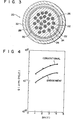
- Fig. 4 graphically compares the A.C. loss occurring in the superconductor 20 embodying this invention with that observed in the conventional superconductor 10 (Fig. 2) involving an Nb barrier wall 14.
- the ordinate shows the unit length of the superconductors 10, 20, and the A.C. loss Q per cycle (J/m-cycle).
- the abscissa denotes the maximum magnitude Bm(T) of a magnetic field supplied to the superconductors 10, 20.
- the A.C. loss was determined by the magnetic method whereby the superconductors 10, 20 were supplied with a pulse magnetic field whose magnitude was changed as 0(T) ⁇ Bm(T) + 0(T) at the liquid helium temperature (4.2°K).
- the A.C. loss occurring in the superconductor 20 embodying this invention was reduced to about half that observed in the conventional superconductor 10, proving that the present invention can provide a superconductor of extremely low A.C. loss.
- the superconductor of this invention involving the vanadium barrier wall, indicated substantially the same data as the conventional superconductor using the niobium (Nb) barrier wall. This means that the superconductor of the invention has a very high stability.
- the stabilizing region 32 was prepared from copper (Cu).
- said stabilizing region 32 can be formed of, for example, aluminum (At) or silver (Ag) which have a lower resistivity than the Cu-Sn alloy.
- the superconducting region 24 was prepared from Nb 3 Sn compound. The high magnetic field property of this subject superconductor can be improved by adding 1 to 2% by_weight of Ti to said Nb 3 Sn compound. This improvement is substantiated by the fact that, without Ti, the critical current density Ic.drops, whereas the magnetic field intensity-B exceeds 12 telas.
- the superconductor of the above-mentioned feature can be manufactured by applying a pipe of a Ti-bearing Cu-Sn alloy consisting of 85% by weight of Cu, 13% by weight of Sn and 2% by weight of Ti or a pipe of an Nb-Ti alloy consisting of 99% by weight of Nb and 1% by weight of Ti, or both pipes.
- Nb wires are embedded in the Cu-Sn alloy which, in turn, is surrounded, successively, by the vanadium barrier wall and Cu stabilizing region.
- the present invention is not limited to the above-mentioned construction of a superconductor, but, rather, admits of various modifications.
- a plurality of stabilizing Cu wires are surrounded by a partitioning vanadium pipe 44.
- Said vanadium pipe 44 is enclosed in a Cu-Sn alloy pipe 46 to provide a first group of wires 40.
- a plurality of niobium (Nb) wires 52 are wrapped in a Cu-Sn alloy pipe 54, producing a second group of wires 50.
- This second group of wires 50 is bundled around the first group of wires 40. Both groups of wires 40, 50 are then inserted into a Cu-Sn alloy pipe 48. Later, drawing and heat treatment are applied to provide a superconductor wire including a plurality of stabilizing regions occupying the control portion, and a further plurality of Nb Sn superconducting regions surrounding said plural stabilizing regions.
- a single core wire 56 is manufactured by inserting a niobium (Nb) wire 58 into a Cu-Sn alloy pipe 60, and drawing this composite wire through a metal die having a hexagonal cross section.
- a compact bundle of said plural hexagonal single core wires 56 is inserted into a Cu-Sn alloy pipe 62.
- Cu-Sn alloy fillers 64 are interposed in the interstices defined between the Cu-Sn alloy pipe 62 and the plural single core wires 56.
- the Cu-Sn alloy 62 and Nb wires 58 are compactly fitted into the cylindrical pipe 62.
- the cylindrical pipe 62 is inserted into a vanadium barrier pipe 66 which is subsequently wrapped in a stabilizing Cu pipe 68.
- drawing and heat treatment are applied to manufacture a superconductor according to the second embodiment of.this invention.
- the various wire members are fitted into the surrounding pipes with greater compactness, thus providing a high quality superconductor.
- the superconductor may be twisted in order to reduce the coupling loss resulting from the coupling current.
- the sectional shape of the superconductor is not limited to a circular one. It may be rectangular, in which case the advantages of the invention would not be impaired. More specifically, the superconductor may be so shaped in the drawing process and then be subjected to a low-temperature heat treatment.
Landscapes
- Superconductors And Manufacturing Methods Therefor (AREA)
Applications Claiming Priority (2)
| Application Number | Priority Date | Filing Date | Title |
|---|---|---|---|
| JP59148610A JPS6158107A (ja) | 1984-07-19 | 1984-07-19 | Nb3Sn化合物超電導線 |
| JP148610/84 | 1984-07-19 |
Publications (2)
| Publication Number | Publication Date |
|---|---|
| EP0169078A2 true EP0169078A2 (de) | 1986-01-22 |
| EP0169078A3 EP0169078A3 (de) | 1988-11-17 |
Family
ID=15456626
Family Applications (1)
| Application Number | Title | Priority Date | Filing Date |
|---|---|---|---|
| EP85305169A Withdrawn EP0169078A3 (de) | 1984-07-19 | 1985-07-19 | Von der Verbindung Nb3Sn hergestellter Supraleiter |
Country Status (2)
| Country | Link |
|---|---|
| EP (1) | EP0169078A3 (de) |
| JP (1) | JPS6158107A (de) |
Cited By (2)
| Publication number | Priority date | Publication date | Assignee | Title |
|---|---|---|---|---|
| GB2246727A (en) * | 1990-07-06 | 1992-02-12 | Nat Res Dev | Method of fabricating an elongated artefact. |
| WO2025214655A1 (de) * | 2024-04-09 | 2025-10-16 | Bruker Eas Gmbh | SUBELEMENT FÜR EINEN HALBZEUGDRAHT ZUR HERSTELLUNG EINES Nb3Sn-SUPRALEITERDRAHTS |
Family Cites Families (3)
| Publication number | Priority date | Publication date | Assignee | Title |
|---|---|---|---|---|
| GB1394724A (en) * | 1972-08-04 | 1975-05-21 | Atomic Energy Authority Uk | Superconducting members and methods of mahufacture thereof |
| US3958327A (en) * | 1974-05-01 | 1976-05-25 | Airco, Inc. | Stabilized high-field superconductor |
| FR2334182A1 (fr) * | 1975-12-03 | 1977-07-01 | Furukawa Electric Co Ltd | Cable comportant un compose supraconducteur et procede de fabrication d'un tel cable |
-
1984
- 1984-07-19 JP JP59148610A patent/JPS6158107A/ja active Pending
-
1985
- 1985-07-19 EP EP85305169A patent/EP0169078A3/de not_active Withdrawn
Cited By (4)
| Publication number | Priority date | Publication date | Assignee | Title |
|---|---|---|---|---|
| GB2246727A (en) * | 1990-07-06 | 1992-02-12 | Nat Res Dev | Method of fabricating an elongated artefact. |
| GB2246727B (en) * | 1990-07-06 | 1994-01-26 | Nat Res Dev | Method of fabricating an elongated artefact |
| US5369873A (en) * | 1990-07-06 | 1994-12-06 | British Technology Group Ltd. | Method of fabricating an elongated artefact |
| WO2025214655A1 (de) * | 2024-04-09 | 2025-10-16 | Bruker Eas Gmbh | SUBELEMENT FÜR EINEN HALBZEUGDRAHT ZUR HERSTELLUNG EINES Nb3Sn-SUPRALEITERDRAHTS |
Also Published As
| Publication number | Publication date |
|---|---|
| JPS6158107A (ja) | 1986-03-25 |
| EP0169078A3 (de) | 1988-11-17 |
Similar Documents
| Publication | Publication Date | Title |
|---|---|---|
| US20050178472A1 (en) | Method for producing (Nb, Ti)3Sn wire by use of Ti source rods | |
| JP2897776B2 (ja) | ワイヤ又はケーブル形態の電気導線 | |
| US3996661A (en) | Method for the manufacture of a superconductor having an intermetallic two element compound | |
| JPH0261764B2 (de) | ||
| US3836404A (en) | Method of fabricating composite superconductive electrical conductors | |
| US4153986A (en) | Method for producing composite superconductors | |
| JP2019186167A (ja) | Nb3Sn超電導線材の前駆体及びNb3Sn超電導線材 | |
| EP0169078A2 (de) | Von der Verbindung Nb3Sn hergestellter Supraleiter | |
| US3996662A (en) | Method for the manufacture of a superconductor having an intermetallic two element compound | |
| Yoshizaki et al. | Nb 3 Sn superconducting cables processed by internal tin diffusion | |
| JP2910586B2 (ja) | Nb▲3▼Sn超電導線材 | |
| JPH0570888B2 (de) | ||
| JP3425018B2 (ja) | Nb3Al系多芯超電導線 | |
| JP3505894B2 (ja) | 化合物系超電導線材 | |
| EP0076365A1 (de) | Supraleitende Energiekabel | |
| JP2878390B2 (ja) | 超電導発電機用Nb▲下3▼Sn超電導線の製造方法 | |
| Scanlan et al. | Multifilamentary Nb 3 Sn for superconducting generator applications | |
| JP2926774B2 (ja) | 交流用Nb▲下3▼Sn多芯超電導線 | |
| JP4174890B2 (ja) | 酸化物多芯超電導線材の製造方法 | |
| JPH087681A (ja) | A3 b型化合物超電導線およびその製造方法 | |
| JP3045517B2 (ja) | 化合物系超電導撚線およびその製造方法 | |
| JP2742421B2 (ja) | 超電導線およびその製造方法 | |
| JPH04132108A (ja) | Nb↓3Al系超電導導体 | |
| JPH04298914A (ja) | 化合物超電導導体 | |
| JPS62271308A (ja) | 超電導ケ−ブル導体 |
Legal Events
| Date | Code | Title | Description |
|---|---|---|---|
| PUAI | Public reference made under article 153(3) epc to a published international application that has entered the european phase |
Free format text: ORIGINAL CODE: 0009012 |
|
| 17P | Request for examination filed |
Effective date: 19850805 |
|
| AK | Designated contracting states |
Designated state(s): DE FR GB |
|
| PUAL | Search report despatched |
Free format text: ORIGINAL CODE: 0009013 |
|
| AK | Designated contracting states |
Kind code of ref document: A3 Designated state(s): DE FR GB |
|
| 17Q | First examination report despatched |
Effective date: 19910218 |
|
| STAA | Information on the status of an ep patent application or granted ep patent |
Free format text: STATUS: THE APPLICATION IS DEEMED TO BE WITHDRAWN |
|
| 18D | Application deemed to be withdrawn |
Effective date: 19910829 |
|
| RIN1 | Information on inventor provided before grant (corrected) |
Inventor name: MURASE, SATORUC/O PATENT DIVISION Inventor name: KOIZUMI, MISAOC/O PATENT DIVISION |