EP0169089A1 - Elementare Datenverarbeitungsvorrichtung - Google Patents
Elementare Datenverarbeitungsvorrichtung Download PDFInfo
- Publication number
- EP0169089A1 EP0169089A1 EP85400952A EP85400952A EP0169089A1 EP 0169089 A1 EP0169089 A1 EP 0169089A1 EP 85400952 A EP85400952 A EP 85400952A EP 85400952 A EP85400952 A EP 85400952A EP 0169089 A1 EP0169089 A1 EP 0169089A1
- Authority
- EP
- European Patent Office
- Prior art keywords
- register
- output
- input
- initial
- bit
- Prior art date
- Legal status (The legal status is an assumption and is not a legal conclusion. Google has not performed a legal analysis and makes no representation as to the accuracy of the status listed.)
- Granted
Links
Images
Classifications
-
- G—PHYSICS
- G06—COMPUTING OR CALCULATING; COUNTING
- G06F—ELECTRIC DIGITAL DATA PROCESSING
- G06F5/00—Methods or arrangements for data conversion without changing the order or content of the data handled
- G06F5/01—Methods or arrangements for data conversion without changing the order or content of the data handled for shifting, e.g. justifying, scaling, normalising
Definitions
- the present invention relates to an elementary device for processing digital information, comprising: on the one hand a shift register of determined length composed of cells in number corresponding to this length, arranged in series between an input and an output of this register, and each of which contains, at an initial instant, a bit of an initial word, the first bit of which is contained in the input cell and the last bit of which is in the output cell; and on the other hand, control means, synchronized with this initial instant to allow, from the start of an exploitation phase of the initial word, to have, at the output of the register, a series of relevant bits comprising certain at least successive bits forming this initial word, with a certain temporal offset with respect to the initial instant and / or starting from a relevant bit having a certain spatial offset, along the length of the register, with respect to the last bit of the initial word, these control means comprising a clock producing pulses at the rate of which the bits progress from one cell to another in the direction of the output of the register.
- Shift registers are well known elements, the use of which is extremely frequent and practically essential in serial type data processing circuits.
- arithmetic and logical unit operates combinations of binary information
- the registers affect temporary storage of information, divisions, concatenations and / or offsets
- the control unit ensures the organization over time of the various elementary operations.
- registers exchange, bit by bit, digital information with the arithmetic and logic unit, under the control of the control unit.
- the control unit notably comprises a clock producing primary pulses at a fixed base frequency, as well as frequency dividers producing secondary clock pulses at the base frequency divided by a power of 2, and combinational circuits with logic gates which deliver, from the primary and secondary clock pulses, more or less complex control signals having various phase shifts between them and to which specific control functions are assigned.
- the lengths of the different registers are often equal to each other, and for example equal to 8, or at least often represented by a power of 2.
- Each bit of a binary word contained in a shift register is representative of a determined value at a determined instant, and this value can be modified at a following instant, in particular by a shift of the word in the register, controlled by l 'control unit.
- control unit must contain, practically for each shift register, a combinatorial circuit for developing the control signals specific to this register, and on the other hand that this combinatorial circuit can have a structure. relatively complex, in particular when the amplitude of the offset to be performed does not correspond to a number of clock pulses represented by a power of 2.
- the aim of the present invention is to propose an elementary data processing device capable of shifting digital information either in space, that is to say by a change of position, or in time, that is to say by a delay, with means of control as simple as possible.
- the device of the invention which comprises on the one hand a shift register of determined length composed of cells in number corresponding to this length, arranged in series between an input and an output of this register, and each of which contains, at an initial time, a bit of an initial word, the first bit of which is contained in the input cell and the last bit of which is in the output cell; and on the other hand, control means to locate this initial instant and to allow, from the start of an exploitation phase of the initial word, to have, at the output of the register, a series of relevant bits comprising certain at least successive bits forming this initial word, with a certain time offset with respect to the initial instant and / or starting from a bit relevant having a certain spatial offset, along the length of the register, with respect to the last bit of the initial word, these control means comprising a clock producing pulses at the rate of which the bits progress from one cell to another in the direction of the output of the register, is essentially characterized in that these control means comprise at least one auxiliary register output, on which is entered the series
- the device of the invention further comprises a second shift register whose input is connected to an auxiliary output of the first register, and this second register, which is intended to contain in its last cell , at the end of the phase of exploitation of the initial word contained in the first register at the initial time, the last relevant bit of this initial word, has a length equal to that of the first register, the end of said phase of exploitation being thus identified from said initial instant by the passage of a time corresponding to the appearance of a number of clock pulses equal to the number of cells of each of these first and second registers.
- Frequency dividers and combinational circuits forming part of the control unit are thus greatly simplified insofar as it is sufficient for these circuits to take account only of the lengths of the registers, which are generally equal to each other and represented by a power of 2.
- the shift register is a dynamic register looped on itself by connection of its main output with its input , so as to allow permanent recirculation of the digital information it contains, and the auxiliary output of this register is separated from the input or the output of the register by a number of cells equal to the number of clock pulses representing said time offset.
- the desired digital information is available at the desired time on the auxiliary output of the register without it being necessary to provide any combinative circuit capable of identifying the instant when the information output from the register is relevant. , that is to say constitute the desired information.
- the device comprises, in addition to the shift register, a controllable multiplexer with at least two inputs and one output, this output being capable of being selectively connected, as a function of a signal control applied to this multiplexer, to any of inputs of the latter, this multiplexer being, by its inputs, connected to at least two respective outputs of the shift register, at least one of which is an auxiliary output.
- the device then constitutes, between the input of the shift register and the output of the multiplexer, for a stream of digital information applied to the input of the shift register, a buffer register introducing into this stream of information a programmable delay, determined by the value of said control signal.
- the device of the invention is particularly applicable to data processing units for specific use and with simple programming, such as for example programmable digital filters.
- An even more particular application is that of programmable digital bandpass filters based on 2nd order filter cells and capable of being used in centralized remote control receivers.
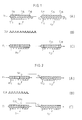
- FIG. 1A represents two conventional shift registers R1 and R2, comprising inputs E1, E2 and respective main outputs SP1, SP2, the input E2 of the second register R2 being connected to the output SP1 of the first register R1.
- Each register is constituted by a succession of flip-flops, such as Cll, C15, C18, C21, C28, which can be considered as elementary memory cells intended to store a bit of the binary word contained, at a given time, in the register .
- the register R1 contains the binary word 10110010 and the register R2 contains a binary word, relevant or not for the calculations to be carried out, but indifferent for the present description, and symbolized by XXXXXXXX.
- the shift registers RI and R2 are controlled in a well-known manner by the application, on their respective control inputs EC1 and EC2, of a common clock signal CLK coming from a clock (not shown).
- the bits of the words contained in the registers are transferred from one cell to another in the direction of the respective main outputs SP1, SP2 of these registers. Because of the link existing between the output SP1 of the first register and the input E2 of the second, the bits pushed at the output of the first register are recovered in the first cell C21 of the second register.
- the bits received at the input El of the first register are relevant or not with respect to the calculations to be carried out, but indifferent for the present description, and are represented by X.
- the first register RI can, as is known per se, be preceded by a sign extension multiplexer, capable of copying the bit contained at the initial instant in the first cell C11.
- the frequency of the clock pulses CLK is called F
- F the frequency of the clock pulses CLK
- the 11 clock pulses will for example be produced by a combinative circuit realizing the boolean function: CLK AND (W OR ((X AND Y) OR (X AND Z))).
- FIG. 2 represents the means of the invention, which make it possible to achieve the same result in a much simpler manner.
- the transition from the configuration of FIG. 2A to the configuration 2C can no longer be carried out by means of 11 clock pulses, but by 8 clock pulses, in other words d 'a number of clock pulses equal to the number of cells in each of the registers RI and R2.
- this number is itself chosen, conventionally, equal to a power of 2 (generally equal to 8), the control of these registers is significantly reduced.
- the control signal from FIG. 2B is expressed by the simple boolean combination: CLK AND W, and this whatever the shift that we want to achieve, that is to say whatever the position of the auxiliary output SA1 on the register Rl .
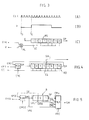
- FIG. 3 represents a static shift register RS containing a binary word "10110010" which, with respect to a phenomenon occurring at an initial instant To, must be delayed so as to be made available, bit after bit, only from an instant TE, after To and marking the beginning of an exploitation phase of this initial binary word "10110010".
- static shift register is meant a shift register consisting of static type D flip-flops.
- MOS Metal Oxide Semi-conductor
- D flip-flops can be static or dynamic, the latter being distinguished from the former in that they are produced with half the transistors but require permanent refreshment of the information they contain.
- the desired time offset (of 4 clock pulses in the example of FIG. 3) between the initial instant To and the start TE of the operating phase is obtained by producing, by boolean combination of the primary clock signal CLK and secondary clock signals of frequency multiple of that of this primary signal, a validation signal V having the desired time offset TE-To with respect to To.
- this signal V may, in the general case, require relatively complex means.
- This signal V combined with the clock signal CLK by means of an AND logic gate, designated by PL, is applied to the input of EC command of the RS register, so that the binary word "10110010", contained in this register at the initial time To does not start to shift until from the time TE, and at this time TE the bit available at the output of the register is indeed the last bit of the initial binary word.
- FIG. 4 represents the means of the invention which make it possible to achieve the same result in a simpler manner.
- the register RD is a dynamic register whose output SP is, in a known manner, looped back to the input E through a multiplexer MUX.
- the multiplexer MUX includes a recycling input EM2 connected to the output SP of the register RD, a new data input EM1, an output SM connected to the input E of the register, and a control input EMC capable of receiving a signal allowing, selectively, to connect the output SM to the input EM1 for the introduction of new data into the register RD, or to the input EM2 for the recycling of data already contained in this register.
- the register itself comprises, as usual, an input EC for shift timing control receiving a clock signal such as the signal CLK of FIG. 3A.
- the signal EMC is for example fixed, during the whole cycle represented by the 16 clock pulses illustrated in FIG. 3A, at a value such that the output SM of the multiplexer is connected to the recycling input EM2.
- the bit by bit provision of the initial word 10110010 from time TE is simply carried out by providing an auxiliary output SA at cell C4 which, at time TE, will contain the last bit of the binary word 10110010; from the instant TE, a circuit connected to the auxiliary output SA of the register RD can therefore read bit by bit the word "10110010" from the last bit of this word; if L designates the length of the register (i.e. the number of its cells), the auxiliary output SA of the register RD is separated from the input of the latter by a number of cells equal to (TE-To) modulo L where (TE-To) is the interval between the instants TE and To, measured in number of clock pulses.
- the arrangement would therefore have been the same as that of FIG. 4 if, instead of using the word 10110010 from the instant TE, we had wanted to use it from a later instant, separated from TE by a number of clock pulses equal to a multiple of the number of cells in the register, for example TE + L or TE + 2L, the same configuration of bits being found at all these times in the register RD as long as the latter remains buckled up on itself.
- time offset between TE and To could have been set to a value other than that which corresponds to FIG. 3B by placing the auxiliary output SA at another location along the length of the register RD, that is to say at the output of a cell other than cell C4.
- FIG. 5 represents a device according to the invention, making it possible to constitute, for a stream of digital information in series, a programmable delay buffer register.
- This device comprises a shift register R comprising a data input E, a main output SP and auxiliary outputs SAO, SA1 and SA2; for the sake of clarity of the drawing, the command input EC of the register R and the associated links have not been shown in FIG. 5; the output SAO coincides for example with the input E of this register R, and the outputs SAO to SP are connected to the respective inputs EMO to EM3 of a multiplexer MUX comprising, in addition to these four data inputs EMO to EM3, an EMC control input and an SM output.
- the multiplexer MUX known per se, makes it possible, by application of an appropriate signal to its input EMC, to selectively connect the output SM to any one of the inputs EMO to EM3.
- the control input EMC comprises, as is known per se, several conductors so as to allow the addressing of these inputs of data by means of a multi-bit signal injected in parallel on these conductors.
- a stream of binary digital information arriving at the input E of the register R can be recovered on the output SM of the multiplexer MUX, according to the signal applied to the input EMC of the latter, either in having taken the SAO-EMO path, that is to say without any delay, either by having taken the SA1-EM1 path, that is to say with a delay of a clock pulse corresponding to the temporary storage of each bit of the information flow in the first cell of the register (the cell on the left), either by taking the path SA2-EM2, that is to say with a delay of 2 clock pulses corresponding to the storage temporary of each bit of the information flow in the first two cells of the register, that is to say finally having taken the path SP-EM3, that is to say with a delay of 3 clock pulses corresponding to the temporary storage of each bit of the information flow in each of the cells of register R.
- the number of cells of this re gistre is not limited to 3, but is chosen, as will be apparent to those skilled in the art, according to the needs to be
- the shift register R can, as is known per se, be preceded by a sign extension multiplexer MUXO of which an input EM10 can receive new information, and of which another input EM20 is connected to an extension output SE sign provided on the first cell of register R; this sign extension multiplexer MUXO furthermore comprises an output SMO connected to the input E of the register R and an control input EMCO capable of receiving a signal making it possible to selectively connect the output SMO to the input EM10 in view the reception of a stream of new information, or at the input EM20 so as to replace, at the appearance of a clock pulse, the bit initially contained in the first cell of the register R by an identical bit .
Landscapes
- Engineering & Computer Science (AREA)
- Theoretical Computer Science (AREA)
- Physics & Mathematics (AREA)
- General Engineering & Computer Science (AREA)
- General Physics & Mathematics (AREA)
- Synchronisation In Digital Transmission Systems (AREA)
- Pulse Circuits (AREA)
- Logic Circuits (AREA)
Applications Claiming Priority (2)
| Application Number | Priority Date | Filing Date | Title |
|---|---|---|---|
| FR8407845A FR2564619B1 (fr) | 1984-05-21 | 1984-05-21 | Dispositif elementaire de traitement de donnees |
| FR8407845 | 1984-05-21 |
Publications (2)
| Publication Number | Publication Date |
|---|---|
| EP0169089A1 true EP0169089A1 (de) | 1986-01-22 |
| EP0169089B1 EP0169089B1 (de) | 1990-07-11 |
Family
ID=9304192
Family Applications (1)
| Application Number | Title | Priority Date | Filing Date |
|---|---|---|---|
| EP85400952A Expired - Lifetime EP0169089B1 (de) | 1984-05-21 | 1985-05-15 | Elementare Datenverarbeitungsvorrichtung |
Country Status (7)
| Country | Link |
|---|---|
| US (1) | US4796225A (de) |
| EP (1) | EP0169089B1 (de) |
| AU (1) | AU577858B2 (de) |
| DE (1) | DE3578610D1 (de) |
| FR (1) | FR2564619B1 (de) |
| GR (1) | GR851221B (de) |
| ZA (1) | ZA853838B (de) |
Families Citing this family (3)
| Publication number | Priority date | Publication date | Assignee | Title |
|---|---|---|---|---|
| JP2982902B2 (ja) * | 1987-06-16 | 1999-11-29 | 三菱電機株式会社 | 半導体メモリ |
| DE10208618A1 (de) * | 2002-02-27 | 2003-09-04 | Bosch Gmbh Robert | Digitale Verzögerungsleitung |
| US7184705B2 (en) | 2002-03-08 | 2007-02-27 | Telefonaktiebolaget Lm Ericsson (Publ) | Distributed MAC in an uncoordinated radio environment |
Citations (2)
| Publication number | Priority date | Publication date | Assignee | Title |
|---|---|---|---|---|
| US2925218A (en) * | 1953-11-20 | 1960-02-16 | Ibm | Instruction controlled shifting device |
| GB2119976A (en) * | 1982-04-22 | 1983-11-23 | Tokyo Shibaura Electric Co | Shift circuit |
Family Cites Families (12)
| Publication number | Priority date | Publication date | Assignee | Title |
|---|---|---|---|---|
| US3156901A (en) * | 1960-12-29 | 1964-11-10 | Rca Corp | Shift register systems |
| US3278904A (en) * | 1962-06-20 | 1966-10-11 | Gen Precision Inc | High speed serial arithmetic unit |
| DE1249320B (de) * | 1964-12-23 | |||
| US3478325A (en) * | 1967-01-16 | 1969-11-11 | Ibm | Delay line data transfer apparatus |
| US3596187A (en) * | 1969-11-26 | 1971-07-27 | William J Thompson | Pulse code generator |
| US3656122A (en) * | 1969-12-11 | 1972-04-11 | Bell Telephone Labor Inc | TIME-SHARED SHIFT REGISTER COUNTER WITH COUNT MODIFIED EACH Nth RECIRCULATION |
| GB1468753A (en) * | 1974-05-09 | 1977-03-30 | Honeywell Invormation Systems | Associative memory |
| JPS53112040A (en) * | 1977-03-11 | 1978-09-30 | Citizen Watch Co Ltd | Shift register circuit |
| US4176400A (en) * | 1977-08-10 | 1979-11-27 | Teletype Corporation | Buffer storage and control |
| US4524455A (en) * | 1981-06-01 | 1985-06-18 | Environmental Research Inst. Of Michigan | Pipeline processor |
| JPS58121458A (ja) * | 1981-12-09 | 1983-07-19 | Fujitsu Ltd | スキヤンアウト方式 |
| DE3368770D1 (en) * | 1982-11-20 | 1987-02-05 | Int Computers Ltd | Testing digital electronic circuits |
-
1984
- 1984-05-21 FR FR8407845A patent/FR2564619B1/fr not_active Expired
-
1985
- 1985-05-15 EP EP85400952A patent/EP0169089B1/de not_active Expired - Lifetime
- 1985-05-15 DE DE8585400952T patent/DE3578610D1/de not_active Expired - Fee Related
- 1985-05-17 US US06/735,238 patent/US4796225A/en not_active Expired - Fee Related
- 1985-05-20 GR GR851221A patent/GR851221B/el unknown
- 1985-05-20 AU AU42666/85A patent/AU577858B2/en not_active Ceased
- 1985-05-21 ZA ZA853838A patent/ZA853838B/xx unknown
Patent Citations (2)
| Publication number | Priority date | Publication date | Assignee | Title |
|---|---|---|---|---|
| US2925218A (en) * | 1953-11-20 | 1960-02-16 | Ibm | Instruction controlled shifting device |
| GB2119976A (en) * | 1982-04-22 | 1983-11-23 | Tokyo Shibaura Electric Co | Shift circuit |
Also Published As
| Publication number | Publication date |
|---|---|
| AU4266685A (en) | 1985-11-28 |
| ZA853838B (en) | 1986-01-29 |
| FR2564619B1 (fr) | 1986-09-26 |
| EP0169089B1 (de) | 1990-07-11 |
| US4796225A (en) | 1989-01-03 |
| DE3578610D1 (de) | 1990-08-16 |
| AU577858B2 (en) | 1988-10-06 |
| FR2564619A1 (fr) | 1985-11-22 |
| GR851221B (de) | 1985-11-25 |
Similar Documents
| Publication | Publication Date | Title |
|---|---|---|
| EP3252774B1 (de) | Adaptierter speicherschaltkreis zur durchführung von rechenoperationen | |
| WO1999060494A1 (fr) | Systeme d'acquisition de donnees comprenant un circuit de conversion d'un signal d'entree analogique haute frequence en une pluralite de signaux numeriques | |
| EP0006478A1 (de) | Programmierbarer Steuerschalter für ein Datenverarbeitungssystem | |
| EP3376670B1 (de) | Konfigurierbare verzögerungsleitung | |
| EP0169089B1 (de) | Elementare Datenverarbeitungsvorrichtung | |
| EP0475862B1 (de) | Schneller Zähler/Teiler und dessen Verwendung in einem Zähler mit Impulsunterdrückung | |
| EP0476592A2 (de) | Adressengenerator für den Datenspeicher eines Prozessors | |
| EP0246135B1 (de) | Phasen- und Frequenzdetektor und seine Anwendung in einer Phasenregelschleife | |
| EP0327445A1 (de) | Allgemeiner digitaler Multiplizierer und digitaler Filter mit diesem Multiplizierer | |
| EP0341097B1 (de) | Rekursiver Addierer zur Berechnung der Summe zweier Operanden | |
| EP0400734B1 (de) | Programmierbares Binärsignal-Verzögerungsverfahren und Anwendung auf ein Fehlerkorrigierkode-Verfahren | |
| EP0842465B1 (de) | Organisationssystem und verfahren zur reihenfolgebestimmung der schaltungen eines mikroprozessors | |
| EP0889481A1 (de) | Verbesserungen von Speicherschaltungen mit sequentiellem Zugriff | |
| CH622901A5 (de) | ||
| EP1445865A1 (de) | Frequenzteiler mit Trichterstruktur | |
| EP0449190B1 (de) | Programmschalteinrichtung zur Erzeugung von binären Ausgangssignalen als Reaktion auf ein Taktsignal | |
| FR2773652A1 (fr) | Circuit de generation d'un signal d'activation commande | |
| FR2765718A1 (fr) | Memoire a acces sequentiels a faible consommation | |
| EP0643394B1 (de) | Schreib-/Lesetaktvergleichungsanordnung für einen Pufferspeicher | |
| EP0962855A1 (de) | Schnell Zugriffzeit in Pufferschaltungen | |
| EP0592260B1 (de) | Zählschaltung für Frequenzteilung und Synthetisierer mit einer derartigen Schaltung | |
| FR2710777A1 (fr) | Dispositif électronique de mémoire à accès séquentiel. | |
| EP0218527B1 (de) | Schaltwerk, insbesondere für logische Schaltungen | |
| EP0419381B1 (de) | Absolutwertbestimmungsschaltung für Vorzeichenzifferzahlen mit Grundzahl 2 | |
| EP1235225A2 (de) | Verfahren und Anordnung für serielle Speicherauslesung mit Adressensprung |
Legal Events
| Date | Code | Title | Description |
|---|---|---|---|
| PUAI | Public reference made under article 153(3) epc to a published international application that has entered the european phase |
Free format text: ORIGINAL CODE: 0009012 |
|
| AK | Designated contracting states |
Designated state(s): BE CH DE GB LI NL SE |
|
| 17P | Request for examination filed |
Effective date: 19860225 |
|
| RAP1 | Party data changed (applicant data changed or rights of an application transferred) |
Owner name: SCHLUMBERGER INDUSTRIES |
|
| 17Q | First examination report despatched |
Effective date: 19890307 |
|
| GRAA | (expected) grant |
Free format text: ORIGINAL CODE: 0009210 |
|
| AK | Designated contracting states |
Kind code of ref document: B1 Designated state(s): BE CH DE GB LI NL SE |
|
| REF | Corresponds to: |
Ref document number: 3578610 Country of ref document: DE Date of ref document: 19900816 |
|
| GBT | Gb: translation of ep patent filed (gb section 77(6)(a)/1977) | ||
| PLBE | No opposition filed within time limit |
Free format text: ORIGINAL CODE: 0009261 |
|
| STAA | Information on the status of an ep patent application or granted ep patent |
Free format text: STATUS: NO OPPOSITION FILED WITHIN TIME LIMIT |
|
| 26N | No opposition filed | ||
| EAL | Se: european patent in force in sweden |
Ref document number: 85400952.9 |
|
| PGFP | Annual fee paid to national office [announced via postgrant information from national office to epo] |
Ref country code: SE Payment date: 19970417 Year of fee payment: 13 |
|
| PGFP | Annual fee paid to national office [announced via postgrant information from national office to epo] |
Ref country code: CH Payment date: 19970424 Year of fee payment: 13 |
|
| PGFP | Annual fee paid to national office [announced via postgrant information from national office to epo] |
Ref country code: GB Payment date: 19970501 Year of fee payment: 13 |
|
| PGFP | Annual fee paid to national office [announced via postgrant information from national office to epo] |
Ref country code: BE Payment date: 19970529 Year of fee payment: 13 |
|
| PGFP | Annual fee paid to national office [announced via postgrant information from national office to epo] |
Ref country code: NL Payment date: 19970531 Year of fee payment: 13 |
|
| PGFP | Annual fee paid to national office [announced via postgrant information from national office to epo] |
Ref country code: DE Payment date: 19970702 Year of fee payment: 13 |
|
| PG25 | Lapsed in a contracting state [announced via postgrant information from national office to epo] |
Ref country code: GB Free format text: LAPSE BECAUSE OF NON-PAYMENT OF DUE FEES Effective date: 19980515 |
|
| PG25 | Lapsed in a contracting state [announced via postgrant information from national office to epo] |
Ref country code: SE Free format text: LAPSE BECAUSE OF NON-PAYMENT OF DUE FEES Effective date: 19980516 |
|
| PG25 | Lapsed in a contracting state [announced via postgrant information from national office to epo] |
Ref country code: LI Free format text: LAPSE BECAUSE OF NON-PAYMENT OF DUE FEES Effective date: 19980531 Ref country code: CH Free format text: LAPSE BECAUSE OF NON-PAYMENT OF DUE FEES Effective date: 19980531 Ref country code: BE Free format text: LAPSE BECAUSE OF NON-PAYMENT OF DUE FEES Effective date: 19980531 |
|
| BERE | Be: lapsed |
Owner name: SCHLUMBERGER INDUSTRIES Effective date: 19980531 |
|
| PG25 | Lapsed in a contracting state [announced via postgrant information from national office to epo] |
Ref country code: NL Free format text: LAPSE BECAUSE OF NON-PAYMENT OF DUE FEES Effective date: 19981201 |
|
| GBPC | Gb: european patent ceased through non-payment of renewal fee |
Effective date: 19980515 |
|
| REG | Reference to a national code |
Ref country code: CH Ref legal event code: PL |
|
| EUG | Se: european patent has lapsed |
Ref document number: 85400952.9 |
|
| NLV4 | Nl: lapsed or anulled due to non-payment of the annual fee |
Effective date: 19981201 |
|
| PG25 | Lapsed in a contracting state [announced via postgrant information from national office to epo] |
Ref country code: DE Free format text: LAPSE BECAUSE OF NON-PAYMENT OF DUE FEES Effective date: 19990302 |