EP0962855A1 - Schnell Zugriffzeit in Pufferschaltungen - Google Patents
Schnell Zugriffzeit in Pufferschaltungen Download PDFInfo
- Publication number
- EP0962855A1 EP0962855A1 EP99401300A EP99401300A EP0962855A1 EP 0962855 A1 EP0962855 A1 EP 0962855A1 EP 99401300 A EP99401300 A EP 99401300A EP 99401300 A EP99401300 A EP 99401300A EP 0962855 A1 EP0962855 A1 EP 0962855A1
- Authority
- EP
- European Patent Office
- Prior art keywords
- register
- circuit
- buffer circuit
- data
- buffer
- Prior art date
- Legal status (The legal status is an assumption and is not a legal conclusion. Google has not performed a legal analysis and makes no representation as to the accuracy of the status listed.)
- Granted
Links
Images

Classifications
-
- G—PHYSICS
- G06—COMPUTING OR CALCULATING; COUNTING
- G06F—ELECTRIC DIGITAL DATA PROCESSING
- G06F5/00—Methods or arrangements for data conversion without changing the order or content of the data handled
- G06F5/06—Methods or arrangements for data conversion without changing the order or content of the data handled for changing the speed of data flow, i.e. speed regularising or timing, e.g. delay lines, FIFO buffers; over- or underrun control therefor
- G06F5/10—Methods or arrangements for data conversion without changing the order or content of the data handled for changing the speed of data flow, i.e. speed regularising or timing, e.g. delay lines, FIFO buffers; over- or underrun control therefor having a sequence of storage locations each being individually accessible for both enqueue and dequeue operations, e.g. using random access memory
-
- G—PHYSICS
- G06—COMPUTING OR CALCULATING; COUNTING
- G06F—ELECTRIC DIGITAL DATA PROCESSING
- G06F3/00—Input arrangements for transferring data to be processed into a form capable of being handled by the computer; Output arrangements for transferring data from processing unit to output unit, e.g. interface arrangements
- G06F3/06—Digital input from, or digital output to, record carriers, e.g. RAID, emulated record carriers or networked record carriers
- G06F3/0601—Interfaces specially adapted for storage systems
- G06F3/0602—Interfaces specially adapted for storage systems specifically adapted to achieve a particular effect
- G06F3/061—Improving I/O performance
- G06F3/0613—Improving I/O performance in relation to throughput
-
- G—PHYSICS
- G06—COMPUTING OR CALCULATING; COUNTING
- G06F—ELECTRIC DIGITAL DATA PROCESSING
- G06F3/00—Input arrangements for transferring data to be processed into a form capable of being handled by the computer; Output arrangements for transferring data from processing unit to output unit, e.g. interface arrangements
- G06F3/06—Digital input from, or digital output to, record carriers, e.g. RAID, emulated record carriers or networked record carriers
- G06F3/0601—Interfaces specially adapted for storage systems
- G06F3/0628—Interfaces specially adapted for storage systems making use of a particular technique
- G06F3/0655—Vertical data movement, i.e. input-output transfer; data movement between one or more hosts and one or more storage devices
- G06F3/0656—Data buffering arrangements
-
- G—PHYSICS
- G06—COMPUTING OR CALCULATING; COUNTING
- G06F—ELECTRIC DIGITAL DATA PROCESSING
- G06F3/00—Input arrangements for transferring data to be processed into a form capable of being handled by the computer; Output arrangements for transferring data from processing unit to output unit, e.g. interface arrangements
- G06F3/06—Digital input from, or digital output to, record carriers, e.g. RAID, emulated record carriers or networked record carriers
- G06F3/0601—Interfaces specially adapted for storage systems
- G06F3/0628—Interfaces specially adapted for storage systems making use of a particular technique
- G06F3/0655—Vertical data movement, i.e. input-output transfer; data movement between one or more hosts and one or more storage devices
- G06F3/0658—Controller construction arrangements
-
- G—PHYSICS
- G06—COMPUTING OR CALCULATING; COUNTING
- G06F—ELECTRIC DIGITAL DATA PROCESSING
- G06F3/00—Input arrangements for transferring data to be processed into a form capable of being handled by the computer; Output arrangements for transferring data from processing unit to output unit, e.g. interface arrangements
- G06F3/06—Digital input from, or digital output to, record carriers, e.g. RAID, emulated record carriers or networked record carriers
- G06F3/0601—Interfaces specially adapted for storage systems
- G06F3/0668—Interfaces specially adapted for storage systems adopting a particular infrastructure
- G06F3/0671—In-line storage system
- G06F3/0673—Single storage device
- G06F3/0674—Disk device
Definitions
- the subject of the present invention is a circuit buffer with means allowing under certain conditions rapid access to data contained in this buffer circuit.
- One of the favorite applications of buffer circuit according to the invention is intended for a use in an external memory interface of a complex circuit such as a microprocessor.
- the external memory interface can constitute with the microprocessor a circuit monolithic.
- External memory interfaces of circuits complexes such as microprocessors have to manage communications with these complex circuits in two directions: from the microprocessor to the interface external memory and external memory interface to the microprocessor.
- Communications take place in the form exchange of information, most often by via a cable connection called bus bidirectional transmission.
- This information can be memory addresses, data, or even ordering instructions.
- Information circulates in the form of data binaries. This binary data constitutes words. Information flows from the microprocessor to the external memory interface when requests access to external memory are issued by the microprocessor. Information flows from the external memory interface to the microprocessor when the appropriate responses to these requests are returned. In both cases, the information circulate by means of the transmission bus.
- the external memory interface must therefore have two buffer circuits: an input buffer circuit and an output buffer circuit.
- External memory access requests issued by the microprocessor are stored in the circuit external memory interface input buffer. These requests are then decoded by the memory interface external. Thanks to this decoding, the addresses are obtained memories to be accessed as well as the type access required: it can be a mode access write or access in read mode. Actual access to the external memory is then only effective. In in the case of a reading from the external memory, a word read is stored in the output buffer circuit of the external memory interface. It is then transmitted to the microprocessor by means of the bus transmission.
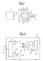
- Figure 1 shows a block diagram of the elements essentials involved in the exchange of information between a complex microprocessor-type circuit and an external memory interface.
- a microprocessor 1 is connected to an interface of external memory 2 by means of a transmission bus 22.
- This transmission bus 22 carries the data up to buffer circuit 3 of the memory interface external 2.
- the buffer circuit 3 consists of a input buffer circuit 4 and a buffer circuit of output 5.
- the input buffer circuit 4 receives the microprocessor access requests 1.
- the circuit output buffer 5 issues responses to these requests after a treatment carried out: a memory space 7 of a external memory 8, targeted by the request, can be read, written or erased using memory access 6.
- Figure 2 shows an input buffer circuit known from an external memory interface.
- FIG. 2 The diagram shown in Figure 2 is a circuit state of the art input buffer 20.
- This input buffer circuit 20 can be of the circuit type input buffer 4 contained in the memory interface described in Figure 1.
- the input buffer circuit 20 receives at an input 21 the transmission bus 22. Requests for access to the external memory transported by the transmission bus 22 are received by a bus interface 23. This register type bus interface 23 provides output an INW signal.
- a link 24 ensures the connection between the bus interface 23 and a first input E1 of a first multiplexer 25.
- a link 27 ensures the connection between a connection point 26 of the link 24 and a memory unit 28 of RAM memory type.
- a link 29 ensures the connection between the memory unit 28 and a second input E2 of the first multiplexer 25.
- a link 211 ensures the connection between an output S1 of the first multiplexer 25 and an input E3 of a register 212.
- Register 212 provides an output S2 an OUTW output signal to a decoding interface 213 of the external memory interface.
- the operation of the circuit presented in the figure 2 is as follows: requests for access to memory external are received by the bus interface 23. If all previous requests have been processed, the RAM type memory unit 28 is empty. In that case the RAM type memory unit 28 does not intervene.
- the last request from the microprocessor is directly transmitted to the first register 212 at across from the first entry E1 of the first multiplexer 25 and links 24 and 211 in the form of the INW signal. This request can then be directly exploited by the decoding interface 213.
- the memory unit RAM 28 is not empty. In this condition, or then if the data transfer is blocked, the requests arriving at the input buffer are written in the RAM type memory unit 28. When a request is read in the RAM type memory unit 28, it is then transmitted to the first register 212 via the second input E2 of the first multiplexer 25 and links 29 and 211. Now the RAM 28 type memory used in this type of circuit buffer does not allow data to be read during a clock period where we write this data (we talk about "no read through capability" in the literature English).
- the transmissions between the complex circuit of microprocessor type and external memory interface are clocked.
- a data is written in a specific memory space of the unit of RAM type memory 28 during a clock period determined, the same memory space of the memory of type RAM 28 can be read in the cycle next clock only. Therefore, the data only two registers are transmitted to the first register 212 clock periods after the clock period corresponding to the writing of the data in the memory type RAM 28.
- FIG. 3 shows 4 timing diagrams.
- the first timing diagram 31 is the clock signal.
- the second chronogram 32 shows the write access to the unit of RAM type memory.
- the third chronogram 33 shows read access to the type memory unit RAM.
- the fourth timing diagram 34 shows the state of the first register 212.
- the abscissa axis represents the flow of time. It is cut into 4 equal time intervals. Each of the 4 intervals of time corresponds to a clock period.
- a memory space of the type memory unit RAM is written during the first period clock.
- This write access is represented at second timing diagram 32 by a level pulse high.
- this RAM memory unit memory space changes of value and cannot be read.
- This news and correct value is available at the same memory space of the memory unit during the second period clock.
- This possible read access is shown to the third timing diagram 33 by an impulse of high level. The new value will therefore be available in the first register for the decoding interface during the third clock period.
- This availability is shown in the fourth timeline 34 by a high level pulse.
- Transmission disruption conditions are evaluated during each clock period. This evaluation is operated during the clock period next. In all cases, data that has not been transmitted at the output of the buffer circuit must remain available in the buffer circuit.
- An object of the present invention is therefore to create a buffer circuit which does not have the disadvantages of the prior art device described above, i.e. a waste of time, under certain conditions, equivalent to a clock period.
- the object of the present invention is achieved by offering a circuit similar to the one presented at the Figure 2, to which a second register and a second multiplexer.
- the data can then also be written in the second register.
- the data will thus, under certain conditions which will be presented later available with clock period ahead of the previously presented circuit. Under these conditions the second multiplexer selects the output of the second register.
- Figure 1 is a block diagram of elements involved in the exchange of information between a complex circuit and a memory interface external.
- Figure 2 is a diagram of an input buffer circuit of a memory interface external.
- FIG. 3 shows four chronograms showing the evolution over time of different functions involved in the exchange of information.
- Figure 4 is a diagram of a buffer circuit input from an external memory interface according to the invention.
- the diagram in Figure 4 represents a memory input buffer in which we find the different elements and different connections mentioned in the description of Figure 2.
- the input buffer circuit 20 receives at input 21 the transmission bus 22. Requests for access to the external memory transported by the transmission bus 22 are received by a bus interface 23. This bus interface 23 outputs an INW signal.
- a link 24 provides the connection between the interface of bus 23 and a first entry E1 of a first multiplexer 25.
- a link 27 provides the connection between a connection point 26 of the link 24 and a memory unit 28 of RAM memory type.
- a link 29 ensures the connection between the memory unit 28 and a second input E2 of the first multiplexer 25.
- connection point 42 on link 27 a connection point 42 on link 27; a link 43 establishing the connection between connection point 42 and an input E6 of a second register 41; a link 44 establishing the connection between an output S3 of the second register 41 and a first input E5 of a second multiplexer 45; a link 46 establishing the connection between the register 212 and a second entry E4 of the second multiplexer 45.
- Table 1 presented below corresponds to the case or a first word W1 occupies the first register 212 and or a single additional word arrives in the circuit through the bus interface of transmission 23.
- the study of this scenario can be done on a time range of three clock periods.
- the transmission is blocked in the first period clock.
- Each clock period corresponds to a table column.
- the first row of table 1 corresponds to the number of the clock period.
- the second row of table 1 corresponds to operations carried out, in this case, with the circuit of the prior art presented in Figure 2.
- the third line of table 1 corresponds to the state (blocked or normal) of the transmission.
- the fourth line of table 1 corresponds to the operations carried out by the circuit shown in Figure 4.
- the fifth and last line of the table indicates the word available, as well as the register in which it is available, in output from the external memory interface.
- the first register 212 contains a first word W1.
- a second word W2 arrives in the bus interface 23. It is, in accordance with the prior art, written in a space memory of the RAM type memory unit. According to the invention it is also written in the second register 41 through link 43.
- a first word W1 is contained in the first register 212.
- a second word W2 is written in the memory unit of the RAM memory type. It is simultaneously written in the second register 41.
- the second word W2 is directly available for the interface of decoding 213 via the second register 41. If a third word W3 is transmitted during the second clock period at the input buffer circuit of the external memory interface it is written in a other memory space of type memory unit RAM memory. It is simultaneously written in the second register 41 which has become available.
- the third word W3 is available for the interface of decoding 213 by the second register 41.
- the second word W2 is available in the first register 212 in accordance with operation of the circuit of the prior art presented to Figure 2.
- the second multiplexer 45 selects the oldest data stored in the two registers to supply it at the output of the buffer circuit if this data has not already been transmitted. Now in this case, the second word W2 has already been passed to the decoding interface 213. It is therefore the third word W3 which is selected.
- the third word W3 can thus be transmitted to the decoding interface 213 via the first register 212. If no new words are available at the end of the bus interface 23, the circuit picks up a similar operation to the circuit of the prior art described in figure 2.
- the transmission is blocked.
- the word available in output must therefore be the same as that available at the output during the second clock period, in order not to lose any data.
- the transmission being blocked, no reading, and especially that of the third word W3, is only carried in the RAM type memory unit.
- clock period 1 2 3 4 prior art circuit operations writing W2 to RAM - reading of W2 in RAM - write W3 in RAM - no reading of W3 in RAM reading from W3 in RAM transmission blocked normal blocked normal circuit operations according to the invention writing W2 in - RAM - register 41 writing W3 in - RAM - register 41 word available W1 (register 212) W2 (register 41) W2 (register 212) W3 (register 41)
- the oldest data contained in memory unit 28 of RAM type is written in the first register 212 when the first register 212 of the buffer circuit is released.
- the second multiplexer connected to the first register 212 of the buffer circuit and to the second register 41 of the circuit buffer selects the oldest data stored in one of the two registers 41 and 212 to make the data available at the output of buffer circuit 20 if this data has not already been provided at the output of the buffer circuit 20.
- the second multiplexer selects the most recent data stored in one of the two registers 41 and 212 to make the data available in buffer circuit 20 output if the most old stored in one of these two registers has already was supplied at the output of the buffer circuit 20.
- a control device previously programmed or realized in an equivalent way by a circuit logic, not shown in the figures, manages the switching of the different multiplexers so as to be conform to the operation described in the description.
- the transmission time is shorter if transmission blocking conditions end by disappearing.
Landscapes
- Engineering & Computer Science (AREA)
- Theoretical Computer Science (AREA)
- Physics & Mathematics (AREA)
- General Engineering & Computer Science (AREA)
- General Physics & Mathematics (AREA)
- Human Computer Interaction (AREA)
- Communication Control (AREA)
- Information Transfer Systems (AREA)
Applications Claiming Priority (2)
| Application Number | Priority Date | Filing Date | Title |
|---|---|---|---|
| FR9807013 | 1998-06-04 | ||
| FR9807013A FR2779541B1 (fr) | 1998-06-04 | 1998-06-04 | Acces rapide aux circuits tampons |
Publications (2)
| Publication Number | Publication Date |
|---|---|
| EP0962855A1 true EP0962855A1 (de) | 1999-12-08 |
| EP0962855B1 EP0962855B1 (de) | 2002-12-11 |
Family
ID=9527003
Family Applications (1)
| Application Number | Title | Priority Date | Filing Date |
|---|---|---|---|
| EP99401300A Expired - Lifetime EP0962855B1 (de) | 1998-06-04 | 1999-06-01 | Schnell Zugriffzeit in Pufferschaltungen |
Country Status (4)
| Country | Link |
|---|---|
| US (1) | US6434655B1 (de) |
| EP (1) | EP0962855B1 (de) |
| DE (1) | DE69904396T2 (de) |
| FR (1) | FR2779541B1 (de) |
Cited By (1)
| Publication number | Priority date | Publication date | Assignee | Title |
|---|---|---|---|---|
| GB2348717A (en) * | 1999-01-11 | 2000-10-11 | Sgs Thomson Microelectronics | Data flow control circuitry |
Families Citing this family (2)
| Publication number | Priority date | Publication date | Assignee | Title |
|---|---|---|---|---|
| US7111093B2 (en) * | 2003-06-23 | 2006-09-19 | Intel Corporation | Ping-pong buffer system having a buffer to store a subset of data from a data source |
| US12112163B2 (en) * | 2021-12-03 | 2024-10-08 | Taiwan Semiconductor Manufacturing Company, Ltd. | Memory interface |
Citations (2)
| Publication number | Priority date | Publication date | Assignee | Title |
|---|---|---|---|---|
| JPS62151918A (ja) * | 1985-12-25 | 1987-07-06 | Nec Corp | フア−スト・イン・フア−スト・アウト・レジスタ |
| US5163132A (en) * | 1987-09-24 | 1992-11-10 | Ncr Corporation | Integrated controller using alternately filled and emptied buffers for controlling bi-directional data transfer between a processor and a data storage device |
Family Cites Families (9)
| Publication number | Priority date | Publication date | Assignee | Title |
|---|---|---|---|---|
| JPS6215918A (ja) | 1985-07-15 | 1987-01-24 | Nec Corp | 比較器 |
| US6112287A (en) * | 1993-03-01 | 2000-08-29 | Busless Computers Sarl | Shared memory multiprocessor system using a set of serial links as processors-memory switch |
| JP3304577B2 (ja) * | 1993-12-24 | 2002-07-22 | 三菱電機株式会社 | 半導体記憶装置とその動作方法 |
| US5768624A (en) * | 1996-02-28 | 1998-06-16 | Opti Inc. | Method and apparatus for employing ping-pong buffering with one level deep buffers for fast DRAM access |
| KR100245276B1 (ko) * | 1997-03-15 | 2000-02-15 | 윤종용 | 버스트 모드 성능을 갖는 랜덤 억세스 메모리 장치 및 그의 동작 방법 |
| US5960468A (en) * | 1997-04-30 | 1999-09-28 | Sony Corporation | Asynchronous memory interface for a video processor with a 2N sized buffer and N+1 bit wide gray coded counters |
| US5903496A (en) * | 1997-06-25 | 1999-05-11 | Intel Corporation | Synchronous page-mode non-volatile memory with burst order circuitry |
| US5882996A (en) * | 1997-10-14 | 1999-03-16 | Industrial Technology Research Institute | Method of self-aligned dual damascene patterning using developer soluble arc interstitial layer |
| KR100276652B1 (ko) * | 1998-05-18 | 2001-01-15 | 윤종용 | 반도체 메모리 장치 및 그 장치의 데이터 처리 방법 |
-
1998
- 1998-06-04 FR FR9807013A patent/FR2779541B1/fr not_active Expired - Fee Related
-
1999
- 1999-06-01 EP EP99401300A patent/EP0962855B1/de not_active Expired - Lifetime
- 1999-06-01 DE DE69904396T patent/DE69904396T2/de not_active Expired - Fee Related
- 1999-06-02 US US09/324,338 patent/US6434655B1/en not_active Expired - Lifetime
Patent Citations (2)
| Publication number | Priority date | Publication date | Assignee | Title |
|---|---|---|---|---|
| JPS62151918A (ja) * | 1985-12-25 | 1987-07-06 | Nec Corp | フア−スト・イン・フア−スト・アウト・レジスタ |
| US5163132A (en) * | 1987-09-24 | 1992-11-10 | Ncr Corporation | Integrated controller using alternately filled and emptied buffers for controlling bi-directional data transfer between a processor and a data storage device |
Non-Patent Citations (1)
| Title |
|---|
| PATENT ABSTRACTS OF JAPAN vol. 011, no. 386 (P - 647) 17 December 1987 (1987-12-17) * |
Cited By (3)
| Publication number | Priority date | Publication date | Assignee | Title |
|---|---|---|---|---|
| GB2348717A (en) * | 1999-01-11 | 2000-10-11 | Sgs Thomson Microelectronics | Data flow control circuitry |
| US6581147B1 (en) | 1999-01-11 | 2003-06-17 | Stmicroelectronics Limited | Data flow control circuitry including buffer circuitry that stores data access requests and data |
| GB2348717B (en) * | 1999-01-11 | 2003-08-06 | Sgs Thomson Microelectronics | Data flow control circuitry |
Also Published As
| Publication number | Publication date |
|---|---|
| FR2779541B1 (fr) | 2000-07-21 |
| US6434655B1 (en) | 2002-08-13 |
| FR2779541A1 (fr) | 1999-12-10 |
| DE69904396D1 (de) | 2003-01-23 |
| DE69904396T2 (de) | 2003-07-17 |
| EP0962855B1 (de) | 2002-12-11 |
Similar Documents
| Publication | Publication Date | Title |
|---|---|---|
| BE1003816A4 (fr) | Appareil et methode pour acceder a des donnees emmagasinees dans une memoire de pages. | |
| EP1510925A2 (de) | Cache-Speicher mit asynchronem Auslesen und Datenspeicherzugriffssteuerungsvorrichtung mit einem solchen Cache-Speicher | |
| FR2602070A1 (fr) | Systeme et procede d'acces a une memoire d'ordinateur. | |
| FR2481487A1 (fr) | Systeme de traitement de l'information utilisant des techniques de regeneration et de detection et correction d'erreurs | |
| FR2682507A1 (fr) | Memoire cache pour processeur numerique a traduction d'adresses virtuelles en adresses reelles. | |
| EP0875830B1 (de) | Prüfbare Schaltung mit geringer Zahl von Anschlüssen | |
| WO2003038620A2 (fr) | Procede de memorisation de donnees avec correction d'erreur | |
| EP0962855B1 (de) | Schnell Zugriffzeit in Pufferschaltungen | |
| FR2849228A1 (fr) | Dispositif de transfert de donnees entre deux sous-systemes asynchrones disposant d'une memoire tampon | |
| FR2632092A1 (fr) | Circuit de conditionnement d'ecriture d'antememoire retarde pour un systeme de microcalculateur a bus double comprenant une unite 80386 et une unite 82385 | |
| FR2596890A1 (fr) | Systeme de traitement de l'information avec comparaison anticipee de la programmation | |
| EP1248261A2 (de) | Random und schnelles DRAM Speicher Direktzugriffmanagementsverfahren | |
| EP1372074B1 (de) | System und Verfahren zur Ereignisverwaltung | |
| FR2754100A1 (fr) | Memoire a acces serie avec securisation de l'ecriture | |
| EP0344052B1 (de) | Modularer Speicher | |
| EP1098525A2 (de) | MPEG-Dekoder mit gemeinsamem Speicher | |
| FR2801388A1 (fr) | Procede de commande de memoire dram rapide et controleur adapte | |
| FR2717921A1 (fr) | Dispositif de gestion de conflit d'accès entre un CPU et des mémoires. | |
| FR3085075A1 (fr) | Controleur memoire | |
| EP1632863B1 (de) | Programmierbare Vorrichtung für einer Steuerschnittstelle. | |
| EP1748355B1 (de) | Vorrichtung zur unidirektionalen Interface-Verbindung des FIFO-Typs zwischen einem Master-Block und einem Slave-Block, sowie entsprechender Slave-Block | |
| EP0169089B1 (de) | Elementare Datenverarbeitungsvorrichtung | |
| EP1772808A1 (de) | Vorrichtung und Verfahren zum Lesen von Daten in einer Ansammlung von elektronischen Bauteilen, die mit einem Kommunikationsbus verbunden sind, angewendet auf das Lesen einer Matrix von Pixeln | |
| EP0020931B1 (de) | Programmunterbrechungsvorrichtung für Datenverarbeitungsanlage mit frühzeitigem Befehlsaufruf | |
| EP0369843B1 (de) | Zentrale Datenverarbeitungseinheit mit mehreren Prozessoren und mehreren Speichern für ein Datenverarbeitungssystem |
Legal Events
| Date | Code | Title | Description |
|---|---|---|---|
| PUAI | Public reference made under article 153(3) epc to a published international application that has entered the european phase |
Free format text: ORIGINAL CODE: 0009012 |
|
| AK | Designated contracting states |
Kind code of ref document: A1 Designated state(s): DE FR GB IT |
|
| AX | Request for extension of the european patent |
Free format text: AL;LT;LV;MK;RO;SI |
|
| 17P | Request for examination filed |
Effective date: 20000105 |
|
| AKX | Designation fees paid |
Free format text: DE FR GB IT |
|
| RAP1 | Party data changed (applicant data changed or rights of an application transferred) |
Owner name: STMICROELECTRONICS S.A. |
|
| GRAG | Despatch of communication of intention to grant |
Free format text: ORIGINAL CODE: EPIDOS AGRA |
|
| 17Q | First examination report despatched |
Effective date: 20020506 |
|
| GRAG | Despatch of communication of intention to grant |
Free format text: ORIGINAL CODE: EPIDOS AGRA |
|
| GRAH | Despatch of communication of intention to grant a patent |
Free format text: ORIGINAL CODE: EPIDOS IGRA |
|
| GRAH | Despatch of communication of intention to grant a patent |
Free format text: ORIGINAL CODE: EPIDOS IGRA |
|
| GRAA | (expected) grant |
Free format text: ORIGINAL CODE: 0009210 |
|
| RIN1 | Information on inventor provided before grant (corrected) |
Inventor name: VOS, MARK Inventor name: AGON, FRANCOIS |
|
| AK | Designated contracting states |
Kind code of ref document: B1 Designated state(s): DE FR GB IT |
|
| PG25 | Lapsed in a contracting state [announced via postgrant information from national office to epo] |
Ref country code: IT Free format text: LAPSE BECAUSE OF FAILURE TO SUBMIT A TRANSLATION OF THE DESCRIPTION OR TO PAY THE FEE WITHIN THE PRE;WARNING: LAPSES OF ITALIAN PATENTS WITH EFFECTIVE DATE BEFORE 2007 MAY HAVE OCCURRED AT ANY TIME BEFORE 2007. THE CORRECT EFFECTIVE DATE MAY BE DIFFERENT FROM THE ONE RECORDED.SCRIBED TIME-LIMIT Effective date: 20021211 |
|
| REG | Reference to a national code |
Ref country code: GB Ref legal event code: FG4D Free format text: NOT ENGLISH |
|
| REF | Corresponds to: |
Ref document number: 69904396 Country of ref document: DE Date of ref document: 20030123 |
|
| GBT | Gb: translation of ep patent filed (gb section 77(6)(a)/1977) |
Effective date: 20030310 |
|
| PLBE | No opposition filed within time limit |
Free format text: ORIGINAL CODE: 0009261 |
|
| STAA | Information on the status of an ep patent application or granted ep patent |
Free format text: STATUS: NO OPPOSITION FILED WITHIN TIME LIMIT |
|
| 26N | No opposition filed |
Effective date: 20030912 |
|
| PGFP | Annual fee paid to national office [announced via postgrant information from national office to epo] |
Ref country code: DE Payment date: 20070530 Year of fee payment: 9 |
|
| PGFP | Annual fee paid to national office [announced via postgrant information from national office to epo] |
Ref country code: GB Payment date: 20070530 Year of fee payment: 9 |
|
| PGFP | Annual fee paid to national office [announced via postgrant information from national office to epo] |
Ref country code: FR Payment date: 20070627 Year of fee payment: 9 |
|
| GBPC | Gb: european patent ceased through non-payment of renewal fee |
Effective date: 20080601 |
|
| REG | Reference to a national code |
Ref country code: FR Ref legal event code: ST Effective date: 20090228 |
|
| PG25 | Lapsed in a contracting state [announced via postgrant information from national office to epo] |
Ref country code: DE Free format text: LAPSE BECAUSE OF NON-PAYMENT OF DUE FEES Effective date: 20090101 |
|
| PG25 | Lapsed in a contracting state [announced via postgrant information from national office to epo] |
Ref country code: GB Free format text: LAPSE BECAUSE OF NON-PAYMENT OF DUE FEES Effective date: 20080601 |
|
| PG25 | Lapsed in a contracting state [announced via postgrant information from national office to epo] |
Ref country code: FR Free format text: LAPSE BECAUSE OF NON-PAYMENT OF DUE FEES Effective date: 20080630 |