EP0169312A1 - Abscheidung von Metallen als Zwischenschichten innerhalb von Filmen organischer Polymere - Google Patents
Abscheidung von Metallen als Zwischenschichten innerhalb von Filmen organischer Polymere Download PDFInfo
- Publication number
- EP0169312A1 EP0169312A1 EP19850104688 EP85104688A EP0169312A1 EP 0169312 A1 EP0169312 A1 EP 0169312A1 EP 19850104688 EP19850104688 EP 19850104688 EP 85104688 A EP85104688 A EP 85104688A EP 0169312 A1 EP0169312 A1 EP 0169312A1
- Authority
- EP
- European Patent Office
- Prior art keywords
- metal
- film
- interlayer
- polymer
- electrons
- Prior art date
- Legal status (The legal status is an assumption and is not a legal conclusion. Google has not performed a legal analysis and makes no representation as to the accuracy of the status listed.)
- Granted
Links
- 239000011229 interlayer Substances 0.000 title claims abstract description 81
- 229910052751 metal Inorganic materials 0.000 title claims abstract description 54
- 239000002184 metal Substances 0.000 title claims abstract description 54
- 230000008021 deposition Effects 0.000 title description 21
- 150000002739 metals Chemical group 0.000 title description 5
- 238000005137 deposition process Methods 0.000 claims abstract description 3
- 229920000642 polymer Polymers 0.000 claims description 74
- 238000000034 method Methods 0.000 claims description 63
- 230000008569 process Effects 0.000 claims description 59
- 229910021645 metal ion Inorganic materials 0.000 claims description 43
- 229910052709 silver Inorganic materials 0.000 claims description 34
- 229920001721 polyimide Polymers 0.000 claims description 28
- 230000004907 flux Effects 0.000 claims description 19
- 239000004642 Polyimide Substances 0.000 claims description 17
- 150000002500 ions Chemical class 0.000 claims description 17
- 230000009467 reduction Effects 0.000 claims description 17
- 239000010410 layer Substances 0.000 claims description 15
- 229910052802 copper Inorganic materials 0.000 claims description 9
- 230000003647 oxidation Effects 0.000 claims description 8
- 238000007254 oxidation reaction Methods 0.000 claims description 8
- 239000003638 chemical reducing agent Substances 0.000 claims description 5
- 229920000620 organic polymer Polymers 0.000 claims description 5
- 239000002923 metal particle Substances 0.000 claims description 4
- 229910052759 nickel Inorganic materials 0.000 claims description 4
- 230000002441 reversible effect Effects 0.000 claims description 4
- 229910052718 tin Inorganic materials 0.000 claims description 4
- 229910052737 gold Inorganic materials 0.000 claims description 3
- 229910052763 palladium Inorganic materials 0.000 claims description 3
- 229910052697 platinum Inorganic materials 0.000 claims description 3
- 239000012798 spherical particle Substances 0.000 claims description 3
- 230000008859 change Effects 0.000 claims description 2
- 229910052793 cadmium Inorganic materials 0.000 claims 1
- 238000000151 deposition Methods 0.000 abstract description 21
- 239000010408 film Substances 0.000 description 57
- 239000004332 silver Substances 0.000 description 29
- 239000000243 solution Substances 0.000 description 28
- BQCADISMDOOEFD-UHFFFAOYSA-N Silver Chemical compound [Ag] BQCADISMDOOEFD-UHFFFAOYSA-N 0.000 description 27
- OKKJLVBELUTLKV-UHFFFAOYSA-N Methanol Chemical compound OC OKKJLVBELUTLKV-UHFFFAOYSA-N 0.000 description 18
- 229920006254 polymer film Polymers 0.000 description 16
- 238000006722 reduction reaction Methods 0.000 description 16
- VLDPXPPHXDGHEW-UHFFFAOYSA-N 1-chloro-2-dichlorophosphoryloxybenzene Chemical compound ClC1=CC=CC=C1OP(Cl)(Cl)=O VLDPXPPHXDGHEW-UHFFFAOYSA-N 0.000 description 11
- XOLBLPGZBRYERU-UHFFFAOYSA-N tin dioxide Chemical compound O=[Sn]=O XOLBLPGZBRYERU-UHFFFAOYSA-N 0.000 description 11
- 239000010949 copper Substances 0.000 description 10
- 239000000523 sample Substances 0.000 description 10
- ZMXDDKWLCZADIW-UHFFFAOYSA-N N,N-Dimethylformamide Chemical compound CN(C)C=O ZMXDDKWLCZADIW-UHFFFAOYSA-N 0.000 description 9
- 239000002245 particle Substances 0.000 description 9
- IJGRMHOSHXDMSA-UHFFFAOYSA-N Atomic nitrogen Chemical compound N#N IJGRMHOSHXDMSA-UHFFFAOYSA-N 0.000 description 8
- 238000009792 diffusion process Methods 0.000 description 8
- 239000003792 electrolyte Substances 0.000 description 8
- 239000011521 glass Substances 0.000 description 8
- 239000000203 mixture Substances 0.000 description 8
- 230000037230 mobility Effects 0.000 description 8
- 229920002120 photoresistant polymer Polymers 0.000 description 8
- 238000004627 transmission electron microscopy Methods 0.000 description 7
- WFDIJRYMOXRFFG-UHFFFAOYSA-N Acetic anhydride Chemical compound CC(=O)OC(C)=O WFDIJRYMOXRFFG-UHFFFAOYSA-N 0.000 description 6
- 238000000576 coating method Methods 0.000 description 6
- 238000002474 experimental method Methods 0.000 description 6
- 238000005259 measurement Methods 0.000 description 6
- 238000001465 metallisation Methods 0.000 description 6
- 230000003287 optical effect Effects 0.000 description 6
- 238000002310 reflectometry Methods 0.000 description 6
- -1 silver halide Chemical class 0.000 description 6
- 239000000126 substance Substances 0.000 description 6
- HLBLWEWZXPIGSM-UHFFFAOYSA-N 4-Aminophenyl ether Chemical compound C1=CC(N)=CC=C1OC1=CC=C(N)C=C1 HLBLWEWZXPIGSM-UHFFFAOYSA-N 0.000 description 5
- RYGMFSIKBFXOCR-UHFFFAOYSA-N Copper Chemical compound [Cu] RYGMFSIKBFXOCR-UHFFFAOYSA-N 0.000 description 5
- JUJWROOIHBZHMG-UHFFFAOYSA-N Pyridine Chemical group C1=CC=NC=C1 JUJWROOIHBZHMG-UHFFFAOYSA-N 0.000 description 5
- 230000006870 function Effects 0.000 description 5
- 238000003917 TEM image Methods 0.000 description 4
- 238000006243 chemical reaction Methods 0.000 description 4
- 125000000524 functional group Chemical group 0.000 description 4
- 239000010931 gold Substances 0.000 description 4
- 239000011859 microparticle Substances 0.000 description 4
- 230000005012 migration Effects 0.000 description 4
- 238000013508 migration Methods 0.000 description 4
- 229910052757 nitrogen Inorganic materials 0.000 description 4
- 230000035515 penetration Effects 0.000 description 4
- 229920005575 poly(amic acid) Polymers 0.000 description 4
- 229910001494 silver tetrafluoroborate Inorganic materials 0.000 description 4
- 239000000758 substrate Substances 0.000 description 4
- WEVYAHXRMPXWCK-UHFFFAOYSA-N Acetonitrile Chemical compound CC#N WEVYAHXRMPXWCK-UHFFFAOYSA-N 0.000 description 3
- VYZAMTAEIAYCRO-UHFFFAOYSA-N Chromium Chemical compound [Cr] VYZAMTAEIAYCRO-UHFFFAOYSA-N 0.000 description 3
- FXHOOIRPVKKKFG-UHFFFAOYSA-N N,N-Dimethylacetamide Chemical compound CN(C)C(C)=O FXHOOIRPVKKKFG-UHFFFAOYSA-N 0.000 description 3
- 238000004458 analytical method Methods 0.000 description 3
- 230000008901 benefit Effects 0.000 description 3
- 229910052804 chromium Inorganic materials 0.000 description 3
- 239000011651 chromium Substances 0.000 description 3
- 239000011248 coating agent Substances 0.000 description 3
- 230000001419 dependent effect Effects 0.000 description 3
- 238000004070 electrodeposition Methods 0.000 description 3
- 239000008151 electrolyte solution Substances 0.000 description 3
- 150000003839 salts Chemical class 0.000 description 3
- 238000012360 testing method Methods 0.000 description 3
- 238000005299 abrasion Methods 0.000 description 2
- 229910052784 alkaline earth metal Inorganic materials 0.000 description 2
- 150000001450 anions Chemical class 0.000 description 2
- 229910052787 antimony Inorganic materials 0.000 description 2
- 238000012512 characterization method Methods 0.000 description 2
- 239000011529 conductive interlayer Substances 0.000 description 2
- 230000005684 electric field Effects 0.000 description 2
- 238000005868 electrolysis reaction Methods 0.000 description 2
- 238000002149 energy-dispersive X-ray emission spectroscopy Methods 0.000 description 2
- 238000005516 engineering process Methods 0.000 description 2
- ANSXAPJVJOKRDJ-UHFFFAOYSA-N furo[3,4-f][2]benzofuran-1,3,5,7-tetrone Chemical compound C1=C2C(=O)OC(=O)C2=CC2=C1C(=O)OC2=O ANSXAPJVJOKRDJ-UHFFFAOYSA-N 0.000 description 2
- 238000004519 manufacturing process Methods 0.000 description 2
- 239000000463 material Substances 0.000 description 2
- 238000001000 micrograph Methods 0.000 description 2
- 238000001579 optical reflectometry Methods 0.000 description 2
- UMJSCPRVCHMLSP-UHFFFAOYSA-N pyridine Natural products COC1=CC=CN=C1 UMJSCPRVCHMLSP-UHFFFAOYSA-N 0.000 description 2
- 238000011160 research Methods 0.000 description 2
- 239000007787 solid Substances 0.000 description 2
- 238000001179 sorption measurement Methods 0.000 description 2
- 241000894007 species Species 0.000 description 2
- CHEANNSDVJOIBS-MHZLTWQESA-N (3s)-3-cyclopropyl-3-[3-[[3-(5,5-dimethylcyclopenten-1-yl)-4-(2-fluoro-5-methoxyphenyl)phenyl]methoxy]phenyl]propanoic acid Chemical compound COC1=CC=C(F)C(C=2C(=CC(COC=3C=C(C=CC=3)[C@@H](CC(O)=O)C3CC3)=CC=2)C=2C(CCC=2)(C)C)=C1 CHEANNSDVJOIBS-MHZLTWQESA-N 0.000 description 1
- AZQWKYJCGOJGHM-UHFFFAOYSA-N 1,4-benzoquinone Chemical group O=C1C=CC(=O)C=C1 AZQWKYJCGOJGHM-UHFFFAOYSA-N 0.000 description 1
- RZVAJINKPMORJF-UHFFFAOYSA-N Acetaminophen Chemical compound CC(=O)NC1=CC=C(O)C=C1 RZVAJINKPMORJF-UHFFFAOYSA-N 0.000 description 1
- 229910021595 Copper(I) iodide Inorganic materials 0.000 description 1
- PIICEJLVQHRZGT-UHFFFAOYSA-N Ethylenediamine Chemical compound NCCN PIICEJLVQHRZGT-UHFFFAOYSA-N 0.000 description 1
- ATJFFYVFTNAWJD-UHFFFAOYSA-N Tin Chemical compound [Sn] ATJFFYVFTNAWJD-UHFFFAOYSA-N 0.000 description 1
- 230000001464 adherent effect Effects 0.000 description 1
- 230000002776 aggregation Effects 0.000 description 1
- 238000004220 aggregation Methods 0.000 description 1
- 239000003513 alkali Substances 0.000 description 1
- 150000001342 alkaline earth metals Chemical class 0.000 description 1
- 125000000217 alkyl group Chemical group 0.000 description 1
- 229910045601 alloy Inorganic materials 0.000 description 1
- 239000000956 alloy Substances 0.000 description 1
- WATWJIUSRGPENY-UHFFFAOYSA-N antimony atom Chemical compound [Sb] WATWJIUSRGPENY-UHFFFAOYSA-N 0.000 description 1
- 229940111121 antirheumatic drug quinolines Drugs 0.000 description 1
- 229910052785 arsenic Inorganic materials 0.000 description 1
- RQNWIZPPADIBDY-UHFFFAOYSA-N arsenic atom Chemical compound [As] RQNWIZPPADIBDY-UHFFFAOYSA-N 0.000 description 1
- 125000003118 aryl group Chemical group 0.000 description 1
- QVGXLLKOCUKJST-UHFFFAOYSA-N atomic oxygen Chemical compound [O] QVGXLLKOCUKJST-UHFFFAOYSA-N 0.000 description 1
- 230000004888 barrier function Effects 0.000 description 1
- 235000021028 berry Nutrition 0.000 description 1
- 230000033228 biological regulation Effects 0.000 description 1
- 230000005540 biological transmission Effects 0.000 description 1
- 230000015572 biosynthetic process Effects 0.000 description 1
- 230000015556 catabolic process Effects 0.000 description 1
- 150000001875 compounds Chemical class 0.000 description 1
- 239000004020 conductor Substances 0.000 description 1
- 238000010276 construction Methods 0.000 description 1
- 229920001795 coordination polymer Polymers 0.000 description 1
- RFKZUAOAYVHBOY-UHFFFAOYSA-M copper(1+);acetate Chemical compound [Cu+].CC([O-])=O RFKZUAOAYVHBOY-UHFFFAOYSA-M 0.000 description 1
- LSXDOTMGLUJQCM-UHFFFAOYSA-M copper(i) iodide Chemical compound I[Cu] LSXDOTMGLUJQCM-UHFFFAOYSA-M 0.000 description 1
- 238000012937 correction Methods 0.000 description 1
- 230000007547 defect Effects 0.000 description 1
- 238000006731 degradation reaction Methods 0.000 description 1
- 238000011161 development Methods 0.000 description 1
- 238000010586 diagram Methods 0.000 description 1
- ZOMNIUBKTOKEHS-UHFFFAOYSA-L dimercury dichloride Chemical class Cl[Hg][Hg]Cl ZOMNIUBKTOKEHS-UHFFFAOYSA-L 0.000 description 1
- 230000003292 diminished effect Effects 0.000 description 1
- 238000009826 distribution Methods 0.000 description 1
- 238000007772 electroless plating Methods 0.000 description 1
- 238000002003 electron diffraction Methods 0.000 description 1
- 239000003822 epoxy resin Substances 0.000 description 1
- 230000007717 exclusion Effects 0.000 description 1
- 238000000605 extraction Methods 0.000 description 1
- 229910052733 gallium Inorganic materials 0.000 description 1
- 229910052732 germanium Inorganic materials 0.000 description 1
- GNPVGFCGXDBREM-UHFFFAOYSA-N germanium atom Chemical compound [Ge] GNPVGFCGXDBREM-UHFFFAOYSA-N 0.000 description 1
- PCHJSUWPFVWCPO-UHFFFAOYSA-N gold Chemical compound [Au] PCHJSUWPFVWCPO-UHFFFAOYSA-N 0.000 description 1
- 238000002173 high-resolution transmission electron microscopy Methods 0.000 description 1
- 229910052738 indium Inorganic materials 0.000 description 1
- 238000002329 infrared spectrum Methods 0.000 description 1
- 230000010220 ion permeability Effects 0.000 description 1
- 230000002427 irreversible effect Effects 0.000 description 1
- 230000031700 light absorption Effects 0.000 description 1
- 239000007788 liquid Substances 0.000 description 1
- 238000011068 loading method Methods 0.000 description 1
- 239000003550 marker Substances 0.000 description 1
- 229910052753 mercury Inorganic materials 0.000 description 1
- 238000002385 metal-ion deposition Methods 0.000 description 1
- 238000012986 modification Methods 0.000 description 1
- 230000004048 modification Effects 0.000 description 1
- 125000000449 nitro group Chemical group [O-][N+](*)=O 0.000 description 1
- 229910052760 oxygen Inorganic materials 0.000 description 1
- 239000001301 oxygen Substances 0.000 description 1
- 238000005192 partition Methods 0.000 description 1
- 238000000053 physical method Methods 0.000 description 1
- 230000010287 polarization Effects 0.000 description 1
- 229920001197 polyacetylene Polymers 0.000 description 1
- 229920000647 polyepoxide Polymers 0.000 description 1
- 239000011148 porous material Substances 0.000 description 1
- 238000004382 potting Methods 0.000 description 1
- 239000005297 pyrex Substances 0.000 description 1
- 239000002296 pyrolytic carbon Substances 0.000 description 1
- 150000003248 quinolines Chemical class 0.000 description 1
- 238000009877 rendering Methods 0.000 description 1
- 229910052711 selenium Inorganic materials 0.000 description 1
- 239000004065 semiconductor Substances 0.000 description 1
- 229910052710 silicon Inorganic materials 0.000 description 1
- 239000010703 silicon Substances 0.000 description 1
- 239000010944 silver (metal) Substances 0.000 description 1
- 229910000679 solder Inorganic materials 0.000 description 1
- 239000002904 solvent Substances 0.000 description 1
- 239000010935 stainless steel Substances 0.000 description 1
- 229910001220 stainless steel Inorganic materials 0.000 description 1
- 239000002344 surface layer Substances 0.000 description 1
- 229910052714 tellurium Inorganic materials 0.000 description 1
- 239000010409 thin film Substances 0.000 description 1
- 229910001887 tin oxide Inorganic materials 0.000 description 1
- 238000007740 vapor deposition Methods 0.000 description 1
- 239000010930 yellow gold Substances 0.000 description 1
- 229910001097 yellow gold Inorganic materials 0.000 description 1
- 229910000855 zintl phase Inorganic materials 0.000 description 1
Images


Classifications
-
- C—CHEMISTRY; METALLURGY
- C25—ELECTROLYTIC OR ELECTROPHORETIC PROCESSES; APPARATUS THEREFOR
- C25D—PROCESSES FOR THE ELECTROLYTIC OR ELECTROPHORETIC PRODUCTION OF COATINGS; ELECTROFORMING; APPARATUS THEREFOR
- C25D5/00—Electroplating characterised by the process; Pretreatment or after-treatment of workpieces
- C25D5/54—Electroplating of non-metallic surfaces
- C25D5/56—Electroplating of non-metallic surfaces of plastics
-
- C—CHEMISTRY; METALLURGY
- C23—COATING METALLIC MATERIAL; COATING MATERIAL WITH METALLIC MATERIAL; CHEMICAL SURFACE TREATMENT; DIFFUSION TREATMENT OF METALLIC MATERIAL; COATING BY VACUUM EVAPORATION, BY SPUTTERING, BY ION IMPLANTATION OR BY CHEMICAL VAPOUR DEPOSITION, IN GENERAL; INHIBITING CORROSION OF METALLIC MATERIAL OR INCRUSTATION IN GENERAL
- C23C—COATING METALLIC MATERIAL; COATING MATERIAL WITH METALLIC MATERIAL; SURFACE TREATMENT OF METALLIC MATERIAL BY DIFFUSION INTO THE SURFACE, BY CHEMICAL CONVERSION OR SUBSTITUTION; COATING BY VACUUM EVAPORATION, BY SPUTTERING, BY ION IMPLANTATION OR BY CHEMICAL VAPOUR DEPOSITION, IN GENERAL
- C23C28/00—Coating for obtaining at least two superposed coatings either by methods not provided for in a single one of groups C23C2/00 - C23C26/00 or by combinations of methods provided for in subclasses C23C and C25C or C25D
-
- H—ELECTRICITY
- H05—ELECTRIC TECHNIQUES NOT OTHERWISE PROVIDED FOR
- H05K—PRINTED CIRCUITS; CASINGS OR CONSTRUCTIONAL DETAILS OF ELECTRIC APPARATUS; MANUFACTURE OF ASSEMBLAGES OF ELECTRICAL COMPONENTS
- H05K3/00—Apparatus or processes for manufacturing printed circuits
- H05K3/10—Apparatus or processes for manufacturing printed circuits in which conductive material is applied to the insulating support in such a manner as to form the desired conductive pattern
- H05K3/18—Apparatus or processes for manufacturing printed circuits in which conductive material is applied to the insulating support in such a manner as to form the desired conductive pattern using precipitation techniques to apply the conductive material
- H05K3/188—Apparatus or processes for manufacturing printed circuits in which conductive material is applied to the insulating support in such a manner as to form the desired conductive pattern using precipitation techniques to apply the conductive material by direct electroplating
-
- Y—GENERAL TAGGING OF NEW TECHNOLOGICAL DEVELOPMENTS; GENERAL TAGGING OF CROSS-SECTIONAL TECHNOLOGIES SPANNING OVER SEVERAL SECTIONS OF THE IPC; TECHNICAL SUBJECTS COVERED BY FORMER USPC CROSS-REFERENCE ART COLLECTIONS [XRACs] AND DIGESTS
- Y10—TECHNICAL SUBJECTS COVERED BY FORMER USPC
- Y10T—TECHNICAL SUBJECTS COVERED BY FORMER US CLASSIFICATION
- Y10T428/00—Stock material or miscellaneous articles
- Y10T428/31504—Composite [nonstructural laminate]
- Y10T428/31678—Of metal
- Y10T428/31681—Next to polyester, polyamide or polyimide [e.g., alkyd, glue, or nylon, etc.]
Definitions
- This invention relates to the deposition of metals as interlayers within organic polymeric films.
- a zero-valent metal can be added to a polymeric film.
- some are capable of producing a thin continuous coating at a surface of the polymer, for example, metal vapor deposition or electroless plating, as disclosed by R. W. Berry, P. M. Hall, and M. T. Harris, "Thin Film Technology", D. van Nostrand Co., Inc.; Princeton, NJ, 1968, pp. 1-17.
- the electrical continuity and/or optical reflectivity of such a coating forms the basis for a variety of technological applications.
- Other processes such as silver halide photography (A. Roff and E. Weyde, "Photographic Silver Halide Diffusion Processes". The Focal Press, London and New York, 1972, pp.
- the present invention concerns a process capable of producing, in a single step, a thin layer of metal completely embedded within a polymer film, that is, an interlayer. By means of this process, it is possible to control both the thickness of the interlayer and its position within the polymer film. Most notably, this interlayer may possess sufficient continuity and planarity to exhibit electrical and optical characteristics hitherto available only with surface layers.
- the Zintl ions were obtained either by extraction, for example, with ethylenediamine, of a Zintl phase (an alloy of a polyatomic main group element, for example, germanium, tin, lead, arsenic or antimony, with an alkali or alkaline earth metal) or by electrolysis of a main group electrode.
- a Zintl phase an alloy of a polyatomic main group element, for example, germanium, tin, lead, arsenic or antimony, with an alkali or alkaline earth metal
- Metallization of a polyimide of 4,4'-diaminodiphenyl ether, also referred to herein as 4,4'-oxydianiline, and pyromellitic anhydride, also referred to herein as pyromellitic dianhydride is disclosed.
- the invention resides in a process for metal interlayer deposition (MID); more specifically, a process by means of which a metal is deposited in its zero-valent state in a spatially-controlled manner within an organic polymeric film having first and second surfaces. More particularly, the process comprises supplying ions of the metal to at least a part of the first surface and electrons to at least a part of the second surface, said metal ions being in a positive oxidation state and in a coordination state such that they are mobile within the polymeric film and are transported through it in the general direction towards the second surface, said polymer being capable of accepting electrons in a reversible manner at the second surface, said electrons being mobile within the polymeric film and being transported through it in the general direction towards the first surface.
- MID metal interlayer deposition
- the electrons are characterized by an electrochemical potential fixed by the reduction potential of the polymer, which potential is, in turn, negative of the reduction potential of the metal ions.
- the electrons can be provided: (a) by means of a cathode in an electrochemical circuit, the potential applied to the cathode being equal-to or negative-of the reduction potential of the polymer: or (b) by means of a reducing agent in solution, the oxidation potential of the reducing agent being negative with respect to the reduction potential of the polymer.
- the metal ions can be provided in a solution.
- Typical metals which can be deposited in accordance with this invention include Cu, Ag, Au, Cd, Hg, Cr, Co, Ni, Pd, Pt, Ga, In. T1, Sn, Sb, Se and Te; preferably, the metal is Cu, Ag. Au or Hg.
- the organic polymers which are useful in the process of the invention include any film-forming organic polymer which is capable of transporting electrons in a reversible manner while meeting the additional polymer requirements set forth hereinafter. Such polymers include those disclosed in the art cited hereinabove, for example, polyimides. as well as certain poly-quinolines described in PCT International Publication No. WO 83/02368 and polyacetylenes, such as disclosed by C. K. Chiang, Polymer, 22, 1454 (1981) and in references cited therein.
- interlayer is meant a discrete laminar region embedded within, and parallel to, the polymeric film, the laminar region being thinner in the transverse direction than said film and the density of the metal within said region being greater than the density of metal on either side of the region.
- the interlayer can be produced at various distances from the surfaces of the polymer film within ⁇ 1000 A within a given experiment, or within ⁇ 4,000-5,000 A between experiments, such as in the various examples provided hereinafter.
- the interlayer may be composed of spherical microparticles of metal having diameters no greater than 500 A, more preferably, in the range 50 to 300 A.
- These particles may be dispersed and disconnected within the interlayer, i.e., they may be present in the organic polymeric film in any amount greater that 0%. For most practical applications they should be present in an amount which is at least 18%, by volume. In particularly preferred embodiments of the invention the particles can be packed to a density which is as high as 75 percent of the density of the bulk metal.
- the thickness of the polymeric film is 2 to 12 ⁇ m and the thickness of the interlayer is 0.05 to 1.0 ⁇ (500 to 10.000 A).
- the film is a polyimide film and the metal is silver. A representative example is illustrated by Figure 8.
- the MID process is unique in producing the laminar structure polymer/interlayer/polymer in a single step or operation.
- the structure can exhibit physical' characteristics which render it useful for a variety of different applications.
- films containing interlayers composed of diffusely distributed microparticles can be optically homogeneous, i.e., the particles do not scatter light because they are much smaller than the wavelength of the light, but the optical density of the films can be very high, greater than 4.0, due to absorption of light by the metal, rendering them useful as optical filters.
- the interlayer can be prepared with a high density of metal such that the metal forms an electrically continuous phase which is capable of carrying an electrical current.
- the electrically-conductive interlayer can be prepared with a sharply-defined smooth interface with the surrounding polymer such that the interface is optically reflective as a mirror.
- the electrically-conductive, optically-reflective interlayers offer advantages over first-surface metallic coatings deposited by conventional art processes because they are resistant to abrasion, being internal to the polymer.
- the interlayers of the invention also offer advantages over laminated stuctures prepared, for example, by a stepwise procedure, because the interface between the interlayer and the polymer may be maintained optically flat and shows no tendency to delaminate. Structures produced by the MID process possess utility for reflective, electrically-conductive, abrasion-resistant coatings which may be used for electrical, optical or radiant heat shielding.
- metal ions can be rapidly reduced to the zero-valent state when they encounter electrons of sufficient reducing potential.
- the position of metal deposition is, there'fore, dependent on the experimental variables which determine the fluxes of metal ions and electrons from opposing surfaces of the film.
- the MID process relies on control of these counter-directional fluxes.
- the fluxes of electrons and ions are both maintained constant, i.e., under steady-state conditions, during the formation of the interlayer.
- different steady-state conditions may be obtained.
- the supply of electrons and/or metal ions may be restricted to particular regions of the film's surfaces such that the interlayer is formed as a two-dimensional pattern. Any or all of the parameters discussed above can be changed during the MID process in order to obtain complex metal patterns, such as multiple layers of varying thickness, density, and position within the polymeric film.
- these requisites are not solely dictated by the chemical constitution of the polymer, such as molecular structure and molecular weight, but they are also strongly influenced by its physical state, including but not limited to density, orientation, and extent of crystallinity.
- a dense, highly crystalline polymer may have insufficient ion permeability to be operable herein, whereas an amorphous film of the same polymer may perform well.
- the time scale of the process is ultimately limited by the chemical stability of the reduced polymer, it may be practical to carry out the process with certain very thin polymer films, whereas the additional time required for thicker specimens of the same polymer would result in unacceptable levels of degradation. Under steady-state conditions the time required to deposit a particular thickness of interlayer increases proportionately with the thickness of the film, all other conditions being equal.
- a preferred polymer for use herein is a polyimide, especially a polyimide of 4,4'-oxydianiline (ODA), also referred to as 4,4'-diaminodiphenyl ether, and pyromellitic dianhydride (PMDA), also referred to as pyromellitic anhydride.
- ODA 4,4'-oxydianiline
- PMDA pyromellitic dianhydride
- a preferred method for producing such a polyimide comprises treating the appropriate polyamic acid having an ninh of 0.40-1.7 dl/g with a 50/50, by volume, mixture of acetic anhydride and pyridine at room temrerature.
- the cathode consists of an electrically-conductive substrate.
- the substate can be either a homogeneous metal, semimetal, or semiconductor (stainless steel, pyrolytic carbon, or silicon, for example) or an insulating support coated with a thin layer of conductive material, such as glass coated with a thin layer of tin oxide or chromium.
- the conductive layer may cover the entire surface of the insulating support or it may consist of a two-dimensional image such as lines, separated by insulating regions.
- the image represented by the conductive regions of the substrate can be reproduced by the MID process, the deposited interlayer being produced only in those regions of the polymeric film which are in contact with the conductive portions of the substrate.
- an imaged substrate chromium-on-glass
- the metal can be deposited in a patterned arrangement employs an electrically continuous cathode which is coated with the redox-active polymeric film which is, in turn, coated with an imaged mask.
- the image on the mask can be in the form of openings in the mask, which permits solution containing the metal ions to directly contact the redox-active layer.
- This mask may consist of a second polymer, for example, a photoresist material which is itself a barrier with respect to transport of the metal ions.
- the MID process proceeds only in those regions where there are openings in the mask which allow metal ions to flow.
- the polymeric film in which the metal is to be deposited must be in direct contact with the cathode surface. as a film of uniform thickness, free of pinholes or other defects which would allow the electrolyte solution to contact the surface of the cathode directly. It will be understood that, to the extent the polymer must be permeable to metal ions in solution, there will be such contact with the cathode. However, in any region of the cathode which is not covered by polymer, there will be direct contact with electrolyte and this wil: provide a "short circuit" for the deposition process.
- these fluxes may either be constant in time (steady-state conditions), or they may vary with time (non-steady state).
- steady-state conditions are of special importance.
- simple measurements of Faradaic current under steady-state conditions provide a means for evaluating the feasibility of interlayer deposition for any given choice of polymer, metal salt, and set of experimental conditions. The results of such measurements can then be used to predict and control the position (penetration depth) of the interlayer within the polymer.
- steady-state conditions are optimum for producing an interlayer with the maximum density of metal and the narrowest distribution of metal throughout the film.
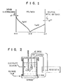
- Figure 1 is a schematic diagram of fluxes under steady-state conditions, wherein U e (x) and U m (x) on the vertical axis are position-dependent electrochemical potentials for the electrons and metal ions, respectively, as functions of the transverse distance across the polymeric film on tte horizontal axis x.
- U e (x) and U m (x) on the vertical axis are position-dependent electrochemical potentials for the electrons and metal ions, respectively, as functions of the transverse distance across the polymeric film on tte horizontal axis x.
- the two fluxes are each related to the mobilities and concentrations of the two species at the respective interfaces and to the gradient of electrochemical potential that they experience: wherein [P - ] o is the concentration of educed polymer functional groups at the cathode interface. [K n+ ] is the solution concentration of metal ions and K g is the partition coefficient for sorption of these ions by the polymer. The latter will defend on the characteristics of the counterions as well. [P - ] o can be related to the applied potential. E. and the standard half-cell potential for the polymer. E°, according to the Nernst equation: wherein [P] is the total concentration of redox-active functional groups in the polymer.
- equations (2) and (3) can be simplified to: or, with equation (1):
- Equation (7) was found to give a good representation for the embodiment in which the polymer is polyimide (ODA/PMDA), the metal ion is Ag + and the electrolyte is tetramethylammonium hexafluorophosphate (TMAPF 6 ) only when the concentration of electrolyte exceeded that of the Ag + salt by five-fold or more.
- the potential gradients are complex functions, involving both concentration gradients (diffusion) and electric field gradients (migration). Consequently, the gradients may not be strictly linear with respect to x, and they will be dependent on the concentrations, mobilities and sorption coefficients of all other ions in the system.
- the polymer is permeable towards the metal ions, there may be observed a steady-state current corresponding to deposition of the metal at the interface between the cathode and the polymer.
- This can be referred to as the "solution litited" current density, I s , because its magnitude is determined by the composition at the polymer/solution interface. I may not be strictly proportional to [Mn + ] t but will always vary directly with it.
- the solution composition is held constant and the applied potential is adjusted to a value more negative than the reduction potential of the polymer. If the polymer is capable of supporting an electron flux equal in magnitude to the metal ion flux. then the steady-state current measured under these conditions will exceed the value of I s determined for the same polymer film with the same solution composition.
- the fluxes of metal ions and electrons are maintained constant during a substantial period of the process so as to generate an interlayer with the maximum achievable density of metal particles.
- the fluxes of metal ions and electrons are varied systematically during a substantial pericd of the process so as to generate an interlayer of controlled density, lower than the maximum achievable density.
- Polyamic acid having an n inh of 1.48 dl/g (average of n inh ranging from 1.3 to 1.7) was prepared from 4,4'-oxydianiline and pyromellitic dianhydride.
- a 12 wt. % solution of the polyamic acid in dry N,N-dimethylacetamide (DMAc) was filtered through a Milliporee (10.0 ⁇ m pore) filter. A clean.
- SnO 2 -coated glass plate was spin-coated with this solution using a Headway Research Inc. Model EC101D Photoresist Spinner at 1000 rpm. The plate was transferred to a hot plate at 80°C for a period of 10 minutes until the polymer formed a clear, colorless solid film.
- the film was converted to the polyimide structure by immersing the plate in a mixture of acetic anhydride and pyridine (equal parts by volume) for a period of two h at room temperature, by which time it acquired the typical yellow gold color of the polyimide but remained clear and adherent.
- the film was rinsed thoroughly with methanol and then air dried. Conversion to polyimide was confirmed by infrared analysis.
- the film thickness was determined using transmission electron microscopy (TEM) of microtomed cross-sections and found to be 2.17 ⁇ m.
- the metal ion deposition process can be carried out with either controlled potential or controlled current.
- the former requires a conventional three-electrode configuration and potentiostat: the latter does not require a reference electrode.
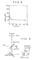
- Figure 2 depicts a typical apparatus for the electrochemical deposition of a silver interlayer in a polyimide film by means of the process of the invention.
- the cell consists of a Pyrex® cylinder sealed to the surface of the polymer-coated cathode by means of an 0-ring and clamp (not shown).
- the counter electrode and reference electrode are beth silver wires and they are connected along with the cathode to a potentiostat (Princeton Applied Research Model 173).
- the electrolyte solution is stirred and purged with a stream of nitrogen (not shown).
- the experiment was begun by adjusting the potential from +0.30 V (vs. an Ag wire reference electrode) to -1.30 V.
- the current measured as a function of time is shown in Figure 3.
- the experiment was terminated by opening the circuit when the total amount of charge passed reached 2.0 coulombs.
- the polymer film was then washed thoroughly with methanol. In appearance it was a bright gold-colored mirror when viewed from the side originally exposed to the solution and dark black when viewed through the glass cathode.
- the film was removed intact from the cathode by peeling it carefully away while immersed in aqueous methanol. It was allowed to dry at room temperature.
- TEM transmission electron microscopy
- the thickness of the metal interlayer formed under steady-state deposition conditions is proportional to the quantity of metal incorporated for a fixed surface area of polymer film. As judged by TEM of microtored thin sections, an interlayer of 5 0 0 A to 10.000 A can be produced within a precision of +250 A.
- Example 1 Nine polymer-coated cathodes were prepared and each was subjected to identical deposition conditions as in Example 1. The quantity of silver was controlled by opening the circuit after the desired amount of charge had been passed. The products were recovered and analyzed by TEM. Table 1 summarizes the results and Figure 4 shows the dependence of Ag interlayer thickness on the total Ag content of the sample. Silver contents were determined coulometrically.
- a linear least squares best fit to the data indicates that the silver interlayer is first established after approximately .04 mg/cm of deposition. This corresponds to the establishment of steady-state conditions as indicated, for example, by constancy of the current ( Figure 3).
- the linear dependence of t A g on Ag content demonstrates that, once formed, the interlayer grows in thickness at constant density.
- the density, calculated from the slope of the line, is 7.45 g Ag/cm . 71% of that for pure Ag.
- the process of the invention can be used to prepare mirrors.
- the reference mirror is a first surface mirror coated with a 3 ⁇ m ODA/PMDA polyimide film.
- the sample is a layer of silver electrodeposited into ODA/PMDA polyimide film. This choice of reference compensates for absorptive and scattering corrections which are introduced into the experiment by the polymer film.
- the intensity of light reflected by the sample is measured at its optimum orientation with respect to the laser beam and this is compared directly with the reading obtained from a reference first-surface mirror overcoated with polymer, located in a fixed position directly behind the sample holder.
- the ratio of the photosignal with the sample in the lower arm of the reflectometer to that reflected from the reference mirror yields reflectivity R of the silver layer.
- Table 2 shows reflectivities (R, in %) for samples with different silver loadings. The conductivity o was estimated from the reflectivity R at the laser frequency v and is shown in the table.
- the sheet resistance was measured using the "four-point probe" technique of Berry, Hall and Harris, supra. In this method, four contacts are made to the film; current is injected across the outer pair of contacts, and the resultant voltage drop across the two remaining points is measured.
- the sheet iesistance (R s ) of a layer of thickness t A g is proportional to the ratio of the voltage (V) to the current (I).
- the conductive interlayer resides beneath the external surfaces of the polymer. Consequently, only very high resistances were measured for contacts placed on these surfaces. Electrical characterizations of the interlayers per se were made by creating holes in the film at the desired contact positions and filling these holes with solder or conductive paste. The constant C was measured using thin sputtered gold layers of known specific conductivity and thickness d.
- the temperature coefficient of resistance (TCR) is defined as (1/R) (dR/dT).
- dR/dT is essentially independent of temperature and wherein R rt is the resistance at room temperature (T rt ), and R 1 is the resistance at some other temperature (T 1 ).
- the measurements herein were carried out between liquid nitrogen temperature (-196°C) and 22°C.
- the specific conductivity and TCR values of the interlayers are tabulated in Table 3.
- Figure 8 is a photomicrograph of a typical silver interlayer deposited in a polyimide film by means of the process of the invention, the film being microtomed in cross section and viewed in transmission.
- the reference marker represents l ⁇ (10,000 A).
- the silver interlayer thickness is approximately 3,800 A and the film thickness is approximately 92,000 A. Adjacent the interlayer are isolated silver particles. While carrying out the process of the invention the lower right surface of the film was on the cathode, the upper left surface was in contact with the metal ion source.
- a polymer-coated cathode was prepared by the procedure described in Example 1 using as the cathode a chromium-on-glass commercial photomask (Photographic Sciences Corp., USAF 1951 test chart, MT-14). This mask includes bars and spaces in a chromium layer where the rinimum features are 2.2 microns wide.
- Metal interlayer deposition was carried out with 0.01 M AgBF 4 in DAF without electrolyte. The current was maintained at 0.11 mA/cm 2 until .21 coulomb/cm 2 had been deposited. The current was turned off, the film was washed with methanol and removed from the surface of the cathode. The pattern of the original cathode was reproduced as a silver mirror within the polymer film. In particular, the 2.2 micron bars and spaces were reproduced in the interlayer. The original chromium image was in no way affected by the process and could be used again to repeat the process with a new polymeric film.
- Example 1 employed as the cathode and was prepared as described in Example 1.
- a photoresist layer KTI negative resist
- This layer was cured at 90°C for 10 minutes and then exposed under a test image photomask comprising bars and lines.
- the photoresist was developed by employing conditions recommended by the manufacturer.
- a silver interlayer was deposited using a solution 0.10 M in TMAPF 6 , 0.01 M in AgBF 4 and a constant potential of -1.30 V vs. Ag/Ag + .
- the silver interlayer became visible and developed only in those regions of the sample where development had removed the photoresist from the surface.
- the process was stopped after .07 coulomb/cm 2 had been deposited; the sample was washed with methanol and inspected under an optical microscope.
- the interlayer appeared as a reflective image which faithfully reproduced the image recorded in the photoresist mask.
- a copper interlayer was deposited into a film of ODA/PMDA polyimide coated onto a glass cathode coated with SnO 2 , prepared as in Example 1. Deposition was carried out using 0.10 M TNAPF 6 and 0.0 2 M Cu(AN) 4 PF 6 in DMF, wherein AN is acetonitrile. The potential was maintained at -1.30 V vs. Ag/Ag + and 0.18 coulomb/cm 2 was deposited. The film was washed with methanol, removed from the cathode and examined as a microtomed cross-section by TEM. The copper metal was observed as polyhedral particles, roughly 500 A in diameter, in a tightly distributed band 0.4 micron wide at a depth d/t of 0.85.
- a polyimide-coated, SnO 2 -coated glass cathode was prepared as in Example 1.
- the cathode was mounted in the cell which was filled with 0.10 M TMAPF 6 and 0.002 M AgBF 4 in DMF.
- Deposition was carried out employing an applied potential which was continuously varied between -0.90 and -1.30 V vs. Ag/Ag + .
- the potential was programmed in a "saw tooth" manner, i.e., it was changed linearly with time between the two limits at a rate of 10 mV per second. Deposition was continued until the total silver content reached 0.16 mg/cm .
- FIG. 9 shows a transmission electron micrograph prepared from this product microtomed in cross-section. It is apparent that the silver microparticles are distributed as a broad interlayer approximately 1 ⁇ in thickness, corresponding to a volume fraction of silver of 18%, about one-fourth that obtained under steady-state conditions.
- the scale bar at the bottom represents 1.0 u.
- the polymer film, 7.8 u thick, is seen with the original cathode interface on the upper left and the original metal ion solution interface on the lower right.
- the dark line at the solution interface is a Au/Pd film applied evaporatively prior to microtoming the sample.
- Example 1 The best mode presently contemplated for carrying out the invention is illustrated by Example 1.
Landscapes
- Chemical & Material Sciences (AREA)
- Chemical Kinetics & Catalysis (AREA)
- Engineering & Computer Science (AREA)
- Materials Engineering (AREA)
- Metallurgy (AREA)
- Organic Chemistry (AREA)
- Mechanical Engineering (AREA)
- Electrochemistry (AREA)
- Macromolecular Compounds Obtained By Forming Nitrogen-Containing Linkages In General (AREA)
- Laminated Bodies (AREA)
- Electroplating Methods And Accessories (AREA)
- Compositions Of Macromolecular Compounds (AREA)
Applications Claiming Priority (2)
| Application Number | Priority Date | Filing Date | Title |
|---|---|---|---|
| US06/633,502 US4512855A (en) | 1984-07-23 | 1984-07-23 | Deposition of metals as interlayers within organic polymeric films |
| US633502 | 1984-07-23 |
Publications (2)
| Publication Number | Publication Date |
|---|---|
| EP0169312A1 true EP0169312A1 (de) | 1986-01-29 |
| EP0169312B1 EP0169312B1 (de) | 1989-09-27 |
Family
ID=24539881
Family Applications (1)
| Application Number | Title | Priority Date | Filing Date |
|---|---|---|---|
| EP19850104688 Expired EP0169312B1 (de) | 1984-07-23 | 1985-04-18 | Abscheidung von Metallen als Zwischenschichten innerhalb von Filmen organischer Polymere |
Country Status (7)
| Country | Link |
|---|---|
| US (1) | US4512855A (de) |
| EP (1) | EP0169312B1 (de) |
| JP (1) | JPS6130698A (de) |
| AU (2) | AU4280485A (de) |
| BR (1) | BR8503262A (de) |
| CA (1) | CA1247036A (de) |
| DE (1) | DE3573279D1 (de) |
Cited By (3)
| Publication number | Priority date | Publication date | Assignee | Title |
|---|---|---|---|---|
| USRE45141E1 (en) | 2001-12-28 | 2014-09-23 | Trisa Holding Ag | Toothbrush and process for producing such a toothbrush |
| US10405642B2 (en) | 2002-12-19 | 2019-09-10 | Trisa Holding Ag | Toothbrush and process for producing the same |
| US11219303B2 (en) | 2016-04-20 | 2022-01-11 | Trisa Holding Ag | Brush product and method for the production thereof |
Families Citing this family (28)
| Publication number | Priority date | Publication date | Assignee | Title |
|---|---|---|---|---|
| EP0160558B1 (de) * | 1984-04-30 | 1991-07-17 | Nitto Denko Corporation | Polyimid-Zusammensetzung zum Verkleben metallischer Folien |
| US4692387A (en) * | 1984-10-02 | 1987-09-08 | E. I. Du Pont De Nemours And Company | Sintering of metal interlayers within organic polymeric films |
| DE3585715D1 (de) * | 1984-10-02 | 1992-04-30 | Du Pont | Sintern von metallischen zwischenschichten in organischen polymerfilmen. |
| US4752529A (en) * | 1986-01-21 | 1988-06-21 | E. I. Du Pont De Nemours And Company | Metal interlayers in films by counter-current diffusion |
| US4692360A (en) * | 1986-01-21 | 1987-09-08 | E. I. Du Pont De Nemours And Company | Metal interlayers in films by counter-current diffusion |
| US4657833A (en) * | 1986-02-11 | 1987-04-14 | E. I. Du Pont De Nemours And Company | Photosensitive cathode for deposition of metal structures within organic polymeric films |
| US4710403A (en) * | 1986-05-05 | 1987-12-01 | Minnesota Mining And Manufacturing Company | Metallized polymers |
| US4775556A (en) * | 1986-08-05 | 1988-10-04 | Minnesota Mining And Manufacturing Company | Process for metallized imaging |
| US4830903A (en) * | 1986-08-29 | 1989-05-16 | E. I. Du Pont De Nemours And Company | Catalytic deposition of metals in solid matrices |
| US4668354A (en) * | 1986-08-29 | 1987-05-26 | E. I. Du Pont De Nemours And Company | Electrocatalytic deposition of metals in solid polymeric matrices |
| US4774157A (en) * | 1987-05-19 | 1988-09-27 | E. I. Du Pont De Nemours And Company | Patterned metal interlayer in a matrix |
| JP2532589B2 (ja) * | 1988-06-29 | 1996-09-11 | 松下電器産業株式会社 | 微細パタ―ン形成方法 |
| US5242713A (en) * | 1988-12-23 | 1993-09-07 | International Business Machines Corporation | Method for conditioning an organic polymeric material |
| US5489370A (en) * | 1989-05-08 | 1996-02-06 | Ionex | Removal of ions from a bulk source by electropotential ion transport using a host receptor matrix |
| US5405509A (en) * | 1989-05-08 | 1995-04-11 | Ionex | Remediation of a bulk source by electropotential ion transport using a host receptor matrix |
| US5104944A (en) * | 1989-07-18 | 1992-04-14 | International Business Machines Corporation | Process for nucleophilic derivatization of materials having an imide group conjugated to an aromatic moiety |
| US5045159A (en) * | 1989-07-18 | 1991-09-03 | International Business Machines Corporation | Derivatives of compounds containing a carbonyl group conjugated to an aromatic moiety and electrophilic methods of fabrication thereof |
| US5015538A (en) * | 1989-09-22 | 1991-05-14 | Minnesota Mining And Manufacturing Company | Process for pulse electroplating electroactive polymers and articles derived therefrom |
| US5021129A (en) * | 1989-09-25 | 1991-06-04 | International Business Machines Corporation | Multilayer structures of different electroactive materials and methods of fabrication thereof |
| JP2524436B2 (ja) * | 1990-09-18 | 1996-08-14 | インターナショナル・ビジネス・マシーンズ・コーポレイション | 表面処理方法 |
| US5152880A (en) * | 1991-03-28 | 1992-10-06 | International Business Machines Corporation | Electrodeposition of a polymer |
| CA2051604A1 (fr) * | 1991-09-17 | 1993-03-18 | Guy St-Amant | Feuillards metalliques supportes sur plastique obtenu par metallisation-placage |
| US5677418A (en) * | 1995-06-14 | 1997-10-14 | The United States Of America As Represented By The Administrator Of The National Aeronautics And Space Administration | Reflective self-metallizing polyimide films |
| US6203758B1 (en) * | 1997-11-10 | 2001-03-20 | Bio-Pixel Ltd. | Micro-circuit system with array of functionalized micro-electrodes |
| JP3065041B2 (ja) * | 1998-10-29 | 2000-07-12 | アプライド マテリアルズ インコーポレイテッド | 半導体デバイスの成膜方法及び成膜装置 |
| US6440711B1 (en) | 2000-12-08 | 2002-08-27 | Board Of Trustees Southern Illinois University, The | Dehydrogenase enzymatic synthesis of methanol |
| TWI297513B (en) * | 2005-10-06 | 2008-06-01 | Ind Tech Res Inst | Electrode and method for forming the same |
| US7955662B2 (en) * | 2006-09-29 | 2011-06-07 | The University Of Tokyo | Optical multilayer reflective film, and aligned metal particle film and manufacturing process therefor |
Citations (4)
| Publication number | Priority date | Publication date | Assignee | Title |
|---|---|---|---|---|
| US3407125A (en) * | 1965-01-18 | 1968-10-22 | Corning Glass Works | Method of making filamentary metal structures |
| DE1571747B2 (de) * | 1965-09-30 | 1977-03-10 | Leesona Corp., Warwick, RJ. (V.StA.) | Mehrschicht-gasdiffusionselektrode fuer brennstoffelemente |
| DE2811151B2 (de) * | 1978-03-15 | 1980-10-09 | Flachglas Ag, 8510 Fuerth | Verfahren zum Herstellen eines mehrschichtigen Verbundkörpers |
| DE3324968A1 (de) * | 1982-07-12 | 1984-01-12 | Nippondenso Co., Ltd., Kariya, Aichi | Verfahren zur bildung einer elektrode eines organischen elements |
Family Cites Families (2)
| Publication number | Priority date | Publication date | Assignee | Title |
|---|---|---|---|---|
| US3549505A (en) * | 1967-01-09 | 1970-12-22 | Helmut G Hanusa | Reticular structures and methods of producing same |
| IL67556A (en) * | 1981-12-28 | 1987-10-20 | Chevron Res | Batteries fabricated with electroactive polymers |
-
1984
- 1984-07-23 US US06/633,502 patent/US4512855A/en not_active Expired - Fee Related
-
1985
- 1985-04-02 CA CA000478167A patent/CA1247036A/en not_active Expired
- 1985-04-11 JP JP7548885A patent/JPS6130698A/ja active Pending
- 1985-04-18 DE DE8585104688T patent/DE3573279D1/de not_active Expired
- 1985-04-18 EP EP19850104688 patent/EP0169312B1/de not_active Expired
- 1985-05-23 AU AU42804/85A patent/AU4280485A/en not_active Abandoned
- 1985-07-08 BR BR8503262A patent/BR8503262A/pt not_active IP Right Cessation
-
1989
- 1989-10-12 AU AU42801/89A patent/AU4280189A/en not_active Abandoned
Patent Citations (4)
| Publication number | Priority date | Publication date | Assignee | Title |
|---|---|---|---|---|
| US3407125A (en) * | 1965-01-18 | 1968-10-22 | Corning Glass Works | Method of making filamentary metal structures |
| DE1571747B2 (de) * | 1965-09-30 | 1977-03-10 | Leesona Corp., Warwick, RJ. (V.StA.) | Mehrschicht-gasdiffusionselektrode fuer brennstoffelemente |
| DE2811151B2 (de) * | 1978-03-15 | 1980-10-09 | Flachglas Ag, 8510 Fuerth | Verfahren zum Herstellen eines mehrschichtigen Verbundkörpers |
| DE3324968A1 (de) * | 1982-07-12 | 1984-01-12 | Nippondenso Co., Ltd., Kariya, Aichi | Verfahren zur bildung einer elektrode eines organischen elements |
Cited By (4)
| Publication number | Priority date | Publication date | Assignee | Title |
|---|---|---|---|---|
| USRE45141E1 (en) | 2001-12-28 | 2014-09-23 | Trisa Holding Ag | Toothbrush and process for producing such a toothbrush |
| USRE47468E1 (en) | 2001-12-28 | 2019-07-02 | Trisa Holding Ag | Toothbrush and process for producing such a toothbrush |
| US10405642B2 (en) | 2002-12-19 | 2019-09-10 | Trisa Holding Ag | Toothbrush and process for producing the same |
| US11219303B2 (en) | 2016-04-20 | 2022-01-11 | Trisa Holding Ag | Brush product and method for the production thereof |
Also Published As
| Publication number | Publication date |
|---|---|
| BR8503262A (pt) | 1986-04-01 |
| JPS6130698A (ja) | 1986-02-12 |
| AU4280485A (en) | 1986-01-30 |
| DE3573279D1 (en) | 1989-11-02 |
| AU4280189A (en) | 1990-02-15 |
| US4512855A (en) | 1985-04-23 |
| CA1247036A (en) | 1988-12-20 |
| EP0169312B1 (de) | 1989-09-27 |
Similar Documents
| Publication | Publication Date | Title |
|---|---|---|
| EP0169312B1 (de) | Abscheidung von Metallen als Zwischenschichten innerhalb von Filmen organischer Polymere | |
| EP2849265B1 (de) | Lithium-Ionen-Batterie | |
| EP0419804B1 (de) | Mehrschichtige Strukturen aus verschiedenen elektroaktiven Materialien sowie Verfahren zur deren Herstellung | |
| KR101117552B1 (ko) | 휘스커 형성 경향이 적은 주석 코팅된 인쇄회로기판 | |
| DE69705593T2 (de) | Verfahren zur erzeugung von passiven bauelementen unter verwendung von leitenden polypyrrolzusammensetzungen | |
| Mazur et al. | Electrochemical growth of metal interlayers in polyimide film | |
| EP2820657A1 (de) | Leitende nanodrahtfilme | |
| Harsanyi | Irregular effect of chloride impurities on migration failure reliability: contradictions or understandable? | |
| KR900005138B1 (ko) | 고형 매트릭스내의 금속 촉매 용착 방법 | |
| US4692387A (en) | Sintering of metal interlayers within organic polymeric films | |
| Cui et al. | The evolution of Pd∕ Sn catalytic surfaces in electroless copper deposition | |
| US4692360A (en) | Metal interlayers in films by counter-current diffusion | |
| US5158657A (en) | Circuit substrate and process for its production | |
| US4879270A (en) | Method of forming superconducting ceramics by electrodeposition | |
| US4830903A (en) | Catalytic deposition of metals in solid matrices | |
| EP0423190B1 (de) | Metallisierte polymere und verfahren | |
| EP0177012B1 (de) | Sintern von metallischen Zwischenschichten in organischen Polymerfilmen | |
| Minì et al. | Copper patterning on dielectrics by laser writing in liquid solution | |
| JPH01201486A (ja) | 耐マイグレーション性に優れた導電塗料用Agめっき複合粉末 | |
| US4752529A (en) | Metal interlayers in films by counter-current diffusion | |
| Balakrishnan et al. | Electrodeposition technique and properties of semiconducting cadmium chalcogenide thin films from aprotic electrolytes | |
| Soga et al. | Preparation and electrical conductivity of thin films of Rb4Cu16I7Cl13 | |
| WO1989010336A1 (en) | Superconducting ceramics by electrodeposition | |
| Ng et al. | Effect of crystallographic orientation on contact resistance of electroplated nickel alloys | |
| Mazur et al. | Metal Interlayers in Polymer Films: A Survey of Deposition Processes, Morphology, Patterning Methods and Physical Properties |
Legal Events
| Date | Code | Title | Description |
|---|---|---|---|
| PUAI | Public reference made under article 153(3) epc to a published international application that has entered the european phase |
Free format text: ORIGINAL CODE: 0009012 |
|
| AK | Designated contracting states |
Designated state(s): BE DE FR GB IT NL |
|
| 17P | Request for examination filed |
Effective date: 19860728 |
|
| 17Q | First examination report despatched |
Effective date: 19870805 |
|
| GRAA | (expected) grant |
Free format text: ORIGINAL CODE: 0009210 |
|
| AK | Designated contracting states |
Kind code of ref document: B1 Designated state(s): BE DE FR GB IT NL |
|
| ITF | It: translation for a ep patent filed | ||
| REF | Corresponds to: |
Ref document number: 3573279 Country of ref document: DE Date of ref document: 19891102 |
|
| ET | Fr: translation filed | ||
| PLBE | No opposition filed within time limit |
Free format text: ORIGINAL CODE: 0009261 |
|
| STAA | Information on the status of an ep patent application or granted ep patent |
Free format text: STATUS: NO OPPOSITION FILED WITHIN TIME LIMIT |
|
| 26N | No opposition filed | ||
| PGFP | Annual fee paid to national office [announced via postgrant information from national office to epo] |
Ref country code: BE Payment date: 19910326 Year of fee payment: 7 |
|
| ITTA | It: last paid annual fee | ||
| PG25 | Lapsed in a contracting state [announced via postgrant information from national office to epo] |
Ref country code: BE Effective date: 19920430 |
|
| BERE | Be: lapsed |
Owner name: E.I. DU PONT DE NEMOURS AND CY Effective date: 19920430 |
|
| PGFP | Annual fee paid to national office [announced via postgrant information from national office to epo] |
Ref country code: FR Payment date: 19930226 Year of fee payment: 9 |
|
| PGFP | Annual fee paid to national office [announced via postgrant information from national office to epo] |
Ref country code: GB Payment date: 19930329 Year of fee payment: 9 |
|
| PGFP | Annual fee paid to national office [announced via postgrant information from national office to epo] |
Ref country code: DE Payment date: 19930419 Year of fee payment: 9 |
|
| PGFP | Annual fee paid to national office [announced via postgrant information from national office to epo] |
Ref country code: NL Payment date: 19930430 Year of fee payment: 9 |
|
| PG25 | Lapsed in a contracting state [announced via postgrant information from national office to epo] |
Ref country code: GB Effective date: 19940418 |
|
| PG25 | Lapsed in a contracting state [announced via postgrant information from national office to epo] |
Ref country code: NL Effective date: 19941101 |
|
| GBPC | Gb: european patent ceased through non-payment of renewal fee |
Effective date: 19940418 |
|
| NLV4 | Nl: lapsed or anulled due to non-payment of the annual fee | ||
| PG25 | Lapsed in a contracting state [announced via postgrant information from national office to epo] |
Ref country code: FR Effective date: 19941229 |
|
| PG25 | Lapsed in a contracting state [announced via postgrant information from national office to epo] |
Ref country code: DE Effective date: 19950103 |
|
| REG | Reference to a national code |
Ref country code: FR Ref legal event code: ST |