EP0169351A2 - Réseau de portes intégrées sur une puce - Google Patents
Réseau de portes intégrées sur une puce Download PDFInfo
- Publication number
- EP0169351A2 EP0169351A2 EP85106816A EP85106816A EP0169351A2 EP 0169351 A2 EP0169351 A2 EP 0169351A2 EP 85106816 A EP85106816 A EP 85106816A EP 85106816 A EP85106816 A EP 85106816A EP 0169351 A2 EP0169351 A2 EP 0169351A2
- Authority
- EP
- European Patent Office
- Prior art keywords
- transistor
- data
- word
- circuit
- collector
- Prior art date
- Legal status (The legal status is an assumption and is not a legal conclusion. Google has not performed a legal analysis and makes no representation as to the accuracy of the status listed.)
- Withdrawn
Links
Images


Classifications
-
- H—ELECTRICITY
- H03—ELECTRONIC CIRCUITRY
- H03K—PULSE TECHNIQUE
- H03K3/00—Circuits for generating electric pulses; Monostable, bistable or multistable circuits
- H03K3/02—Generators characterised by the type of circuit or by the means used for producing pulses
- H03K3/26—Generators characterised by the type of circuit or by the means used for producing pulses by the use, as active elements, of bipolar transistors with internal or external positive feedback
- H03K3/28—Generators characterised by the type of circuit or by the means used for producing pulses by the use, as active elements, of bipolar transistors with internal or external positive feedback using means other than a transformer for feedback
- H03K3/281—Generators characterised by the type of circuit or by the means used for producing pulses by the use, as active elements, of bipolar transistors with internal or external positive feedback using means other than a transformer for feedback using at least two transistors so coupled that the input of one is derived from the output of another, e.g. multivibrator
- H03K3/286—Generators characterised by the type of circuit or by the means used for producing pulses by the use, as active elements, of bipolar transistors with internal or external positive feedback using means other than a transformer for feedback using at least two transistors so coupled that the input of one is derived from the output of another, e.g. multivibrator bistable
- H03K3/288—Generators characterised by the type of circuit or by the means used for producing pulses by the use, as active elements, of bipolar transistors with internal or external positive feedback using means other than a transformer for feedback using at least two transistors so coupled that the input of one is derived from the output of another, e.g. multivibrator bistable using additional transistors in the input circuit
-
- G—PHYSICS
- G11—INFORMATION STORAGE
- G11C—STATIC STORES
- G11C11/00—Digital stores characterised by the use of particular electric or magnetic storage elements; Storage elements therefor
- G11C11/21—Digital stores characterised by the use of particular electric or magnetic storage elements; Storage elements therefor using electric elements
- G11C11/34—Digital stores characterised by the use of particular electric or magnetic storage elements; Storage elements therefor using electric elements using semiconductor devices
- G11C11/40—Digital stores characterised by the use of particular electric or magnetic storage elements; Storage elements therefor using electric elements using semiconductor devices using transistors
- G11C11/41—Digital stores characterised by the use of particular electric or magnetic storage elements; Storage elements therefor using electric elements using semiconductor devices using transistors forming static cells with positive feedback, i.e. cells not needing refreshing or charge regeneration, e.g. bistable multivibrator or Schmitt trigger
- G11C11/411—Digital stores characterised by the use of particular electric or magnetic storage elements; Storage elements therefor using electric elements using semiconductor devices using transistors forming static cells with positive feedback, i.e. cells not needing refreshing or charge regeneration, e.g. bistable multivibrator or Schmitt trigger using bipolar transistors only
- G11C11/4116—Digital stores characterised by the use of particular electric or magnetic storage elements; Storage elements therefor using electric elements using semiconductor devices using transistors forming static cells with positive feedback, i.e. cells not needing refreshing or charge regeneration, e.g. bistable multivibrator or Schmitt trigger using bipolar transistors only with at least one cell access via separately connected emittors of said transistors or via multiple emittors, e.g. T2L, ECL
-
- H—ELECTRICITY
- H10—SEMICONDUCTOR DEVICES; ELECTRIC SOLID-STATE DEVICES NOT OTHERWISE PROVIDED FOR
- H10D—INORGANIC ELECTRIC SEMICONDUCTOR DEVICES
- H10D84/00—Integrated devices formed in or on semiconductor substrates that comprise only semiconducting layers, e.g. on Si wafers or on GaAs-on-Si wafers
- H10D84/90—Masterslice integrated circuits
- H10D84/901—Masterslice integrated circuits comprising bipolar technology
Definitions
- This invention relates generally to integrated circuits. More particularly this invention relates to an improved gate array chip for fabricating logic and array(s) on the same chip.
- VLSI VLSI it is desirable to incorporate logic and a memory array (or arrays) on the same chip. To do this efficiently over a wide range of application, flexibility of organization is required.
- the disclosed invention facilitates the mixing of logic and array(s) on the same chip.
- the memory cell is D.C. testable.
- the first approach is to replace a portion of the logic silicon with array silicon. It has the characteristic of requiring a standard A.C. testing.
- a second approach is to personalize the logic devices to form a standard array circuit. This would require unembedding the array (making it available at I/O's) and A.C. testing it (thus increasing cost).
- the invention as claimed is intended to remedy these drawbacks. It solves the problem of how to design an integrated circuit chip wherein logic and memory array(s) are efficiently and effectively integrated for functional use and as well as initial testing.
- a further object of the invention is to provide an integrated circuit chip containing p thousand (where p is a positive integer) identical cell, each cell containing components such transistors, resistor diodes, etc.
- the metallization of only a single cell is required to provide a multi-input TTL logic circuit or a single binary bit memory cell for use in a chip containing a memory array and logic circuitry or the like.
- the invention discloses and utilizes a basic memory cell circuit designed for an array to mix with logic.
- a primary advantage is that it is DC testable. Therefor it can be treated as a standard logic macro.
- the gate array user may design any size and organization that is needed. It also can allow for more than one array on chip.
- the design is set up to use the opposite philosophy than normal RAM designs, instead of trying to minimize the signal swing, they have been increased to look like normal internal circuit levels.
- the first approach is to replace a portion of the Gate Array with a Custom Designed RAM - a hybrid approach.
- Such designs traditionally tend to utilize the process to its fullest.
- the circuit designs tend to have small signal swings to increase the RAM's access time, resulting in a design with lower noise margin than its logic counterpart.
- the net result is a RAM that is more sensitive to process variations than the logic. This sensitivity manifests itself in the defective product failing under rather extraordinary circumstances.
- One such failure mode is called a disturb.
- a disturb is an unintentioned change of state of the memory. This failure can occur under a variety of differing circumstances - varying the RAM patterns or modifying the timings applied to the memory.
- Such tests are usually voluminous in nature and applied to the ARRAY at or near the cycle time of the product.
- Figure 1 illustrates a basic RAM cell that can be used as a standard logic macro, defined through personalization of a Gate Array.
- the cell is fed by standard TTL gates, and its fanout is equivalent to that of a standard design - 1 to 8 approximately.
- This cell differs from other cell designs in its inherent stability, its freedom from hazards, and its comparable noise margin to that of logic.
- the basic memory cell circuit ( Figure 1) designed for an array to mix with logic comprises word read circuit means having at least one word read line, word write circuit means having at least one word write line, data In circuit means having at least one data In bit line, and data Out circuit means having at least one data Out bit line.
- first and second transistors TlA, TlB are connected in common to said data In bit line, the emitter of a third transistor TIC is connected to said word write line, the emitter of a fourth transistor T2 being connected to a second source of potential.
- the collector of a fifth transistor T3 is connected to said data Out bit line.
- a first resistor Rl is connected between the base of said first transistor T1A and said word write line.
- a second resistor R2 is connected between a common connection of the collector of said first transistor T1A, the collector of said second transistor T1B, the collector of said third transistor TIC, and the base of said fourth transistor T2 and a first source of potential V.
- a third resistor R3 is connected between a common connection of the base of said second transistor T1B, the base of said third transistor TIC, the collector of said fourth transistor T2 and the emitter of said fifth transistor T3 and said first source of potential V.
- a fourth resistor R4 is connected between the base of said fifth transistor T3 and said word read line, said first, second and third transistors TlA, T IB, TIC are provided by a single integrated circuit semiconductor transistor structure having a collector region for providing in common the collectors of said first, second and third transistors, a first base region for providing the base of said first transistor, a second base region for providing in common the base of said second and third transistors, and first, second and third emitters for respectively providing said emitters of said first, second and third transistors.
- a first Schottky diode Dl is connected across the collector-base junction of the first transistor T1A
- a second Schottky diode D2 is connected across the common collector-base junction of the second and third transistors TIB, TIC
- a third Schottky diode D3 is connected across the collector-base junction of the fourth transistor T2
- a fourth Schottky diode D4 is connected across the common collector-base junction of the fifth transistor T3.
- the word write line is high turning TIC Off.
- the combination of T1A, T2, R1, R2 and R3 are utilized to set new data into the latch or memory cell.
- the word write line is Down and TIA is turned Off.
- TIC, T2 form an internal circuit and data is maintained in the latch.
- D.C. testability is demonstrated by the fact that these operating regions are identical to the conventional logic circuits. Therefore they have the same propensity for noise rejection.
- a further consideration is the transition from "write" to "hold”. As the word write line is dropped T1A can turn off faster than TIC turns on (especially true with slow rise time card testers). This could cause a problem if negative data is being stored.
- TIB solves this problem by holding the collector of Tl down until T1C is turned on. Thus of course, that Data has to remain valid until the word write line has been removed.
- T1A is on the collector of Tl is pulled low, otherwise R2 will pull the collector high.
- the T2 device is used to bias the base of T1C and TIB.
- T2 is off and therefore the base of TIC and T1B is high.
- TIA turns off before T1C turns on to hold the base of T2 low.
- This race condition is termed a hazard.
- T1B is used to hold the base of T2 low during the transition of the Word Write Line to free the design from this hazard - thus a hazard-free latch design. This aspect of the design is important if our objective is to test the RAM as the industry tests logic.
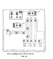
- FIG. 3 The Sense Amplifier for this design is shown in Figure 3.
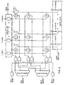
- Figure 4 depicts how the RAM cell and its Sense Amplifier are connected in order to configure a RAM.
- T3 of the basic cell, T4 within the Sense Amplifier are configured in a manner similar to the transistor configuration of a TTL gate in Figure 2.
- the Word Read Line, the Data-In Bit Line, and the Word Write Line are fed by regular TTL logic gates, an example of which is shown in Figure 2. From the basic memory cell's perspective, a read and write operation are logically divorced from one another. It is the logical configuration which feeds the memory cells which determine the relationship between reading and writing.
- a selected Word within the RAM may be both Written and Read simultaneously if both the Read Strobe and the Write Strobe are both active.
- the RAM configuration in Figure 5 using the same cell, has the option of two different addresses to the RAM selecting a different word for reading and writing.
- the RAM of Figure 4 is composed of a decoder, a matrix of the memory cells, and the sense and drive amplifiers.
- the decoder selects a row or word of cells according to the address value.
- the cells within the word are selected to read, or write, or to both read and write ' simultaneously. This is accomplished by placing the proper polarity on the Read and Write strobe inputs.
- the Word Write line of the basic cell is controlled by the output of the decoder and the write strobe input.
- the word must be addressed and the Write strobe active in order for information on the drive amplifiers to be accepted or written into the word.
- the word read line of the basic cell is controlled by the decoder and the read strobe. In a similar manner the word must be selected by the address with the read strobe active in order for valid word data to appear on the output of the sense amplifiers.
- Figure 5 represents a two port RAM.
- two decoders are realized - one for reading and the other for writing.
- the RAM operates similar to the implementation in Figure 4 except that in Figure 5 the word selected by the Read Address is Read and the word selected by the Write Address is written. If the Read Address and Write Address of Figure 5 were always equal, then Figure 5 and Figure 4 would be logically identical.
Landscapes
- Engineering & Computer Science (AREA)
- Microelectronics & Electronic Packaging (AREA)
- Computer Hardware Design (AREA)
- Power Engineering (AREA)
- Static Random-Access Memory (AREA)
- Design And Manufacture Of Integrated Circuits (AREA)
- Semiconductor Memories (AREA)
Applications Claiming Priority (2)
| Application Number | Priority Date | Filing Date | Title |
|---|---|---|---|
| US625426 | 1984-06-28 | ||
| US06/625,426 US4613958A (en) | 1984-06-28 | 1984-06-28 | Gate array chip |
Publications (2)
| Publication Number | Publication Date |
|---|---|
| EP0169351A2 true EP0169351A2 (fr) | 1986-01-29 |
| EP0169351A3 EP0169351A3 (fr) | 1989-02-08 |
Family
ID=24506023
Family Applications (1)
| Application Number | Title | Priority Date | Filing Date |
|---|---|---|---|
| EP85106816A Withdrawn EP0169351A3 (fr) | 1984-06-28 | 1985-06-03 | Réseau de portes intégrées sur une puce |
Country Status (3)
| Country | Link |
|---|---|
| US (1) | US4613958A (fr) |
| EP (1) | EP0169351A3 (fr) |
| JP (1) | JPS6116097A (fr) |
Families Citing this family (9)
| Publication number | Priority date | Publication date | Assignee | Title |
|---|---|---|---|---|
| JPS62202537A (ja) * | 1986-02-19 | 1987-09-07 | Hitachi Ltd | 半導体集積回路装置 |
| US4922441A (en) * | 1987-01-19 | 1990-05-01 | Ricoh Company, Ltd. | Gate array device having a memory cell/interconnection region |
| JP2547615B2 (ja) * | 1988-06-16 | 1996-10-23 | 三菱電機株式会社 | 読出専用半導体記憶装置および半導体記憶装置 |
| JP2600304B2 (ja) * | 1988-06-30 | 1997-04-16 | 三菱電機株式会社 | 半導体記憶装置とこれを用いたデータパス |
| DE3886938T2 (de) * | 1988-10-28 | 1994-06-30 | Ibm | Reprogrammierbare logische Sicherung für logische Anordnungen, basierend auf einer 6-Elementen-SRAM-Zelle. |
| KR100431478B1 (ko) * | 1995-07-27 | 2004-08-25 | 텍사스 인스트루먼츠 인코포레이티드 | 고밀도2포트메모리셀 |
| US6061759A (en) * | 1996-02-09 | 2000-05-09 | Apex Semiconductor, Inc. | Hidden precharge pseudo cache DRAM |
| US6880056B2 (en) * | 2002-03-28 | 2005-04-12 | Hewlett-Packard Development, L.P. | Memory array and method with simultaneous read/write capability |
| US8276105B2 (en) * | 2009-09-18 | 2012-09-25 | International Business Machines Corporation | Automatic positioning of gate array circuits in an integrated circuit design |
Family Cites Families (10)
| Publication number | Priority date | Publication date | Assignee | Title |
|---|---|---|---|---|
| US3427598A (en) * | 1965-12-09 | 1969-02-11 | Fairchild Camera Instr Co | Emitter gated memory cell |
| GB1162109A (en) * | 1966-12-22 | 1969-08-20 | Ibm | Semi Conductor Data and Storage Devices and Data Stores Employing Such Devices |
| GB1127270A (en) * | 1967-09-05 | 1968-09-18 | Ibm | Data storage cell |
| US3617772A (en) * | 1969-07-09 | 1971-11-02 | Ibm | Sense amplifier/bit driver for a memory cell |
| US3618052A (en) * | 1969-12-05 | 1971-11-02 | Cogar Corp | Bistable memory with predetermined turn-on state |
| US3634833A (en) * | 1970-03-12 | 1972-01-11 | Texas Instruments Inc | Associative memory circuit |
| US3740730A (en) * | 1971-06-30 | 1973-06-19 | Ibm | Latchable decoder driver and memory array |
| US4057789A (en) * | 1974-06-19 | 1977-11-08 | International Business Machines Corporation | Reference voltage source for memory cells |
| US4007451A (en) * | 1975-05-30 | 1977-02-08 | International Business Machines Corporation | Method and circuit arrangement for operating a highly integrated monolithic information store |
| US4035784A (en) * | 1975-12-22 | 1977-07-12 | Fairchild Camera And Instrument Corporation | Asymmetrical memory cell arrangement |
-
1984
- 1984-06-28 US US06/625,426 patent/US4613958A/en not_active Expired - Lifetime
-
1985
- 1985-04-16 JP JP60079454A patent/JPS6116097A/ja active Pending
- 1985-06-03 EP EP85106816A patent/EP0169351A3/fr not_active Withdrawn
Non-Patent Citations (3)
| Title |
|---|
| IBM TECHNCIAL DISCLOSURE BULLETIN, vol. 26, no. 10B, March 1984, pages 5681-5682, New York, US; L.C.RITCHIE et al.: "Two-write, multi-read RAM cell" * |
| IBM TECHNICAL DISCLOSURE BULLETIN, vol. 21, no. 5, October 1978, pages 1888-1891, New York, US, R.T.DENNISON: "Universal array/logic cell" * |
| IBM TECHNICAL DISCLOSURE BULLETIN, vol. 26, no. 7B, December 1983, pages 3626-3627, New York, US; M.N.SHEN: "Multi-port RAM cell" * |
Also Published As
| Publication number | Publication date |
|---|---|
| EP0169351A3 (fr) | 1989-02-08 |
| JPS6116097A (ja) | 1986-01-24 |
| US4613958A (en) | 1986-09-23 |
Similar Documents
| Publication | Publication Date | Title |
|---|---|---|
| EP0660332B1 (fr) | Méthode et appareil pour emmagasiner un état indifférent dans une cellule de mémoire associative | |
| US6011726A (en) | Four device SRAM cell with single bitline | |
| US4775942A (en) | Seed and stitch approach to embedded arrays | |
| KR100207941B1 (ko) | 공유 BiCMOS 감지 증폭기 | |
| US4817051A (en) | Expandable multi-port random access memory | |
| JPS619895A (ja) | 半導体記憶回路 | |
| JPH05166375A (ja) | 2重ポート式スタティック・ランダム・アクセス・メモリ・セル | |
| US5629943A (en) | Integrated circuit memory with double bitline low special test mode control from output enable | |
| EP0023792B1 (fr) | Mémoire à semi-conducteurs comprenant des cellules intégrées à injection logique | |
| US4613958A (en) | Gate array chip | |
| US4663741A (en) | Strobed access semiconductor memory system | |
| US6292388B1 (en) | Efficient and robust random access memory cell suitable for programmable logic configuration control | |
| US5748643A (en) | Fast scan GRA cell circuit | |
| US6418045B2 (en) | Efficient and robust random access memory cell suitable for programmable logic configuration control | |
| US4864539A (en) | Radiation hardened bipolar static RAM cell | |
| US4788662A (en) | Semiconductor memory device using resonant-tunneling hot electron transistor | |
| US5577051A (en) | Static memory long write test | |
| US4910711A (en) | Bicmos read/write control and sensing circuit | |
| EP0505652A1 (fr) | Système de stockage avec redondance adaptable | |
| US3820086A (en) | Read only memory(rom)superimposed on read/write memory(ram) | |
| US4280197A (en) | Multiple access store | |
| US5231345A (en) | Semiconductor integrated circuit device having a test circuit | |
| EP0020769B1 (fr) | Systeme de memoire a semi-conducteur | |
| KR100231966B1 (ko) | 정적 ram용 자동로킹 부하구조 | |
| EP0023408B1 (fr) | Mémoire à semi-conducteurs comprenant des cellules intégrées à injection logique |
Legal Events
| Date | Code | Title | Description |
|---|---|---|---|
| PUAI | Public reference made under article 153(3) epc to a published international application that has entered the european phase |
Free format text: ORIGINAL CODE: 0009012 |
|
| AK | Designated contracting states |
Designated state(s): DE FR GB |
|
| RIN1 | Information on inventor provided before grant (corrected) |
Inventor name: RITCHIE, LEONARD C. Inventor name: GRAF, MATTHEW CHRISTOPHER Inventor name: CULICAN, EDWARD FRANCIS |
|
| 17P | Request for examination filed |
Effective date: 19860424 |
|
| PUAL | Search report despatched |
Free format text: ORIGINAL CODE: 0009013 |
|
| AK | Designated contracting states |
Kind code of ref document: A3 Designated state(s): DE FR GB |
|
| 17Q | First examination report despatched |
Effective date: 19900426 |
|
| STAA | Information on the status of an ep patent application or granted ep patent |
Free format text: STATUS: THE APPLICATION IS DEEMED TO BE WITHDRAWN |
|
| 18D | Application deemed to be withdrawn |
Effective date: 19900907 |
|
| RIN1 | Information on inventor provided before grant (corrected) |
Inventor name: CULICAN, EDWARD FRANCIS Inventor name: RITCHIE, LEONARD C. Inventor name: GRAF, MATTHEW CHRISTOPHER |