EP0169518A2 - Flüssigkristallvorrichtung - Google Patents
Flüssigkristallvorrichtung Download PDFInfo
- Publication number
- EP0169518A2 EP0169518A2 EP85109091A EP85109091A EP0169518A2 EP 0169518 A2 EP0169518 A2 EP 0169518A2 EP 85109091 A EP85109091 A EP 85109091A EP 85109091 A EP85109091 A EP 85109091A EP 0169518 A2 EP0169518 A2 EP 0169518A2
- Authority
- EP
- European Patent Office
- Prior art keywords
- liquid crystal
- electrodes
- crystal composition
- electric field
- electrode
- Prior art date
- Legal status (The legal status is an assumption and is not a legal conclusion. Google has not performed a legal analysis and makes no representation as to the accuracy of the status listed.)
- Granted
Links
Images




Classifications
-
- G—PHYSICS
- G06—COMPUTING OR CALCULATING; COUNTING
- G06K—GRAPHICAL DATA READING; PRESENTATION OF DATA; RECORD CARRIERS; HANDLING RECORD CARRIERS
- G06K15/00—Arrangements for producing a permanent visual presentation of the output data, e.g. computer output printers
- G06K15/02—Arrangements for producing a permanent visual presentation of the output data, e.g. computer output printers using printers
- G06K15/12—Arrangements for producing a permanent visual presentation of the output data, e.g. computer output printers using printers by photographic printing, e.g. by laser printers
- G06K15/1238—Arrangements for producing a permanent visual presentation of the output data, e.g. computer output printers using printers by photographic printing, e.g. by laser printers simultaneously exposing more than one point
- G06K15/1242—Arrangements for producing a permanent visual presentation of the output data, e.g. computer output printers using printers by photographic printing, e.g. by laser printers simultaneously exposing more than one point on one main scanning line
- G06K15/1252—Arrangements for producing a permanent visual presentation of the output data, e.g. computer output printers using printers by photographic printing, e.g. by laser printers simultaneously exposing more than one point on one main scanning line using an array of light modulators, e.g. a linear array
-
- G—PHYSICS
- G02—OPTICS
- G02F—OPTICAL DEVICES OR ARRANGEMENTS FOR THE CONTROL OF LIGHT BY MODIFICATION OF THE OPTICAL PROPERTIES OF THE MEDIA OF THE ELEMENTS INVOLVED THEREIN; NON-LINEAR OPTICS; FREQUENCY-CHANGING OF LIGHT; OPTICAL LOGIC ELEMENTS; OPTICAL ANALOGUE/DIGITAL CONVERTERS
- G02F1/00—Devices or arrangements for the control of the intensity, colour, phase, polarisation or direction of light arriving from an independent light source, e.g. switching, gating or modulating; Non-linear optics
- G02F1/01—Devices or arrangements for the control of the intensity, colour, phase, polarisation or direction of light arriving from an independent light source, e.g. switching, gating or modulating; Non-linear optics for the control of the intensity, phase, polarisation or colour
- G02F1/13—Devices or arrangements for the control of the intensity, colour, phase, polarisation or direction of light arriving from an independent light source, e.g. switching, gating or modulating; Non-linear optics for the control of the intensity, phase, polarisation or colour based on liquid crystals, e.g. single liquid crystal display cells
- G02F1/133—Constructional arrangements; Operation of liquid crystal cells; Circuit arrangements
- G02F1/1333—Constructional arrangements; Manufacturing methods
-
- G—PHYSICS
- G02—OPTICS
- G02F—OPTICAL DEVICES OR ARRANGEMENTS FOR THE CONTROL OF LIGHT BY MODIFICATION OF THE OPTICAL PROPERTIES OF THE MEDIA OF THE ELEMENTS INVOLVED THEREIN; NON-LINEAR OPTICS; FREQUENCY-CHANGING OF LIGHT; OPTICAL LOGIC ELEMENTS; OPTICAL ANALOGUE/DIGITAL CONVERTERS
- G02F1/00—Devices or arrangements for the control of the intensity, colour, phase, polarisation or direction of light arriving from an independent light source, e.g. switching, gating or modulating; Non-linear optics
- G02F1/01—Devices or arrangements for the control of the intensity, colour, phase, polarisation or direction of light arriving from an independent light source, e.g. switching, gating or modulating; Non-linear optics for the control of the intensity, phase, polarisation or colour
- G02F1/13—Devices or arrangements for the control of the intensity, colour, phase, polarisation or direction of light arriving from an independent light source, e.g. switching, gating or modulating; Non-linear optics for the control of the intensity, phase, polarisation or colour based on liquid crystals, e.g. single liquid crystal display cells
- G02F1/137—Devices or arrangements for the control of the intensity, colour, phase, polarisation or direction of light arriving from an independent light source, e.g. switching, gating or modulating; Non-linear optics for the control of the intensity, phase, polarisation or colour based on liquid crystals, e.g. single liquid crystal display cells characterised by the electro-optical or magneto-optical effect, e.g. field-induced phase transition, orientation effect, guest-host interaction or dynamic scattering
- G02F1/139—Devices or arrangements for the control of the intensity, colour, phase, polarisation or direction of light arriving from an independent light source, e.g. switching, gating or modulating; Non-linear optics for the control of the intensity, phase, polarisation or colour based on liquid crystals, e.g. single liquid crystal display cells characterised by the electro-optical or magneto-optical effect, e.g. field-induced phase transition, orientation effect, guest-host interaction or dynamic scattering based on orientation effects in which the liquid crystal remains transparent
- G02F1/1392—Devices or arrangements for the control of the intensity, colour, phase, polarisation or direction of light arriving from an independent light source, e.g. switching, gating or modulating; Non-linear optics for the control of the intensity, phase, polarisation or colour based on liquid crystals, e.g. single liquid crystal display cells characterised by the electro-optical or magneto-optical effect, e.g. field-induced phase transition, orientation effect, guest-host interaction or dynamic scattering based on orientation effects in which the liquid crystal remains transparent using a field-induced sign-reversal of the dielectric anisotropy
-
- C—CHEMISTRY; METALLURGY
- C09—DYES; PAINTS; POLISHES; NATURAL RESINS; ADHESIVES; COMPOSITIONS NOT OTHERWISE PROVIDED FOR; APPLICATIONS OF MATERIALS NOT OTHERWISE PROVIDED FOR
- C09K—MATERIALS FOR MISCELLANEOUS APPLICATIONS, NOT PROVIDED FOR ELSEWHERE
- C09K19/00—Liquid crystal materials
- C09K19/04—Liquid crystal materials characterised by the chemical structure of the liquid crystal components, e.g. by a specific unit
- C09K19/0403—Liquid crystal materials characterised by the chemical structure of the liquid crystal components, e.g. by a specific unit the structure containing one or more specific, optionally substituted ring or ring systems
- C09K2019/0407—Liquid crystal materials characterised by the chemical structure of the liquid crystal components, e.g. by a specific unit the structure containing one or more specific, optionally substituted ring or ring systems containing a carbocyclic ring, e.g. dicyano-benzene, chlorofluoro-benzene or cyclohexanone
-
- C—CHEMISTRY; METALLURGY
- C09—DYES; PAINTS; POLISHES; NATURAL RESINS; ADHESIVES; COMPOSITIONS NOT OTHERWISE PROVIDED FOR; APPLICATIONS OF MATERIALS NOT OTHERWISE PROVIDED FOR
- C09K—MATERIALS FOR MISCELLANEOUS APPLICATIONS, NOT PROVIDED FOR ELSEWHERE
- C09K19/00—Liquid crystal materials
- C09K19/04—Liquid crystal materials characterised by the chemical structure of the liquid crystal components, e.g. by a specific unit
- C09K19/06—Non-steroidal liquid crystal compounds
- C09K19/08—Non-steroidal liquid crystal compounds containing at least two non-condensed rings
- C09K19/30—Non-steroidal liquid crystal compounds containing at least two non-condensed rings containing saturated or unsaturated non-aromatic rings, e.g. cyclohexane rings
- C09K19/3001—Cyclohexane rings
- C09K19/3066—Cyclohexane rings in which the rings are linked by a chain containing carbon and oxygen atoms, e.g. esters or ethers
- C09K19/3068—Cyclohexane rings in which the rings are linked by a chain containing carbon and oxygen atoms, e.g. esters or ethers chain containing -COO- or -OCO- groups
- C09K2019/3075—Cy-COO-Ph
-
- C—CHEMISTRY; METALLURGY
- C09—DYES; PAINTS; POLISHES; NATURAL RESINS; ADHESIVES; COMPOSITIONS NOT OTHERWISE PROVIDED FOR; APPLICATIONS OF MATERIALS NOT OTHERWISE PROVIDED FOR
- C09K—MATERIALS FOR MISCELLANEOUS APPLICATIONS, NOT PROVIDED FOR ELSEWHERE
- C09K19/00—Liquid crystal materials
- C09K19/04—Liquid crystal materials characterised by the chemical structure of the liquid crystal components, e.g. by a specific unit
- C09K19/06—Non-steroidal liquid crystal compounds
- C09K19/08—Non-steroidal liquid crystal compounds containing at least two non-condensed rings
- C09K19/30—Non-steroidal liquid crystal compounds containing at least two non-condensed rings containing saturated or unsaturated non-aromatic rings, e.g. cyclohexane rings
- C09K19/3001—Cyclohexane rings
- C09K19/3066—Cyclohexane rings in which the rings are linked by a chain containing carbon and oxygen atoms, e.g. esters or ethers
- C09K19/3068—Cyclohexane rings in which the rings are linked by a chain containing carbon and oxygen atoms, e.g. esters or ethers chain containing -COO- or -OCO- groups
- C09K2019/3077—Cy-Cy-COO-Ph
-
- C—CHEMISTRY; METALLURGY
- C09—DYES; PAINTS; POLISHES; NATURAL RESINS; ADHESIVES; COMPOSITIONS NOT OTHERWISE PROVIDED FOR; APPLICATIONS OF MATERIALS NOT OTHERWISE PROVIDED FOR
- C09K—MATERIALS FOR MISCELLANEOUS APPLICATIONS, NOT PROVIDED FOR ELSEWHERE
- C09K19/00—Liquid crystal materials
- C09K19/04—Liquid crystal materials characterised by the chemical structure of the liquid crystal components, e.g. by a specific unit
- C09K19/06—Non-steroidal liquid crystal compounds
- C09K19/08—Non-steroidal liquid crystal compounds containing at least two non-condensed rings
- C09K19/30—Non-steroidal liquid crystal compounds containing at least two non-condensed rings containing saturated or unsaturated non-aromatic rings, e.g. cyclohexane rings
- C09K19/3001—Cyclohexane rings
- C09K19/3066—Cyclohexane rings in which the rings are linked by a chain containing carbon and oxygen atoms, e.g. esters or ethers
- C09K19/3068—Cyclohexane rings in which the rings are linked by a chain containing carbon and oxygen atoms, e.g. esters or ethers chain containing -COO- or -OCO- groups
- C09K2019/3083—Cy-Ph-COO-Ph
-
- G—PHYSICS
- G02—OPTICS
- G02F—OPTICAL DEVICES OR ARRANGEMENTS FOR THE CONTROL OF LIGHT BY MODIFICATION OF THE OPTICAL PROPERTIES OF THE MEDIA OF THE ELEMENTS INVOLVED THEREIN; NON-LINEAR OPTICS; FREQUENCY-CHANGING OF LIGHT; OPTICAL LOGIC ELEMENTS; OPTICAL ANALOGUE/DIGITAL CONVERTERS
- G02F1/00—Devices or arrangements for the control of the intensity, colour, phase, polarisation or direction of light arriving from an independent light source, e.g. switching, gating or modulating; Non-linear optics
- G02F1/01—Devices or arrangements for the control of the intensity, colour, phase, polarisation or direction of light arriving from an independent light source, e.g. switching, gating or modulating; Non-linear optics for the control of the intensity, phase, polarisation or colour
- G02F1/13—Devices or arrangements for the control of the intensity, colour, phase, polarisation or direction of light arriving from an independent light source, e.g. switching, gating or modulating; Non-linear optics for the control of the intensity, phase, polarisation or colour based on liquid crystals, e.g. single liquid crystal display cells
- G02F1/137—Devices or arrangements for the control of the intensity, colour, phase, polarisation or direction of light arriving from an independent light source, e.g. switching, gating or modulating; Non-linear optics for the control of the intensity, phase, polarisation or colour based on liquid crystals, e.g. single liquid crystal display cells characterised by the electro-optical or magneto-optical effect, e.g. field-induced phase transition, orientation effect, guest-host interaction or dynamic scattering
- G02F1/13756—Devices or arrangements for the control of the intensity, colour, phase, polarisation or direction of light arriving from an independent light source, e.g. switching, gating or modulating; Non-linear optics for the control of the intensity, phase, polarisation or colour based on liquid crystals, e.g. single liquid crystal display cells characterised by the electro-optical or magneto-optical effect, e.g. field-induced phase transition, orientation effect, guest-host interaction or dynamic scattering the liquid crystal selectively assuming a light-scattering state
Definitions
- the present invention relates to improvement in a liquid crystal apparatus.
- liquid crystal apparatuses are applied in image display apparatuses such as television receivers and computer displays, computer terminals, and electrophotographic printers used as office equipment L" the like.
- a liquid crystal apparatus used in an image displcv or an electrophotographic printer comprises a plurality of light shutters (microshutters) which are densely arranged in order to control a light transmission amount.
- the light shutters comprise a liquid crystal composition layer, a pair of opposing substrates sandwiching the liquid crystal layer therebetween, and opposing electrodes respectively formed on the substrates.
- Such a liquid crystal apparatus is described in, e.g., U.S.P. No. 4,386,836.
- the liquid crystal apparatus is generally driven in such a manner that voltages higher or lower than a threshold voltage of an electro-optic effect are selectively applied to the shutters.
- operation time of the apparatus is delayed.
- liquid crystal molecules are operated immediately.
- the liquid crystal molecules have poor response time. This is because the liquid crystal molecules are operated..only by an alignment regulating force acting between the liquid crystal composition and an alignment film on the substrate.
- the liquid crystal molecules when a high frequency electric field is applied to the liquid crystal composition, the liquid crystal molecules are aligned to be perpendicular to the applied electric field.
- a low frequency electric field when a low frequency electric field is applied, the liquid crystal molecules are aligned to be parallel to the electric field.
- the electric field is also applied to the liquid crystal composition when the liquid crystal molecules are to be aligned parallel or perpendicular to the substrates. For this reason, the liquid crystal molecules can always, be operated at high speed.
- a liquid crystal apparatus of positive-display TN type (twisted nematic type: polarization axes of polarizing plates are perpendicular to each other) driven according to this scheme, when a high frequency voltage is applied, shutters are opened (light can be transmitted), and when a low frequency voltage is applied, the shutters are closed (light cannot- be transmitted).
- a liquid, crystal of G-H type guest-host effect type
- when a high frequency voltage is applied shutters are closed (light cannot be transmitted, i.e., the shutters are colored)
- a low frequency voltage is applied, the shutters are opened (light can be transmitted, i.e., the shutters are not colored).
- the liquid crystal composition when a low frequency voltage is applied, the liquid crystal composition does not respond quickly.
- a high or low frequency electric field when a high or low frequency electric field is applied, the liquid crystal molecules are aligned to be parallel or perpendicular to the plane of substrates. In this case, the liquid crystal molecules are not completely aligned parallel or perpendicular to the plane of substrates but are operated within a given range.
- the high frequency electric field when the high frequency electric field is applied for a long period of time, the liquid crystal molecules are almost completely aligned parallel to the plane of substrates. Therefore, the high frequency electric field is applied for a long period of time, thereafter when the low frequency electric field is applied, the liquid crystal molecules do not respond quickly.
- Influence of the hysteresis effect of a high frequency electric field depends on the strength of such electric field applied to the liquid crystal composition. If the applied electric field is strong, the hysteresis effect due to the high frequency voltage is considerable.
- a width of a cell container in which the liquid crystal composition is sealed is small. For this reason, the cell container cannot deform upon expansion or shrinkage. of the liquid crystal composition due to a change in ambient temperature.
- the liquid crystal composition in the cell container has high or low pressure.
- composition in the cell container has low pressure, air bubbles can be formed in the shutter portion.
- the liquid crystal composition can leak. Therefore, the liquid crystal apparatus with the above arrangement has poor reliability with respect to a change in ambient temperature.
- a liquid crystal apparatus comprising:
- a liquid crystal composition which exhibits a dielectric scattering phenomenon in which a dielectric anisotropy with respect to an application electric field having a low frequency is larger than an absolute value of a dielectric anisotropy with respect to an application electric field having a high frequency. For this reason, even if a high frequency voltage is applied between the first and second electrodes for a long period of time, influence due to a high frequency hysteresis effect of this composition is small. Therefore, if a low frequency voltage is applied between the electrodes thereafter, liquid crystal molecules can respond quickly. Thus, a liquid crystal apparatus having good response time and contrast can be provided.
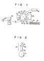
- a charger 23 is provided adjacent to a photoconductive photosensitive drum 21.
- the charger 23 evenly charges a surface of the drum 21.
- An optical writing unit 25 optically writes data in the surface of the drum 21.
- a writing controller 27 controls the unit 25 in accordance with externally supplied writing data.
- the unit 25 radiates light dots onto the surface of the drum 21, thus discharging charges on the portion irradiated with light.
- an electrostatic latent image is formed on the surface of the drum 21 by dots.
- the latent image is developed by a developer 29, and a toner image is formed on the surface of the drum 21.
- Printing paper 31 is fed from a roller 33.
- the paper 31 fed from the roller 33 is temporarily stopped by a standby roller 35.
- the paper 31 is fed to a transfer unit 37 in synchronism with the toner image formed on the surface of the drum 21.
- the paper 31 is peeled from the drum 21 by a separator 39.
- the toner image is fixed on the paper 31 by a fixer 41, and the paper is exhausted by a roller 43.
- toner particles remaining on the drum 21 are electrically neutralized by a discharger 45.
- the residual toner is cleaned by a cleaner 47.
- the charge of the surface of the drum 21 is canceled and equalized by an eraser 49.
- the optical writing unit 25 will be described in more detail with reference to Fig. 2.
- the unit 25 is constituted by a light source 51, a liquid crystal apparatus 53 and an imaging lens 55.
- light shutters of the apparatus 53 When light shutters of the apparatus 53 are turned on, light emitted from the light source 51 passes through the shutters and the lens 55 and is radiated on the surface of the drum 21.
- the lens 55 forms image of opening shutters on the drum 21 as many light dotts.
- the shutters of the apparatus 53 are turned off, light emitted from the light source 51 is shielded by the shutters and does not reach the drum 21.
- the liquid crystal apparatus 53 e.g., a G-H type liquid crystal apparatus will be described with reference to Figs. 3 to 8.
- liquid crystal apparatus 53 is formed to extend along the axial direction of the drum 21, as shown in Fig. 3.
- a plurality of light shutters S for controlling transmission of light are formed in two rows at constant intervals.
- the apparatus 53 comprises a pair of opposing transparent substrates 57 and 59 (Fig. 4).
- the transparent substrates 57 and 59 are formed of, e.g., a 0.7 mm-thick glass plate.
- the substrate 57 and 59 are adhered to each other through a frame-like outer seal member 61 and a pair of inner seal members 63 formed to be parallel to each other (Figs. 4 and 5).
- Each inner. seal member 63 is formed inside the outer seal member 61 spaced by a gap d of about 3 mm.
- the length of a small-gap portion (a liquid crystal shutter portion SP to be described later) between the inner seal members 63, i.e., the length of the inner seal members 63 is set to be 249 mm.
- the inner seal members 63, the outer seal member 61 and the substrates 57 and 59 form spaces 65 (Figs. 4 and 5). Vent holes 67 are formed in the outer seal member 61 to communicate with the spaces 65 (Fig. 5). The holes 67 are provided so as to externally evacuate air between the substrates 57 and 59. The holes 67 are sealed by seal members 69. The seal members 69 are coated after, e.g., adhering the substrates 57 and 59. Therefore, air (clean air) which is left when the substrates 57 and 59 are adhered is sealed in the spaces 65.
- the portions 71 and 73 are surrounded by the substrates 57 and 59, the inner seal members 63 and the outer seal member 61.
- the portions 71 and 73 are formed to be a rectangular box shape having a broad width.
- a liquid crystal filling hole 75 is formed in one of the portions 71 and 73 (in this embodiment in the portion 71).
- the hole 75 is formed on the central line along the width direction of the small-gap portion of the members 63.
- the hole 75 also serves as a vent hole for externally evacuating air between the substrates 57 and 59 when the substrates 57 and 59 are adhered to each other.
- a liquid crystal composition 77 is filled in the small-gap portion of the members 63 (the liquid crystal shutter portion SP) and in the portions 71 and 73 through the hole 75.
- the liquid crystal composition 77 is filled by, e.g., a vacuum filling method. After filling the liquid crystal composition 77, the hole 75 is sealed by coating a seal member 79. Note that the portions 71 and 73 are not directly associated with operation of the light shutters S, and simply store the composition 77.
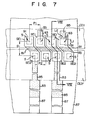
- a plurality of segment electrodes are formed on an inner surface of the substrate 57 (to be referred to as a segment substrate hereinafter) (Figs. 4, 5 and 7). These segment electrodes are formed on the small-gap portion between the members 63 in a two-row matrix form. Each segment electrode is formed to be an almost square shape having one side of about 180 ⁇ m.
- the segment electrodes constituting one row are referred to as electrodes SE1, and the segment electrodes constituting the other row are referred to as electrodes SE2 hereinafter.
- a common electrode CE1 is formed on an inner surface of the other substrate 59 (to be referred to as a common substrate hereinafter) so as to oppose the segment electrode SE1 (Figs. 4 and 6).
- a common electrode CE2 is formed on a portion of the inner surface of the substrate 59 opposing the segment electrode SE2.
- the common electrodes CE1 and CE2 have a width of, e.g., 3 mm, and are formed parallel to each other slightly spaced by about 30 pm.
- the segment electrodes SE1 and SE2 and the common electrodes CE1 and CE2 are transparent electrodes. Opposing portions of the segment electrodes SE1 and SE2 and the common electrodes CE1 and CE2 and the liquid crystal composition 77 therebetween form the light shutters S for controlling transmission of light. Portions in which the shutters S are formed and portions adjacent to the shutters S, i.e., the small-gap portion between the members 63 are together defined as the shutter portion SP.
- each segment electrode SE1 is arranged so as to be shifted by a 1/2 pitch with respect to the corresponding segment electrode SE2. Therefore, the shutters S are aligned in two rows so as to be shifted by the 1/2 pitch. This is to allow portions between points on the surface of the drum 21 irradiated with light transmitted through one row of light shutters S to be irradiated with light transmitted through the other row of shutters S, thereby forming a latent image having a high dot density on the surface of the drum 21.
- a pitch Pl or P2 distances between the centers of each two adjacent shutters
- a distance D between the centers of the shutters S in one row and those in the other row is set to be 260 ⁇ m.
- Common connecting electrodes 81 are formed on the shutter portion SP on the inner surface of the segment substrate 59. Each electrode 81 connects each segment electrode SE1 in one row and the corresponding segment electrode SE2 in the other row adjacent to the electrode SE1 shifted by the 1/2 pitch. Each electrode 81 has substantially the same width as the segment electrode.
- Driver connecting leads 83 for supplying power to the commonly connected segment electrodes are formed on the inner surface of the segment substrate 59. The leads 83 alternately extend upward and downward. The leads 83 are extended outside the outer seal member 61 and edge portions of the segment substrate 57.
- An external connecting lead 87 is formed on a distal end portion of each lead 83. The segment electrodes SE1 in one row and the segment electrodes SE2 in the other row are commonly connected for the following reason.
- each segment electrode SE1 in one row is connected to the corresponding segment electrode SE2 by one of electrodes 81.
- the common electrodes CE1 and CE2 are arranged to oppose the respective rows of segment electrodes in order to time-divisionally drive the liquid crystal apparatus.
- segment electrodes SE1 and SE2 the electrodes 81, the leads 83 and the leads 87 are integrally formed of a transparent conductive material such as indium tin oxide.
- a metal film 85 made of chromium, gold or the like is deposited on each of the electrodes 81 and the leads 83 (Figs. 4, 5, 7 and 8).
- the metal film 85 is provided so as to reduce a resistance of the electrodes 81 and the leads 83.
- the films 85 are formed on dotted portions in Fig. 7.
- each lead 83 is formed to have a width smaller than one side of the segment electrode SE1 or SE2. This is to reduce opposing areas of the leads 83 and the common electrodes CE1 and CE2. Thus, a capacitance of a capacitor constituted by the electrodes SE1, SE2, CE1 and CE2 becomes low. For this reason, even when a high frequency voltage is applied between the electrodes, a current flowing through the capacitor is low. As a result, a current flowing through the common electrodes CE1 and CE2 also becomes low, thus eliminating generation of Joule heat due to the high frequency current.
- Metal films 89 are coated on the common electrodes CE1 and CE2.
- the metal films 89 are coated excluding the shutter forming portions 91 (portions opposing the segment electrodes SE1 and SE2).
- the metal films 89 are formed on a dotted portion in Fig. 6.
- the metal films 89 are provided to reduce a resistance of the common electrodes CE1 and CE2 and to define an area of a portion through which light passing through the shutters S is transmitted.
- the shutters S are constituted by portions 91 where the common electrodes are exposed and opposed to the segment electrodes.
- Each light transmission portion (a portion from which the common electrode CE1 or CE2 is exposed) 91 is formed into a rectangle having sides of lengths Ll and L2 of 90 ⁇ m.
- the segment electrodes SE1 and SE2 and the common electrodes CE1 and CE2 are formed to a thickness of 20 nm to 30 nm, and the metal films 85 and 89 are formed to a thickness of about 170 nm.
- Liquid crystal alignment films 93 are respectively formed on the inner surfaces of the substrates 57 and 59 to a thickness 20 to 40 nm.
- an interval of the alignment films 93 at each shutter S i.e., a thickness G of the liquid crystal composition 77 at each shutter S is formed to be about 5.5 pm.
- a thickness of a liquid crystal layer between the segment electrodes SE1 and SE2 and the exposed portions 91 is formed to be about 5.5 ⁇ m.
- the inner seal members 63 are provided at two sides of the segment electrodes SE1 and SE2, thus decreasing a filling area of the composition 77.
- a width of the shutter portion SP is narrowed. This is attributed to the following reason.
- a dielectric constant of the composition 77 is larger than 1. If the filling area of the composition 77 is widened, the capacitance between the leads 83 and the common electrodes CE1 and CE2 is.increased.
- a high frequency current flows into the common electrodes CE1 and CE2 through the composition 77, thus promoting generation of the Joule heat in the common electrodes CE1 and CE2.
- the capacitance can be decreased.
- generation of heat in the common electrodes CE1 and CE2 can be reduced.
- a two-wall structure ' is adopted by using the outer seal member 61 and the inner seal members 63. For this reason, introduction of fine dust or water into the layer of the composition 77 can be completely avoided.
- Auxiliary segment electrodes SEO are formed at two sides of the segment electrodes SE1 and SE2 (Fig. 5).
- the electrodes SEO form margin erase shutters together with the common electrodes CE1 and CE2.
- the margin erase shutters are provided for irradiating two edge portions of the drum 21 (portions corresponding to margins at two sides of the recording paper) with light so as to discharge charges on the two edge portions of the drum 21.
- the margin erase shutters are driven to always be open (light can be transmitted therethrough), thereby leaving the margins at two sides of the printing paper unprinted.
- Test segment electrodes SET are formed outside of the electrodes SEO. The electrodes SET oppose the common electrodes CE1 and CE2, thus forming test shutters.
- the metal films 89 are formed so as to expose portions 95 and 97 opposing the electrodes SEO and the electrodes SET of the electrodes CE1 and CE2 (Fig. 6). Spacers 99 for keeping an interval between the substrates 57 and 59 are formed at two sides of the electrodes SET.
- a polarization plate 101 is provided on the common substrate 59.
- the liquid crystal apparatus 53 is time-divisionally driven by the two frequency addressing scheme in such a manner that a drive signal is applied between the respective segment electrodes SE1 and SE2 and the common electrodes CE1 and CE2.
- voltages having waveforms shown in Figs. 9A and 9B are applied between the electrodes, thus ON/OFF controlling the shutters S.
- a drive voltage having a waveform shown in Fig. 9A is applied between the respective segment electrodes SE1 and SE2 and the common electrodes CE1 and C E2 .
- Figs. 9A and 9B show a waveform during a period Tl for controlling the shutters S.
- the shutters S are opened/closed in response to an enable signal (a signal during a time interval T2), and are held in an open or close state in response to a hold signal (a signal during a time interval T3).
- Fig. 10A shows a voltage signal COM1 supplied to the common electrode CE1.
- Fig. 10B shows a voltage signal COM2 supplied to the common electrode CE2.
- Figs. 10C to 10F show waveforms of voltage signals SEG1 to SEG4 applied to the commonly connected segment electrodes SE1 and SE2 in synchronism with the common signals COM1 and COM2.
- the signal SEG1 is applied to open the shutters S at both the sides of the common electrodes CE1 and CE2.
- the signal SEG2 is applied to close the shutters S at the electrode CE1 side and to open the shutters S at the electrode CE2 side.
- the signal SEG3 is applied to open the shutters S at the electrode CE1 side and to close the shutters S at the electrode CE2 side.
- the signal SEG1 is applied to open the shutters S at both the sides of the electrodes CE1 and CE2.
- Figs. 10A to 10F only low frequency signal components FL and inverted signal components FL thereof are represented by pulse waveforms and high frequency signal components FH and inverted signal components FH are represented by hatched portions.
- the high frequency signal FH is applied to the common electrode CE1 during the time interval T2.
- the inverted signal f5 is applied to the electrode CE1.
- the low frequency inverted signal FL is applied to the electrode CE1
- the high frequency inverted signal FH is applied thereto
- the low frequency signal FL is applied thereto, thus ending the period Tl.
- Fig. 11A shows an electric field applied to the composition 77 between the electrodes SE1 and the common electrode CE1 when the signal SEG1 is applied to the electrodes SE1 and SE2.
- a close-activate electric field (high frequency) for horizontally aligning the liquid crystal molecules is applied to the liquid crystal composition 77 during the time interval T2, and an electric field for holding the liquid crystal molecules in a horizontally aligned state is applied during the time interval T3.
- an open-activate electric field (low frequency) for vertically aligning the liquid crystal molecules is applied, and during the next time interval T2, the close-activate electric field is applied.
- the close-activate electric field is applied immediately before the close-activate electric field is applied, if the liquid crystal molecules are vertically aligned temporarily, the liquid crystal molicules cannot be strongly aligned along a horizontal direction.
- the shutters S are opened when the open-activate electric field is applied, since an open time At is very short, it does not influence the optical recording operation.
- Fig. 11B shows an electric field applied to the liquid crystal composition 77 between the electrodes SE2 and the electrode CE2 when the signal SEG1 is applied to the electrodes SE1 and CE2.
- the electric field has the same waveform as that of the electric field shown in Fig. 11A but is shifted therefrom by half the period T1.
- Fig. 11C shows an electric field applied to the liquid crystal composition 77 between the electrodes SE1 and the electrode CE1 when the signal SEG2 is applied to the electrodes SE1 and SE2.
- Fig. 11D shows an electric field applied to the liquid crystal composition 77 between the electrodes SE2 and the electrode CE2 when the signal SEG2 is applied to the electrodes SE1 and SE2.
- the open-activate electric field is applied, and during the time interval T2, the hold electric field is applied.
- Fig. 11E shows an electric field applied to the liquid crystal composition 77 between the electrodes SE1 and the electrode CE1 when the signal SEG3 is applied to the electrodes SE1 and SE2.
- the hold electric field is applied, and during tbe time interval T3, the close-activate electric field (law frequency) is applied.
- Fig. 11F shows an electric field applied to the liquid crystal composition 77 between the electrodes SE2 and the electrode CE2 when the signal SEG3 is applied to the electrodes SE1 and SE2.
- Fig. 11F shows an electric field applied to the liquid crystal composition 77 between the electrodes SE1 and the electrode CE1 when the signal SEG4 is applied to the electrodes SE1 and SE2.
- Fig. 11H shows an electric field applied to the liquid crystal composition 77 between the electrodes SE2 and the electrode CE2 when the signal SEG4 is applied to the electrodes SE1 and SE2.
- Table 1 shows Examples 1 to 6 of the composition 77, and shows mixing ratios of various liquid crystal compounds.
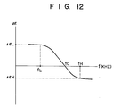
- the liquid crystal compounds of Examples 1 to 6 have the characteristics wherein the dielectric anisotropy Ae is decreased as the frequency of an applied electric field is increased, as shown in Fig. 12.
- a frequency at which the dielectric anisotropy ⁇ becomes 0 is defined as a crossing frequency fc
- a frequency 10 times the crossing frequency fc is defined as a high frequency fH
- the dielectric anisotropy at this time is defined as ⁇ H.
- a frequency 1/10 the crossing frequency fc is defined as a low frequency fL
- the dielectric anisotropy at this time is defined as AeL.
- liquid crystal compounds 1 to 21 in Table 1 are base compounds of the liquid crystal composition.
- the compounds in group I have low viscosity and good miscibility with other compounds. However, they have small dielectric anisotropy ⁇ and do not exhibit the dielectric scattering phenomenon.
- Liquid crystal compounds in group II have a large positive dielectric anisotropy AeL, exhibit the dielectric scattering phenomenon in which the absolute value of the dielectric anisotropy ⁇ H is relatively small, and have high viscosity. These compounds are used so as to give a dielectric characteristic to the liquid crystal composition.
- a liquid crystal compound in group III is used when a desired dielectric characteristic cannot be obtained only by mixing a compound in group II with one in group I.
- liquid crystal composition has a high viscosity upon mixing a compound in group II
- a compound in group III is mixed for fine-adjustment.
- a compound in group III need not be mixed when the desired dielectric characteristic can be obtained by mixing only the compound in group II.
- Liquid crystal compounds in group IV are mixed so as to decrease the dielectric characteristic of the liquid crystal composition to the negative side and to decrease the crossing frequency fc.
- the compounds in group IV have a large negative dielectric anisotropy Ae and high viscosity.
- this liquid crystal composition 77 was filled in the liquid crystal apparatus 53.
- any of the liquid crystal apparatuses in which liquid crystal compositions of respective Examples are filled requires only a very short time for switching the shutter from an open state to a close state (a time for vertically aligning the liquid crystal molecules by low frequency application after high frequency application), i.e., 0.5 ms or less. This is because in these apparatuses the absolute value of the dielectric anisotropy A E H at high frequency is large, i.e., 2.0 or more.
- liquid crystal compositions of the above Examples have a dielectric anisotropy AeL at low frequency of 3.5 or more and the ratio
- of the dielectric anisotropies is preferably set to be larger.
- a large amount of the liquid crystal compounds in group II, which is a relatively high viscosity must be mixed. Due to this, a viscosity of the liquid crystal composition becomes too high and the composition cannot be used in practice. For this reason, the ratio of the dielectric anisotropies is preferably set to be 5 or less.
- the liquid crystal apparatuses using the liquid crystal compositions of Examples 1 and 2 have excellent shutter characteristics, and those using the liquid crystal compositions of Examples 3 and 6 are second to the those of Examples 1 and 2. It is seen from these results that a liquid crystal composition in which the ratio
- all the liquid crystal apparatuses of the above Examples use the liquid crystal compositions exhibiting a dielectric scattering phenomenon in which the absolute value of the dielectric anisotropy at a high frequency is smaller than the dielectric anisotropy at a low frequency. Therefore, even after a high frequency voltage is applied for a long period of time, since the liquid crystal molecules quickly respond to low frequency application, the liquid crystal apparatus can open/close the shutters at high speed with good response time. Since the absolute value of the dielectric anisotropy AeH at high frequency and the dielectric anisotropy AeL at low frequency are set to be sufficiently large, the liquid crystal apparatus can be driven by low voltage.
- influence of the hysteresis effect of a high frequency electric field depends on the strength of the electric field.
- the electric field applied to the liquid crystal composition is strong, the hysteresis effect becomes strong.
- a strength of the electric field applied to the liquid crystal composition 77 is determined by a drive voltage and a thickness G of a layer of the liquid crystal composition 77 of the shutters shown in Fig. 8. For this reason, if the drive voltage and the thickness of the liquid crystal layer are properly selected, influence of the high frequency hysteresis effect can be reduced, and the liquid crystal molecules can respond to a low frequency voltage at high speed, thus obtaining good contrast.
- the thickness G of the liquid crystal layer becomes smaller than the above range, the electric field becomes strong and the high frequency hysteresis effect also becomes strong, thus degrading a response time. If the thickness G is set to be small, since a dye concentration in the liquid crystal composition becomes low, required light absorption cannot be performed to close the shutters S. If the thickness G is set to be large, since the strength of the electric field applied to the liquid crystal becomes low, a response time of the liquid crystal composition becomes poor.
- the liquid crystal reservoir portions 71 and 73 communicating with the liquid crystal shutter portion SP are provided.
- a change in pressure of the liquid crystal composition 77 due to a change in ambient temperature can be absorbed by a change in size of the cell container.
- a liquid crystal sealing container i.e., liquid crystal substrates and the like
- the cell container shrinks.
- test electrodes SET and seal members 99 were provided.
- the liquid crystal reservoir portions 71 and 73 are provided at two ends of the liquid crystal shutter portion SP along its lengthwise direction.
- the present invention is not limited to this.
- a single liquid crystal reservoir portion can be provided at a central portion of the liquid crystal shutter portion along its lengthwise direction.
- a position, number and structure of the liquid crystal reservoir portions are not limited to those in the above embodiment.
- a width of portions of the lead electrodes 83 opposing the common electrodes CE1 and CE2 is set to be narrower than the width of segment electrodes. For this reason, a capacitance between the lead electrodes 83 and the common electrodes CE1 and CE2 is lower than that of the conventional apparatus. Thus, when a high frequency signal is applied between the electrodes, a current flowing through the capacitance becomes low. Therefore, heat generated by this current can be reduced.
- the opposing area of the lead electrodes 83 and the common electrodes CE1 and CE2 and an increase in temperature (maximum value) due to heat generation were as shown in Table 6 when the lead electrodes SE1, SE2 had a width of 0.15 mm and the width of the lead electrodes 83 was set to be 0.3 mm, 0.15 mm and 0.1 mm.
- the width thereof is preferably set to fall within the range between 0.15 mm and 0.10 mm.
- the opposing area is preferably set to be 0.50 mm 2 or less, e.g., about 0.35 mm 2 .
- the width of the lead electrodes 83 is set to be narrower than one side of the segment electrodes SE1 and SE2 and the opposing area of the lead electrodes 83 and the common electrodes CE1 and CE2 is set to be small, heat generation can be effectively controlled, and a change and degradation in operation characteristics of the liquid crystal composition 77 can be prevented. Also, power consumption can be reduced.
- the drive voltage signal waveforms are not limited to those shown in Figs. 10A to 10F. If proper operation is assured, they can be arbitrarily set.
- a liquid crystal apparatus is used in an electrophotographic printer.
- the present invention is not limited to this, and can be applied to various types of liquid crystal apparatuses such as a television receiver, computer display and the like.
- the present invention is not limited to a liquid crystal apparatus of G-H type and can be applied to a liquid crystal apparatus of TN type.
Landscapes
- Physics & Mathematics (AREA)
- Nonlinear Science (AREA)
- Optics & Photonics (AREA)
- General Physics & Mathematics (AREA)
- Engineering & Computer Science (AREA)
- Chemical & Material Sciences (AREA)
- Crystallography & Structural Chemistry (AREA)
- General Engineering & Computer Science (AREA)
- Theoretical Computer Science (AREA)
- Mathematical Physics (AREA)
- Liquid Crystal (AREA)
Applications Claiming Priority (4)
| Application Number | Priority Date | Filing Date | Title |
|---|---|---|---|
| JP11343784U JPS6129319U (ja) | 1984-07-27 | 1984-07-27 | 液晶装置 |
| JP113437/84U | 1984-07-27 | ||
| JP59179881A JP2576085B2 (ja) | 1984-08-29 | 1984-08-29 | 液晶素子 |
| JP179881/84 | 1984-08-29 |
Publications (3)
| Publication Number | Publication Date |
|---|---|
| EP0169518A2 true EP0169518A2 (de) | 1986-01-29 |
| EP0169518A3 EP0169518A3 (en) | 1987-07-22 |
| EP0169518B1 EP0169518B1 (de) | 1991-11-21 |
Family
ID=26452414
Family Applications (1)
| Application Number | Title | Priority Date | Filing Date |
|---|---|---|---|
| EP85109091A Expired EP0169518B1 (de) | 1984-07-27 | 1985-07-22 | Flüssigkristallvorrichtung |
Country Status (3)
| Country | Link |
|---|---|
| US (2) | US4688899A (de) |
| EP (1) | EP0169518B1 (de) |
| DE (1) | DE3584697D1 (de) |
Cited By (3)
| Publication number | Priority date | Publication date | Assignee | Title |
|---|---|---|---|---|
| US4832460A (en) * | 1984-07-27 | 1989-05-23 | Casio Computer Co., Ltd. | Liquid crystal apparatus having pressure absorbing means |
| EP0251231A3 (en) * | 1986-06-30 | 1990-08-22 | Casio Computer Company Limited | Liquid crystal optical device and liquid crystal optical printer using the same |
| EP0385866A3 (de) * | 1989-02-28 | 1991-12-04 | Sony Corporation | Farbvideodrucker |
Families Citing this family (12)
| Publication number | Priority date | Publication date | Assignee | Title |
|---|---|---|---|---|
| US4759870A (en) * | 1984-08-14 | 1988-07-26 | Casio Computer Co., Ltd. | Liquid crystal composition |
| US4836654A (en) * | 1986-06-30 | 1989-06-06 | Casio Computer Co., Ltd. | Drive method for a dual-frequency, dielectric anisotropy liquid crystal optical device |
| JPH03276186A (ja) * | 1990-03-27 | 1991-12-06 | Semiconductor Energy Lab Co Ltd | 表示用基板 |
| GB9200839D0 (en) * | 1992-01-15 | 1992-03-11 | Emi Plc Thorn | Optical modulation device |
| US5936850A (en) * | 1995-03-03 | 1999-08-10 | Canon Kabushiki Kaisha | Circuit board connection structure and method, and liquid crystal device including the connection structure |
| US5953087A (en) * | 1997-04-11 | 1999-09-14 | Cambridge Research & Instrumentation Inc. | Apparatus for stress relieving liquid crystal displays |
| KR100279260B1 (ko) * | 1998-06-18 | 2001-01-15 | 김영환 | 액정 셀의 액정 주입 및 액정 주입구 봉입검사 시스템 |
| US6509947B2 (en) * | 2000-12-19 | 2003-01-21 | International Business Machines Corporation | Method and device for eliminating bubble formation within a liquid crystal display |
| WO2002092516A2 (en) * | 2001-05-11 | 2002-11-21 | Cambridge Research And Instrumentation, Inc. | Liquid crystal assembly and method of making |
| US8330693B2 (en) * | 2009-07-02 | 2012-12-11 | Teledyne Scientific & Imaging, Llc | Two-stage drive waveform for switching a dual frequency liquid crystal (DFLC) at large tilt angles |
| EP3759537B1 (de) * | 2018-03-02 | 2023-07-19 | Gooch And Housego PLC | Montagering zur bewahrung der ausrichtung einer optischen vorrichtung |
| JP7638193B2 (ja) * | 2021-10-26 | 2025-03-03 | 三菱電機株式会社 | 半導体装置および電力変換装置 |
Family Cites Families (43)
| Publication number | Priority date | Publication date | Assignee | Title |
|---|---|---|---|---|
| US3749649A (en) * | 1971-12-16 | 1973-07-31 | M & T Chemicals Inc | Bright tin-lead alloy plating |
| GB1381428A (en) * | 1972-07-04 | 1975-01-22 | Electrovac | Liquid-crystal cells |
| US3799649A (en) * | 1973-03-06 | 1974-03-26 | American Micro Syst | Haze barrier for liquid crystal display |
| US3978580A (en) * | 1973-06-28 | 1976-09-07 | Hughes Aircraft Company | Method of fabricating a liquid crystal display |
| US4009934A (en) * | 1974-01-11 | 1977-03-01 | Eastman Kodak Company | Electro-optic display devices and methods |
| GB2010560A (en) * | 1977-11-22 | 1979-06-27 | Suwa Seikosha Kk | Liquid crystal display arrangements |
| GB2013014B (en) * | 1977-12-27 | 1982-06-30 | Suwa Seikosha Kk | Liquid crystal display device |
| JPS5576393A (en) * | 1978-12-04 | 1980-06-09 | Hitachi Ltd | Matrix drive method for guestthostttype phase transfer liquid crystal |
| US4448491A (en) * | 1979-08-08 | 1984-05-15 | Canon Kabushiki Kaisha | Image display apparatus |
| NL7906695A (nl) * | 1979-09-07 | 1981-03-10 | Philips Nv | Weergeefinrichting. |
| US4386836A (en) * | 1979-12-28 | 1983-06-07 | Kabushiki Kaisha Suwa Seikosha | Electro-photographic printer |
| JPS5724917A (en) * | 1980-07-23 | 1982-02-09 | Hitachi Ltd | Multilayer liquid crystal panel |
| US4330025A (en) * | 1980-09-11 | 1982-05-18 | Allegheny Ludlum Steel Corporation | Nozzle in a strip casting apparatus |
| DE3140078A1 (de) * | 1980-10-08 | 1982-04-22 | Kabushiki Kaisha Suwa Seikosha, Tokyo | Optische fluessigkristalleinrichtung und drucker, der eine solche optische einrichtung als lichtventil benutzt |
| JPS5817414A (ja) * | 1981-07-24 | 1983-02-01 | Seiko Epson Corp | 液晶光学装置 |
| JPS58114978A (ja) * | 1981-12-28 | 1983-07-08 | Seiko Epson Corp | 液晶光学的印写装置 |
| GB2114994B (en) * | 1982-02-18 | 1984-10-10 | Suwa Seikosha Kk | Liquid crystal compositions |
| US4550981A (en) * | 1982-09-30 | 1985-11-05 | Hoffmann-La Roche Inc. | Liquid crystalline esters and mixtures |
| EP0112946B1 (de) * | 1982-12-30 | 1987-05-06 | International Business Machines Corporation | Hermetisch verschlossene elektro-optische Anzeigevorrichtung |
| NL8300817A (nl) * | 1983-03-07 | 1984-10-01 | Philips Nv | Projektiescherm. |
| JPS6065928A (ja) * | 1983-09-19 | 1985-04-15 | Toyoda Gosei Co Ltd | 液封入防振装置 |
| DE3419735C2 (de) * | 1984-05-26 | 1986-07-17 | GEA Luftkühlergesellschaft Happel GmbH & Co, 4630 Bochum | Vorrichtung zur Energieverschiebung für eine Entschwefelungsanlage |
| JPS6134134A (ja) * | 1984-07-25 | 1986-02-18 | Tanaka Kikinzoku Kogyo Kk | 装飾品用白金合金 |
| JP2576085B2 (ja) * | 1984-08-29 | 1997-01-29 | カシオ計算機株式会社 | 液晶素子 |
| US4688899A (en) * | 1984-07-27 | 1987-08-25 | Casio Computer Co., Ltd. | Dual-frequency, dielectric anisotropy liquid crystal display |
| JPS6138619A (ja) * | 1984-07-28 | 1986-02-24 | ケルンフオルシユングスツエントルム・カールスルーエ・ゲゼルシヤフト・ミツト・ベシユレンクテル・ハフツング | 煙道ガスの浄化法 |
| JPS6138616A (ja) * | 1984-07-31 | 1986-02-24 | Nippon Paionikusu Kk | ガス精製装置 |
| JPS6138618A (ja) * | 1984-07-31 | 1986-02-24 | Asahi Cokes Kogyo Kk | 廃ガスの処理方法 |
| JP2621130B2 (ja) * | 1984-08-29 | 1997-06-18 | カシオ計算機株式会社 | 液晶素子 |
| JPS6129319A (ja) * | 1985-03-11 | 1986-02-10 | 株式会社日立製作所 | 電動式吸口 |
| JPS623225A (ja) * | 1985-06-28 | 1987-01-09 | Casio Comput Co Ltd | 液晶装置 |
| JPS624727A (ja) * | 1985-07-01 | 1987-01-10 | Shiseido Co Ltd | マーブル模様の成型方法 |
| JPH0633524B2 (ja) * | 1985-07-05 | 1994-05-02 | 出光興産株式会社 | 高弾性繊維 |
| JPS6169026A (ja) * | 1985-07-17 | 1986-04-09 | Casio Comput Co Ltd | 液晶素子 |
| JPS6274219A (ja) * | 1985-09-25 | 1987-04-06 | 松下電工株式会社 | 刈込機 |
| JPS62109142A (ja) * | 1985-11-08 | 1987-05-20 | Yokogawa Electric Corp | マイクロプロセツサデバツグ装置 |
| JPS62127719A (ja) * | 1985-11-28 | 1987-06-10 | Casio Comput Co Ltd | 液晶装置 |
| JPS62127718A (ja) * | 1985-11-28 | 1987-06-10 | Casio Comput Co Ltd | 液晶装置 |
| JPS62153827A (ja) * | 1985-12-27 | 1987-07-08 | Casio Comput Co Ltd | 液晶素子 |
| JPS62153835A (ja) * | 1985-12-27 | 1987-07-08 | Casio Comput Co Ltd | 液晶素子 |
| JPS62153819A (ja) * | 1985-12-27 | 1987-07-08 | Casio Comput Co Ltd | 液晶素子 |
| JPS62153823A (ja) * | 1985-12-27 | 1987-07-08 | Casio Comput Co Ltd | 液晶シヤツタ |
| JPH06138928A (ja) * | 1992-10-26 | 1994-05-20 | Mitsubishi Electric Corp | 数値制御装置 |
-
1985
- 1985-07-11 US US06/754,397 patent/US4688899A/en not_active Expired - Fee Related
- 1985-07-22 DE DE8585109091T patent/DE3584697D1/de not_active Expired - Lifetime
- 1985-07-22 EP EP85109091A patent/EP0169518B1/de not_active Expired
-
1987
- 1987-06-26 US US07/067,449 patent/US4832460A/en not_active Expired - Fee Related
Cited By (3)
| Publication number | Priority date | Publication date | Assignee | Title |
|---|---|---|---|---|
| US4832460A (en) * | 1984-07-27 | 1989-05-23 | Casio Computer Co., Ltd. | Liquid crystal apparatus having pressure absorbing means |
| EP0251231A3 (en) * | 1986-06-30 | 1990-08-22 | Casio Computer Company Limited | Liquid crystal optical device and liquid crystal optical printer using the same |
| EP0385866A3 (de) * | 1989-02-28 | 1991-12-04 | Sony Corporation | Farbvideodrucker |
Also Published As
| Publication number | Publication date |
|---|---|
| US4832460A (en) | 1989-05-23 |
| EP0169518A3 (en) | 1987-07-22 |
| EP0169518B1 (de) | 1991-11-21 |
| DE3584697D1 (de) | 1992-01-02 |
| US4688899A (en) | 1987-08-25 |
Similar Documents
| Publication | Publication Date | Title |
|---|---|---|
| EP0169518B1 (de) | Flüssigkristallvorrichtung | |
| US4589732A (en) | Liquid crystal optical printing apparatus with rod lens | |
| US4769659A (en) | Printer utilizing optical switch elements | |
| US4548476A (en) | Time-sharing driving method for ferroelectric liquid crystal display | |
| EP0131873A1 (de) | Verfahren zum Ansteuern eines Flüssigkristallschalters für einen Drucker und entsprechender Drucker | |
| DE69119210T2 (de) | Anzeigevorrichtung | |
| US5177475A (en) | Control of liquid crystal devices | |
| US4929057A (en) | Liquid crystal optical device | |
| GB2153129A (en) | Liquid crystal display devices | |
| US7436379B2 (en) | Reversible image display medium | |
| US4745433A (en) | Image forming apparatus with a light shutter of the G-H type liquid crystal | |
| US4712878A (en) | Color image forming apparatus comprising ferroelectric smectic liquid crystal having at least two stable states | |
| US4647156A (en) | Liquid crystal device | |
| JPS6262334A (ja) | 液晶素子 | |
| JP2576085B2 (ja) | 液晶素子 | |
| JPS58176620A (ja) | 光印写装置 | |
| JP2621130B2 (ja) | 液晶素子 | |
| JP2584235B2 (ja) | 画像形成装置及びその駆動方法 | |
| JP3184761B2 (ja) | 液晶素子、それを備えた画像表示装置及び画像形成装置 | |
| DE69024907T2 (de) | Ferroelektrische Flüssigkristallvorrichtung | |
| EP0251231B1 (de) | Flüssigkristallvorrichtung und ihre Verwendung in optischen Druckern | |
| JPH0415454B2 (de) | ||
| JP3976947B2 (ja) | 電気泳動表示装置 | |
| JP4236346B2 (ja) | 書き込み装置 | |
| Tuan | Printing applications of a-Si thin film transistors |
Legal Events
| Date | Code | Title | Description |
|---|---|---|---|
| PUAI | Public reference made under article 153(3) epc to a published international application that has entered the european phase |
Free format text: ORIGINAL CODE: 0009012 |
|
| AK | Designated contracting states |
Designated state(s): CH DE FR GB LI |
|
| PUAL | Search report despatched |
Free format text: ORIGINAL CODE: 0009013 |
|
| AK | Designated contracting states |
Kind code of ref document: A3 Designated state(s): CH DE FR GB LI |
|
| 17P | Request for examination filed |
Effective date: 19871030 |
|
| 17Q | First examination report despatched |
Effective date: 19891127 |
|
| GRAA | (expected) grant |
Free format text: ORIGINAL CODE: 0009210 |
|
| AK | Designated contracting states |
Kind code of ref document: B1 Designated state(s): CH DE FR GB LI |
|
| REF | Corresponds to: |
Ref document number: 3584697 Country of ref document: DE Date of ref document: 19920102 |
|
| ET | Fr: translation filed | ||
| PLBE | No opposition filed within time limit |
Free format text: ORIGINAL CODE: 0009261 |
|
| STAA | Information on the status of an ep patent application or granted ep patent |
Free format text: STATUS: NO OPPOSITION FILED WITHIN TIME LIMIT |
|
| 26N | No opposition filed | ||
| PGFP | Annual fee paid to national office [announced via postgrant information from national office to epo] |
Ref country code: GB Payment date: 19950711 Year of fee payment: 11 Ref country code: FR Payment date: 19950711 Year of fee payment: 11 |
|
| PGFP | Annual fee paid to national office [announced via postgrant information from national office to epo] |
Ref country code: DE Payment date: 19950725 Year of fee payment: 11 |
|
| PGFP | Annual fee paid to national office [announced via postgrant information from national office to epo] |
Ref country code: CH Payment date: 19950726 Year of fee payment: 11 |
|
| PG25 | Lapsed in a contracting state [announced via postgrant information from national office to epo] |
Ref country code: GB Effective date: 19960722 |
|
| PG25 | Lapsed in a contracting state [announced via postgrant information from national office to epo] |
Ref country code: LI Effective date: 19960731 Ref country code: CH Effective date: 19960731 |
|
| GBPC | Gb: european patent ceased through non-payment of renewal fee |
Effective date: 19960722 |
|
| REG | Reference to a national code |
Ref country code: CH Ref legal event code: PL |
|
| PG25 | Lapsed in a contracting state [announced via postgrant information from national office to epo] |
Ref country code: FR Effective date: 19970328 |
|
| PG25 | Lapsed in a contracting state [announced via postgrant information from national office to epo] |
Ref country code: DE Effective date: 19970402 |
|
| REG | Reference to a national code |
Ref country code: FR Ref legal event code: ST |