EP0169820A2 - Verfahren zur Herstellung von Schutzumhüllungen, in welche entsprechende elektrisch-elektronische Bauelemente eingetaucht werden können - Google Patents
Verfahren zur Herstellung von Schutzumhüllungen, in welche entsprechende elektrisch-elektronische Bauelemente eingetaucht werden können Download PDFInfo
- Publication number
- EP0169820A2 EP0169820A2 EP85830181A EP85830181A EP0169820A2 EP 0169820 A2 EP0169820 A2 EP 0169820A2 EP 85830181 A EP85830181 A EP 85830181A EP 85830181 A EP85830181 A EP 85830181A EP 0169820 A2 EP0169820 A2 EP 0169820A2
- Authority
- EP
- European Patent Office
- Prior art keywords
- fact
- mould
- strips
- process according
- components
- Prior art date
- Legal status (The legal status is an assumption and is not a legal conclusion. Google has not performed a legal analysis and makes no representation as to the accuracy of the status listed.)
- Withdrawn
Links
Images


Classifications
-
- H—ELECTRICITY
- H10—SEMICONDUCTOR DEVICES; ELECTRIC SOLID-STATE DEVICES NOT OTHERWISE PROVIDED FOR
- H10P—GENERIC PROCESSES OR APPARATUS FOR THE MANUFACTURE OR TREATMENT OF DEVICES COVERED BY CLASS H10
- H10P72/00—Handling or holding of wafers, substrates or devices during manufacture or treatment thereof
- H10P72/04—Apparatus for manufacture or treatment
- H10P72/0444—Apparatus for wiring semiconductor or solid-state device
-
- H—ELECTRICITY
- H05—ELECTRIC TECHNIQUES NOT OTHERWISE PROVIDED FOR
- H05K—PRINTED CIRCUITS; CASINGS OR CONSTRUCTIONAL DETAILS OF ELECTRIC APPARATUS; MANUFACTURE OF ASSEMBLAGES OF ELECTRICAL COMPONENTS
- H05K7/00—Constructional details common to different types of electric apparatus
- H05K7/005—Constructional details common to different types of electric apparatus arrangements of circuit components without supporting structure
-
- H—ELECTRICITY
- H10—SEMICONDUCTOR DEVICES; ELECTRIC SOLID-STATE DEVICES NOT OTHERWISE PROVIDED FOR
- H10P—GENERIC PROCESSES OR APPARATUS FOR THE MANUFACTURE OR TREATMENT OF DEVICES COVERED BY CLASS H10
- H10P72/00—Handling or holding of wafers, substrates or devices during manufacture or treatment thereof
- H10P72/04—Apparatus for manufacture or treatment
- H10P72/0441—Apparatus for sealing, encapsulating, glassing, decapsulating or the like
-
- Y—GENERAL TAGGING OF NEW TECHNOLOGICAL DEVELOPMENTS; GENERAL TAGGING OF CROSS-SECTIONAL TECHNOLOGIES SPANNING OVER SEVERAL SECTIONS OF THE IPC; TECHNICAL SUBJECTS COVERED BY FORMER USPC CROSS-REFERENCE ART COLLECTIONS [XRACs] AND DIGESTS
- Y10—TECHNICAL SUBJECTS COVERED BY FORMER USPC
- Y10S—TECHNICAL SUBJECTS COVERED BY FORMER USPC CROSS-REFERENCE ART COLLECTIONS [XRACs] AND DIGESTS
- Y10S29/00—Metal working
- Y10S29/048—Welding with other step
-
- Y—GENERAL TAGGING OF NEW TECHNOLOGICAL DEVELOPMENTS; GENERAL TAGGING OF CROSS-SECTIONAL TECHNOLOGIES SPANNING OVER SEVERAL SECTIONS OF THE IPC; TECHNICAL SUBJECTS COVERED BY FORMER USPC CROSS-REFERENCE ART COLLECTIONS [XRACs] AND DIGESTS
- Y10—TECHNICAL SUBJECTS COVERED BY FORMER USPC
- Y10T—TECHNICAL SUBJECTS COVERED BY FORMER US CLASSIFICATION
- Y10T29/00—Metal working
- Y10T29/49—Method of mechanical manufacture
- Y10T29/49002—Electrical device making
- Y10T29/49117—Conductor or circuit manufacturing
- Y10T29/49169—Assembling electrical component directly to terminal or elongated conductor
- Y10T29/49171—Assembling electrical component directly to terminal or elongated conductor with encapsulating
- Y10T29/49172—Assembling electrical component directly to terminal or elongated conductor with encapsulating by molding of insulating material
-
- Y—GENERAL TAGGING OF NEW TECHNOLOGICAL DEVELOPMENTS; GENERAL TAGGING OF CROSS-SECTIONAL TECHNOLOGIES SPANNING OVER SEVERAL SECTIONS OF THE IPC; TECHNICAL SUBJECTS COVERED BY FORMER USPC CROSS-REFERENCE ART COLLECTIONS [XRACs] AND DIGESTS
- Y10—TECHNICAL SUBJECTS COVERED BY FORMER USPC
- Y10T—TECHNICAL SUBJECTS COVERED BY FORMER US CLASSIFICATION
- Y10T29/00—Metal working
- Y10T29/49—Method of mechanical manufacture
- Y10T29/49002—Electrical device making
- Y10T29/49117—Conductor or circuit manufacturing
- Y10T29/49174—Assembling terminal to elongated conductor
- Y10T29/49176—Assembling terminal to elongated conductor with molding of electrically insulating material
-
- Y—GENERAL TAGGING OF NEW TECHNOLOGICAL DEVELOPMENTS; GENERAL TAGGING OF CROSS-SECTIONAL TECHNOLOGIES SPANNING OVER SEVERAL SECTIONS OF THE IPC; TECHNICAL SUBJECTS COVERED BY FORMER USPC CROSS-REFERENCE ART COLLECTIONS [XRACs] AND DIGESTS
- Y10—TECHNICAL SUBJECTS COVERED BY FORMER USPC
- Y10T—TECHNICAL SUBJECTS COVERED BY FORMER US CLASSIFICATION
- Y10T29/00—Metal working
- Y10T29/49—Method of mechanical manufacture
- Y10T29/49789—Obtaining plural product pieces from unitary workpiece
-
- Y—GENERAL TAGGING OF NEW TECHNOLOGICAL DEVELOPMENTS; GENERAL TAGGING OF CROSS-SECTIONAL TECHNOLOGIES SPANNING OVER SEVERAL SECTIONS OF THE IPC; TECHNICAL SUBJECTS COVERED BY FORMER USPC CROSS-REFERENCE ART COLLECTIONS [XRACs] AND DIGESTS
- Y10—TECHNICAL SUBJECTS COVERED BY FORMER USPC
- Y10T—TECHNICAL SUBJECTS COVERED BY FORMER US CLASSIFICATION
- Y10T29/00—Metal working
- Y10T29/49—Method of mechanical manufacture
- Y10T29/4998—Combined manufacture including applying or shaping of fluent material
Definitions
- the invention relates to a process for producing protective envelopes in which corresponding electric-electronic circuit components are dipped.
- a process called "surface mounting” is known with which circuit components are subjected to the direct action of heat at the time the electrical terminations thereof are being welded to printed circuit conductor tracks.
- the component itself withstands the welding temperature (on an average around 260 0 0), as in the case of ceramic components, or the component has to be given a suitable protective envelope (capsule) of insulating material (for example synthetic resin), otherwise the said component would be destroyed.
- the component be positioned up against one side of the printed circuit board so that the individual electrical terminations mate with corresponding conductor tracks, that the said positioning be rendered stable (for example by bonding the component to the said side), and then that the terminations be welded to the tracks.
- the heat hits directly the side of the board on which the components are placed; if the components were not protected in an envelope able to resist the welding temperature, the heat would ruin them.
- the proc&ss according to the invention belongs to the particular technical field concerned with the production of protective envelopes for circuit components destined, out of preference, to be mounted in the way to which reference has just been made.
- the process proposed herein concerns the production of protective envelopes for electric-electronic components destined, for example, to be "surface mounted" on corresponding printed circuits in a sequence of elementary phases that do not necessitate the use either of injection moulds or of complicated items of equipment, and with which the use is possible of the material most suited to the particular ap- plioation to which the protectively enveloped components in question are to be put and, furthermore, that render the process extremely flexible as regards variations in the dimensions of the protective envelopes in accordance with the requirements.
- the foregoing being achievable with a notable reduction in costs compared to the envelopes produced up until now.
- the process according to the invention for producing protective envelopes in which corresponding electric-electronic circuit components are dipped is characterized by the following phases: a) the formation of a plurality of flat or filiform conductor elements; b) the connection, by means of welding, of the free ends of each of the said circuit components to corresponding conductor elements; c) the creation of a mould in which there is at least one longitudinal impression, suitable to receive a circuit components unit pre-equipped with corresponding conductor elements, placed orderly side-by-side and spaced one from the other; d) the stable insertion into the mould of the said unit with the circuit components positioned in the said impression; e) the pouring of a liquid sealant into the said impression so as to cover only the unit components, then left to set; f) the separation, one from the other, of the said mould and the one piece block thus formed of hardened sealant in which the said circuit components are dipped, from which the said conductor elements at least partially project; g) the formation, from the said one piece block
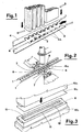
- the first phase in the process envisages the creation of two conductor strips (1), each of which provided, along one longitudinal edge, with end pieces (2) whose external parts (2a) (having therein corresponding through holes) are bent on one and the same side and, in particular, at a right angle with respect to the plane defined by the corresponding strip.
- the strips are identical, while the end pieces are equidistant one with respect to the other.
- the element (4) out of which, first of all, the end pieces are fashioned and then the part (2a) thereof is bent downwards.
- each end piece of a strip be opposite a corresponding end piece of the other strip.
- the electrical connection through welding, is envisaged of the free ends (6a) of electric-electronic components (6) (in the example given in Fig. 2, capacative components) to the bent parts (2a) of two opposite corresponding end pieces (2), thereby making possible the construction of a unit constituted by the two strips (1) and by the plurality of components (8) looked to the said strips.
- Fig. 2 in which at (7) are shown known means for effecting the union of the free ends (6a) to the parts (2a) by means of electrical spot welding.
- a mould (9) produced through the permanent cold deformation of a sheet (9a), interposing the said sheet between a punch (10a) and a die (10b). The insertion of the punch into the die causes a mould to be created.
- the material used for the sheet (9a) (for example a sheet of aluminium lined with a layer of polyethylene) must have the features described below.
- the conformation of the mould is such as to be provided with two longitudinal seats (11) able to receive resting thereon, the strips (1) of a corresponding unit (8), in between which provision is made for a longitudinal impression ( 1 2) wherein the components (6) of the said unit are freely accepted (.see Fig. 4).
- the forming of the mould constitutes a further phase in the process in question, and more precisely the third phase thereof, though this phase does not necessarily have to follow on, in the order stated, after the two previously mentioned phases.
- the strips (1) After the unit has been inserted into the mould (9), the strips (1) have to be secured to the seats (11); this can be achieved in various ways, for example through the heat sealing method using the known means (13a) and (13b) shown diagrammatically in Fig. 5. It must be stressed that the polyethylene layer notably contributes to the said operation.
- the pouring is envisaged of the liquid sealant (14) (for example thermosetting or thermoplastic resin etcetera) into the impression (12) in the mould (9) until the components (6) have been covered completely but without the sealant reachiug the strips (1); indeed in the case under examination (see Fig. 6), it is sufficient for the level of the sealant to be slightly below the plane defined by the seats (11) in the mould (9). The situation to which reference has just been made is maintained until the sealant (14) has fully set. Once this is - so, the one piece block (16) formed by the sealant in which the components (6) are dipped and from which the end pieces (2) partially project and from which the strips (1) fully project, is separated from the mould (9) (see Fig. 7), this operation defining the sixth phase of the process.
- the liquid sealant (14) for example thermosetting or thermoplastic resin etcetera
- the sealant (14) is constituted by liquid resir., it is necessary that the material used in the making of the mould (9) be able to withstand, without becoming misshapen, the temperature of the said liquid resin (14) and, furthermore, that it allows the quick and simple separation of the one piece block (16) from the mould (9) which is of the type used once only and then discarded.
- the definition should take place of the electrical terminations (17) of the components (6) embedded in the one piece block (16), with the formation there from of small blocks (21), each of which constituted by solidified sealant in which the corresponding circuit component (6) is embedded, and from which project the electrical terminations (17) of the said individual components.
- Two possibilities are envisaged, as shown in the accompanying figures, for the definition of the said electrical terminations.
- the areas (1a) of a strip (1) in between the end pieces (2) are cut (using known means (18).
- the longitudinal cutting is effected of the end pieces at points corresponding to the areas where they are joined to corresponding strips.
- the said electrical terminations (17) are defined by the internal parts of the end pieces (2).
- the one piece block (16) got ready in this way enables the components embedded therein to be tested in a fast and efficient manner.
- the unit (8) i-s defined, in the variant to which reference has just been made, by a plurality of components (6) provided with the said conductor elements, placed side-by-side in an orderly fashion, one spaced away from the other.
- the internal extremities of the said elements are rested on the seats (11) of the mould, and to these are bonded in a known fashion, for example through the previously mentioned heat-sealing method.
- a further possible variant would be to provide a frame whose longitudinal sides are constituted by the strips (1), with the said strips connected by at least two transverse strengthening elements.
- the electrical terminations (17) can be bent in any way with respect to the one piece block (16), for example closely up against the longitudinal sides of the block (as in Fig. 9), or upwards etcetera.
- the said terminations can also be utilized as oriented at the time of the definition thereof: in this case there is no need for them to be bent.
- one mould (9) can be utilized for units that are not all alike, that is to say, for units whose components differ (from unit to unit) in the longitudinal dimensions thereof, provided that the said dimensions can be freely accepted in the impression (12).
- sealant (14) used in this process has to be selected to suit the type of electric-electronic component to be protected, to suit the use to which the said component is to be put and, lastly, to suit the environment in which the said component is going to operate, though principally the protective envelope has to safeguard efficiently the component at the time of the welding of the electrical terminations (17) to the conductor tracks of the printed circuit, thereby fulfilling the technical task of the invention.
- the mould (9) into which the sealant is poured takes the form shown in Fig. 3, though it is obvious that any other type of mould can be employed (also constituted by two or more elements assembled together and interlocked) such as to have seats on which the strips or internal extremities of the said flat and/or filiform conductor elements can rest, an impression that accepts the components of the unit (3) and, lastly, such as to allow the dipping with sealant solely of the components without the internal parts of the end pieces being affected.
- the shape of the end pieces (2) (in particular the external parts (2a)), or as regards the stated variant, the shape of the conductor elements (in particular the external extremities), must be such as to facilitate the welding thereof to the free ends (6a) of the components (6). This is of the utmost importance for the purpose of achieving between the end pieces (or the conductor elements) and the component, optimum mechanical anchoring and electrical connection.
- Blocks (21) without clinched terminations, having instead terminations (17) in the form of terminals, serve efficiently for mounting on conventional printed circuits (that is to say the ones provided with a through hole for each component), this form of installation being accomplished by inserting the terminals through the through holes and then effecting a soldering operation.
Landscapes
- Engineering & Computer Science (AREA)
- Microelectronics & Electronic Packaging (AREA)
- Casings For Electric Apparatus (AREA)
- Structures Or Materials For Encapsulating Or Coating Semiconductor Devices Or Solid State Devices (AREA)
- Apparatuses And Processes For Manufacturing Resistors (AREA)
- Manufacturing Of Electrical Connectors (AREA)
- Insulating Of Coils (AREA)
- Casting Or Compression Moulding Of Plastics Or The Like (AREA)
- Encapsulation Of And Coatings For Semiconductor Or Solid State Devices (AREA)
Applications Claiming Priority (2)
| Application Number | Priority Date | Filing Date | Title |
|---|---|---|---|
| IT03538/84A IT1180514B (it) | 1984-07-27 | 1984-07-27 | Procedimento per la realizzazione di involucri protettivi in cui risultano annegati corrispondenti componenti elettrico elettronici |
| IT353884 | 1984-07-27 |
Publications (2)
| Publication Number | Publication Date |
|---|---|
| EP0169820A2 true EP0169820A2 (de) | 1986-01-29 |
| EP0169820A3 EP0169820A3 (de) | 1987-08-26 |
Family
ID=11109286
Family Applications (1)
| Application Number | Title | Priority Date | Filing Date |
|---|---|---|---|
| EP85830181A Withdrawn EP0169820A3 (de) | 1984-07-27 | 1985-07-12 | Verfahren zur Herstellung von Schutzumhüllungen, in welche entsprechende elektrisch-elektronische Bauelemente eingetaucht werden können |
Country Status (9)
| Country | Link |
|---|---|
| US (1) | US4720916A (de) |
| EP (1) | EP0169820A3 (de) |
| JP (1) | JPS6147602A (de) |
| KR (1) | KR900001116B1 (de) |
| ES (1) | ES8609872A1 (de) |
| FI (1) | FI852577L (de) |
| GR (1) | GR851658B (de) |
| IT (1) | IT1180514B (de) |
| PT (1) | PT80874B (de) |
Families Citing this family (1)
| Publication number | Priority date | Publication date | Assignee | Title |
|---|---|---|---|---|
| JPS631109A (ja) * | 1986-06-19 | 1988-01-06 | Murata Mfg Co Ltd | 電子部品およびその製造方法 |
Family Cites Families (13)
| Publication number | Priority date | Publication date | Assignee | Title |
|---|---|---|---|---|
| US3076051A (en) * | 1959-03-05 | 1963-01-29 | Rca Corp | Thermoelectric devices and methods of making same |
| US3340347A (en) * | 1964-10-12 | 1967-09-05 | Corning Glass Works | Enclosed electronic device |
| US3364567A (en) * | 1965-09-14 | 1968-01-23 | Bell Telephone Labor Inc | Encapsulated electrical device and method of fabricating same |
| US3530541A (en) * | 1968-06-13 | 1970-09-29 | Trw Inc | Mold for encapsulating electrical components |
| FR2076686A5 (de) * | 1970-01-23 | 1971-10-15 | Sovcor Electronique | |
| US3838316A (en) * | 1973-10-09 | 1974-09-24 | Western Electric Co | Encapsulated electrical component assembly and method of fabrication |
| SE389991B (sv) * | 1974-09-19 | 1976-11-29 | Ericsson Telefon Ab L M | Metod for kapsling av elektriska komponenter samt anordning herfor |
| US4079511A (en) * | 1976-07-30 | 1978-03-21 | Amp Incorporated | Method for packaging hermetically sealed integrated circuit chips on lead frames |
| US4268942A (en) * | 1979-09-04 | 1981-05-26 | Western Electric Company, Inc. | Method and apparatus for manufacturing boxed encapsulated capacitors |
| DE2952297A1 (de) * | 1979-12-24 | 1981-07-02 | Werner Dipl.-Ing. 6840 Lampertheim Schaller | Verfahren und vorrichtung zur herstellung von elektronischen geraeten, insbesondere beruehrungslosen sensoren und modulen |
| US4330790A (en) * | 1980-03-24 | 1982-05-18 | National Semiconductor Corporation | Tape operated semiconductor device packaging |
| US4374080A (en) * | 1981-01-13 | 1983-02-15 | Indy Electronics, Inc. | Method and apparatus for encapsulation casting |
| US4451973A (en) * | 1981-04-28 | 1984-06-05 | Matsushita Electronics Corporation | Method for manufacturing a plastic encapsulated semiconductor device and a lead frame therefor |
-
1984
- 1984-07-27 IT IT03538/84A patent/IT1180514B/it active
-
1985
- 1985-06-28 FI FI852577A patent/FI852577L/fi not_active Application Discontinuation
- 1985-07-04 GR GR851658A patent/GR851658B/el unknown
- 1985-07-12 EP EP85830181A patent/EP0169820A3/de not_active Withdrawn
- 1985-07-19 KR KR1019850005146A patent/KR900001116B1/ko not_active Expired
- 1985-07-26 PT PT80874A patent/PT80874B/pt unknown
- 1985-07-26 JP JP60165619A patent/JPS6147602A/ja active Pending
- 1985-07-26 ES ES545564A patent/ES8609872A1/es not_active Expired
-
1986
- 1986-10-08 US US06/915,877 patent/US4720916A/en not_active Expired - Fee Related
Also Published As
| Publication number | Publication date |
|---|---|
| EP0169820A3 (de) | 1987-08-26 |
| GR851658B (de) | 1985-11-26 |
| ES8609872A1 (es) | 1986-09-01 |
| FI852577A7 (fi) | 1986-01-28 |
| PT80874B (en) | 1986-11-24 |
| IT1180514B (it) | 1987-09-23 |
| ES545564A0 (es) | 1986-09-01 |
| US4720916A (en) | 1988-01-26 |
| FI852577A0 (fi) | 1985-06-28 |
| KR860001499A (ko) | 1986-02-26 |
| IT8403538A0 (it) | 1984-07-27 |
| PT80874A (en) | 1985-08-01 |
| FI852577L (fi) | 1986-01-28 |
| KR900001116B1 (ko) | 1990-02-26 |
| JPS6147602A (ja) | 1986-03-08 |
Similar Documents
| Publication | Publication Date | Title |
|---|---|---|
| DE4421077B4 (de) | Halbleitergehäuse und Verfahren zu dessen Herstellung | |
| DE69212185T2 (de) | Halbleiteraufbau mit flexibler Trägerfolie | |
| DE1489781B2 (de) | Hermetisches gehaeuse fuer eine elektronische vorrichtung, vorzugsweise miniaturvorrichtung, und verfahren zu seiner herstellung | |
| JPH07169903A (ja) | 集積回路パッケージ | |
| DE102008061636A1 (de) | Halbleitervorrichtung und Verfahren zu deren Herstellung | |
| DE3623419C2 (de) | ||
| DE19743537A1 (de) | Halbleitergehäuse für Oberflächenmontage sowie Verfahren zu seiner Herstellung | |
| US6694610B1 (en) | Method of producing electronic component | |
| EP0969502B1 (de) | Harzverkapselte elektronische Bauteile und deren Herstellungsverfahren | |
| EP0548496B1 (de) | Form und Verfahren zur Herstellung von Kunststoffpackungen für integrierte Schaltungen die eine freie metallische Wärmesenke enthalten zur Inspektion der Lötverbindung | |
| EP0169820A2 (de) | Verfahren zur Herstellung von Schutzumhüllungen, in welche entsprechende elektrisch-elektronische Bauelemente eingetaucht werden können | |
| DE4436523A1 (de) | Verfahren zur Herstellung eines elektronischen Gerätes und Drehzahlsensor mit einer elektronischen Schaltung | |
| DE19927947A1 (de) | Verfahren zum Herstellen eines Drahteinlageinduktors und durch dasselbe hergestellter Drahteinlageinduktor | |
| US4724280A (en) | Package for integrated circuit | |
| US3417193A (en) | Electrical module having terminals made from semicircular wire and method of making the same | |
| DE102004033284A1 (de) | Verfahren und Vorrichtung zur Herstellung einer elektrischen und mechanischen Verbindung sowie eines Kunststoffvergusses von Teilen | |
| US3426426A (en) | Sliced circuitry | |
| JP3293105B2 (ja) | 半導体中間構体及びその樹脂モールド装置 | |
| JPH087645Y2 (ja) | 面実装用icパッケージ | |
| JPH04164383A (ja) | 金属プリント基板およびその製造方法 | |
| JPH0334848Y2 (de) | ||
| DE102024126452A1 (de) | Leistungsmodul-Grundplatte und Leistungsmodul | |
| JPS59108335A (ja) | 半導体装置の製造方法 | |
| JPH05206355A (ja) | ハイブリット集積回路装置におけるリード端子の装着方法 | |
| JPS60240181A (ja) | 電子部品 |
Legal Events
| Date | Code | Title | Description |
|---|---|---|---|
| PUAI | Public reference made under article 153(3) epc to a published international application that has entered the european phase |
Free format text: ORIGINAL CODE: 0009012 |
|
| AK | Designated contracting states |
Designated state(s): AT BE CH DE FR GB LI LU NL SE |
|
| RTI1 | Title (correction) | ||
| PUAL | Search report despatched |
Free format text: ORIGINAL CODE: 0009013 |
|
| AK | Designated contracting states |
Kind code of ref document: A3 Designated state(s): AT BE CH DE FR GB LI LU NL SE |
|
| 17P | Request for examination filed |
Effective date: 19870916 |
|
| 17Q | First examination report despatched |
Effective date: 19891212 |
|
| STAA | Information on the status of an ep patent application or granted ep patent |
Free format text: STATUS: THE APPLICATION IS DEEMED TO BE WITHDRAWN |
|
| 18D | Application deemed to be withdrawn |
Effective date: 19920121 |
|
| RIN1 | Information on inventor provided before grant (corrected) |
Inventor name: VENTURA, GIORGIO |