EP0169980A2 - In vordiffundiertem, integrierten Schaltkeis hergestellter Festwertspeicher - Google Patents
In vordiffundiertem, integrierten Schaltkeis hergestellter Festwertspeicher Download PDFInfo
- Publication number
- EP0169980A2 EP0169980A2 EP85104890A EP85104890A EP0169980A2 EP 0169980 A2 EP0169980 A2 EP 0169980A2 EP 85104890 A EP85104890 A EP 85104890A EP 85104890 A EP85104890 A EP 85104890A EP 0169980 A2 EP0169980 A2 EP 0169980A2
- Authority
- EP
- European Patent Office
- Prior art keywords
- type
- memory
- transistors
- integrated circuit
- read
- Prior art date
- Legal status (The legal status is an assumption and is not a legal conclusion. Google has not performed a legal analysis and makes no representation as to the accuracy of the status listed.)
- Withdrawn
Links
Images

Classifications
-
- G—PHYSICS
- G11—INFORMATION STORAGE
- G11C—STATIC STORES
- G11C17/00—Read-only memories programmable only once; Semi-permanent stores, e.g. manually-replaceable information cards
- G11C17/08—Read-only memories programmable only once; Semi-permanent stores, e.g. manually-replaceable information cards using semiconductor devices, e.g. bipolar elements
- G11C17/10—Read-only memories programmable only once; Semi-permanent stores, e.g. manually-replaceable information cards using semiconductor devices, e.g. bipolar elements in which contents are determined during manufacturing by a predetermined arrangement of coupling elements, e.g. mask-programmable ROM
- G11C17/12—Read-only memories programmable only once; Semi-permanent stores, e.g. manually-replaceable information cards using semiconductor devices, e.g. bipolar elements in which contents are determined during manufacturing by a predetermined arrangement of coupling elements, e.g. mask-programmable ROM using field-effect devices
Definitions
- the present invention relates to a read only memory produced in a prediffused integrated circuit.
- prediffused integrated circuit is understood to mean a set of transistors, for example of the MOS type, which are made in advance on the same semiconductor substrate, according to a regular structure independent of the function to be performed subsequently by this integrated circuit, and which are then interconnected on demand, depending on the type of function to be performed by this integrated circuit, a certain number of areas reserved for interconnections being provided for this on the surface of the integrated circuit.
- This technique has the advantage of concentrating on the final phase of the manufacturing process the production of the "personalized” part of the integrated circuit, namely the interconnections, and of carrying over to the previous phases the production of the "standard” part of a integrated circuit, common to all users.
- the interconnections represent a network essentially arranged between these rows (there are in fact a certain number of interconnections in the rows themselves).
- the difficulty can be such that the manufacturers of integrated circuits are brought to modify the "standard" part of the circuit to grant a larger place to the zones reserved for interconnections, which results of course in a loss of performance for all the users, that is to say whatever the function to be performed.
- the transistors are arranged in rows, or lines, which are alternately of type N and of type P, and are grouped in basic cells each comprising two transistors of type N and two transistors of type P, belonging to two rows and two adjacent columns. These basic cells are such that two adjacent transistors of the same line have a common transfer electrode (drain or source), and that two adjacent transistors of the same column have their control electrode combined.
- the present invention relates to the production of a read-only memory (or ROM) in an integrated circuit, more particularly of the pre-broadcast type with free interconnections. It relates more specifically to a read-only memory in which each memory point (or elementary memory cell) is produced by means of a MOS switch, itself produced by means of two MOS transistors, one of type P, the other of type N, in parallel, i.e. having one of their transfer electrodes joined to form the input of the switch (to which the logic level to be memorized is applied) and the other transfer electrode joined to form the switch output, their repective control electrode (or grid) receiving two complementary control signals (A, A) representing the control of the switch.
- N x P switches due to the control of the two transistors constituting a switch by means of two complementary signals, with the conventional prediffused integrated circuits, with gates joined, the production of N x P switches implies the use of N x P cells of basis of this circuit, of which two out of four transistors are unused.
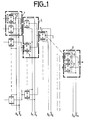
- FIG. 1 Another structure has been proposed (shown in FIG. 1), consisting in assigning these two unused transistors to the production of another memory point, ie in total two memory points per base cell, that is to say, for each of the P binary elements, a set of N basic cells such as the basic cell 1.
- the command of one of the memory points of each base cell is necessarily dependent (more precisely, complementary) on the command of the other memory point, hence the need for a "pyramid" structure, in which the N switches, such as switch 2, thus obtained have their outputs connected two by two, are controlled by the same signals A 0 , A 0 , - and are followed by a similar set of switches, such as switch 3, (i.e.
- the subject of the present invention is a different structure, suitable for integrated circuits of the prediffused type with free interconnections, and making it possible to reduce in significantly greater numbers the number of basic cells of an integrated circuit necessary for the production of a memory. dead.
- the read-only memory according to the invention with N words of P binary elements, of the type with MOS switches capable of providing on their output a logic state permanently applied to their input, produced in an integrated circuit of the prediffused type comprising rows of transistors Alternately P-type and N-type MOS, with gates not joined from one row to another, organized in basic cells each comprising two adjacent P-type transistors and two adjacent N-type transistors of two adjacent rows, comprises basic cells arranged in the form of a matrix rows and P columns, the transistors of each of these basic cells being mounted so as to produce two switches on the inputs of which are applied logical states corresponding to two binary elements of the same rank p of two words of different ranks n (n and p varying respectively from 0 to N-1 and from 0 to P-1), the outputs of these two switches being combined, all the outputs thus obtained for all the basic cells arranged in the same column of row p being combined to form the output of row p of the memory, and all the basic cells arranged in the same row of rank
- the read only memory represented in FIG. 2 is a read memory with N words of P binary elements. It is carried out with only N P base cells, such as base cell 10, of a pre-broadcast integrated circuit with free interconnections, each comprising two independently controlled memory points. Each memory point is produced by means of a MOS switch itself comprising two MOS transistors in parallel of opposite types (N and P) and with non-joined gates, such as switches 11 and 12.
- the basic cells of this memory are arranged in the form of a matrix with 2 rows and P columns, which, taking into account the matrix organization of the basic cells of an integrated circuit non-interconnected, and unlike the previous pyramid structure, simplifies interconnections and ensures optimal compactness.
- the two memory points of each basic cell have their outputs combined and memorize a binary element of the same rank of two successive words.
- the two memory points of. the basic cell 10 located at the intersection of the second row and first column respectively store the bit of rank 0 of the 2 nd word (I 02) and the bit of rank 0 of the 3rd word (I 03).
- All the outputs of the basic cells located on the same column are combined to provide, when this memory is read, a binary element of given rank of the word selected by addressing the memory.
- the basic cells of the first column provide the binary element of rank 0, I 0 , of the selected word.
- the memory is addressed by controlling the gates of all the transistors forming this memory. L being exclusive by words, and each basic cell comprising two memory points, all the cells of the same line are controlled by the same signals, which are four in number, such as the signals A 0 , A 1 for the first line, the signals A 0 and 0 intervening for the control of one of the two memory points of each base cell, and the signals A and A 1 for the control of the other memory point.
- this memory has another advantage which is its ease of extension, due to the repeatability of its structure.
Landscapes
- Semiconductor Memories (AREA)
- Design And Manufacture Of Integrated Circuits (AREA)
- Read Only Memory (AREA)
Applications Claiming Priority (2)
| Application Number | Priority Date | Filing Date | Title |
|---|---|---|---|
| FR8406702A FR2563651B1 (fr) | 1984-04-27 | 1984-04-27 | Memoire morte realisee en circuit integre prediffuse |
| FR8406702 | 1984-04-27 |
Publications (2)
| Publication Number | Publication Date |
|---|---|
| EP0169980A2 true EP0169980A2 (de) | 1986-02-05 |
| EP0169980A3 EP0169980A3 (de) | 1986-02-12 |
Family
ID=9303578
Family Applications (1)
| Application Number | Title | Priority Date | Filing Date |
|---|---|---|---|
| EP85104890A Withdrawn EP0169980A3 (de) | 1984-04-27 | 1985-04-23 | In vordiffundiertem, integrierten Schaltkeis hergestellter Festwertspeicher |
Country Status (3)
| Country | Link |
|---|---|
| EP (1) | EP0169980A3 (de) |
| JP (1) | JPS60239998A (de) |
| FR (1) | FR2563651B1 (de) |
Cited By (2)
| Publication number | Priority date | Publication date | Assignee | Title |
|---|---|---|---|---|
| EP0206229A3 (en) * | 1985-06-18 | 1988-04-06 | Kabushiki Kaisha Toshiba | Semiconductor memory device |
| EP0434104A1 (de) * | 1989-11-15 | 1991-06-26 | Koninklijke Philips Electronics N.V. | Integrierte Halbleiterschaltung vom Master-slice-Typ |
Families Citing this family (2)
| Publication number | Priority date | Publication date | Assignee | Title |
|---|---|---|---|---|
| JPS61289598A (ja) * | 1985-06-17 | 1986-12-19 | Toshiba Corp | 読出専用半導体記憶装置 |
| US6969810B1 (en) * | 2004-05-25 | 2005-11-29 | Rockwell Automation Technologies, Inc. | Electric key switch with key sensing and ejection |
Family Cites Families (3)
| Publication number | Priority date | Publication date | Assignee | Title |
|---|---|---|---|---|
| JPS6028078B2 (ja) * | 1980-06-19 | 1985-07-02 | 三菱電機株式会社 | メモリ読出し回路 |
| JPS5728364A (en) * | 1980-07-28 | 1982-02-16 | Fujitsu Ltd | Semiconductor memory device |
| FR2524206B1 (fr) * | 1982-03-26 | 1985-12-13 | Thomson Csf Mat Tel | Circuit integre prediffuse, et procede d'interconnexion des cellules de ce circuit |
-
1984
- 1984-04-27 FR FR8406702A patent/FR2563651B1/fr not_active Expired
-
1985
- 1985-04-23 EP EP85104890A patent/EP0169980A3/de not_active Withdrawn
- 1985-04-25 JP JP60089876A patent/JPS60239998A/ja active Pending
Cited By (3)
| Publication number | Priority date | Publication date | Assignee | Title |
|---|---|---|---|---|
| EP0206229A3 (en) * | 1985-06-18 | 1988-04-06 | Kabushiki Kaisha Toshiba | Semiconductor memory device |
| US4873670A (en) * | 1985-06-18 | 1989-10-10 | Kabushiki Kaisha Toshiba | Complementary semiconductor memory device with pull-up and pull down |
| EP0434104A1 (de) * | 1989-11-15 | 1991-06-26 | Koninklijke Philips Electronics N.V. | Integrierte Halbleiterschaltung vom Master-slice-Typ |
Also Published As
| Publication number | Publication date |
|---|---|
| FR2563651A1 (fr) | 1985-10-31 |
| JPS60239998A (ja) | 1985-11-28 |
| EP0169980A3 (de) | 1986-02-12 |
| FR2563651B1 (fr) | 1986-06-27 |
Similar Documents
| Publication | Publication Date | Title |
|---|---|---|
| FR2600453A1 (fr) | Dispositif de memoire a semi-conducteurs | |
| EP0298002A1 (de) | Transpositionsspeicher für eine Datenverarbeitungsschaltung | |
| FR2515875A1 (fr) | Circuit de chaine de transistors a effet de champ | |
| FR2563651A1 (fr) | Memoire morte realisee en circuit integre prediffuse | |
| EP0011700B1 (de) | Stromversorgungs-Vorrichtung für monolithische Speicher | |
| FR2600793A1 (fr) | Procede d'etude de microcalculateurs integres et microcalculateurs integres a structure modulaire obtenus par ce procede | |
| EP0170777A1 (de) | Elementare dynamische Speicherzellen und dynamischer Speicher, ausgeführt durch Vereinigung solcher elementaren Zellen | |
| EP2366246B1 (de) | Integriertes schaltungsarray und insbesondere gross bemessener bildsensor | |
| EP0183610A1 (de) | Schreib-Lese-Speicher und Anwendung in einer linearen Interpolationsschaltung | |
| EP1187142B1 (de) | Zwischenspeicherzelle mit Maskierung und gleicher Anzahl von N-Kanal Transistoren und P-Kanal Transistoren | |
| EP0140413B1 (de) | Dekodierschaltung für statischen RAM-Speicher | |
| EP0237425B1 (de) | Integrierter Schaltkreis von neuartiger Architektur und sein Hertellungsverfahren | |
| FR2837621A1 (fr) | Differenciation de puces au niveau d'une reticule | |
| EP0325524B1 (de) | Ladungstransferspeicher und Verfahren zur Herstellung desselben | |
| EP0011737B1 (de) | Integrierte Halbleiterschaltung und Verfahren zu deren Herstellung | |
| EP0424222A1 (de) | Integrierte Logikschaltung mit einstellbaren Àbergangszeiten | |
| EP0186533B1 (de) | Dynamisches Speicherelement und seine Verwendung in einer Master-Slave-Kippschaltung und in programmierbaren sequentiellen Schaltungen | |
| FR2475266A1 (de) | ||
| EP0238528B1 (de) | Befehlsabwicklungsfolgesteuerung für mikroprozessor mit gitteraufbau | |
| EP0478440B1 (de) | Vorladeschaltung um einen Speicher zu lesen | |
| FR2611099A1 (fr) | Reseau logique dynamique | |
| FR2933826A1 (fr) | Reseau logique programmable, commutateur d'interconnexion et unite logique pour un tel reseau | |
| EP0073167A1 (de) | Logischer bistabiler Schaltkreis mit Feldeffekttransistoren geringer Schwellspannung und Speichervorrichtung mit einem solchen Schaltkreis | |
| FR2660510A1 (fr) | Procede et dispositif d'interconnexion programmable entre deux ensembles de circuits electroniques et application a un circuit logique programmable. | |
| EP1267358B1 (de) | MOS-Festwertspeicher |
Legal Events
| Date | Code | Title | Description |
|---|---|---|---|
| PUAI | Public reference made under article 153(3) epc to a published international application that has entered the european phase |
Free format text: ORIGINAL CODE: 0009012 |
|
| PUAL | Search report despatched |
Free format text: ORIGINAL CODE: 0009013 |
|
| AK | Designated contracting states |
Designated state(s): BE DE FR GB NL SE |
|
| AK | Designated contracting states |
Designated state(s): BE DE FR GB NL SE |
|
| STAA | Information on the status of an ep patent application or granted ep patent |
Free format text: STATUS: THE APPLICATION IS DEEMED TO BE WITHDRAWN |
|
| 18D | Application deemed to be withdrawn |
Effective date: 19861013 |
|
| RIN1 | Information on inventor provided before grant (corrected) |
Inventor name: AUDRIX, JEAN-CLAUDE |