EP0170044B1 - Quantengekoppelte Bauelemente - Google Patents
Quantengekoppelte Bauelemente Download PDFInfo
- Publication number
- EP0170044B1 EP0170044B1 EP85107785A EP85107785A EP0170044B1 EP 0170044 B1 EP0170044 B1 EP 0170044B1 EP 85107785 A EP85107785 A EP 85107785A EP 85107785 A EP85107785 A EP 85107785A EP 0170044 B1 EP0170044 B1 EP 0170044B1
- Authority
- EP
- European Patent Office
- Prior art keywords
- wells
- well
- carriers
- energy
- potential
- Prior art date
- Legal status (The legal status is an assumption and is not a legal conclusion. Google has not performed a legal analysis and makes no representation as to the accuracy of the status listed.)
- Expired
Links
Images





Classifications
-
- B—PERFORMING OPERATIONS; TRANSPORTING
- B82—NANOTECHNOLOGY
- B82Y—SPECIFIC USES OR APPLICATIONS OF NANOSTRUCTURES; MEASUREMENT OR ANALYSIS OF NANOSTRUCTURES; MANUFACTURE OR TREATMENT OF NANOSTRUCTURES
- B82Y10/00—Nanotechnology for information processing, storage or transmission, e.g. quantum computing or single electron logic
-
- H—ELECTRICITY
- H10—SEMICONDUCTOR DEVICES; ELECTRIC SOLID-STATE DEVICES NOT OTHERWISE PROVIDED FOR
- H10D—INORGANIC ELECTRIC SEMICONDUCTOR DEVICES
- H10D48/00—Individual devices not covered by groups H10D1/00 - H10D44/00
- H10D48/30—Devices controlled by electric currents or voltages
- H10D48/32—Devices controlled by only the electric current supplied, or only the electric potential applied, to an electrode which does not carry the current to be rectified, amplified or switched
- H10D48/36—Unipolar devices
- H10D48/362—Unipolar transistors having ohmic electrodes on emitter-like, base-like, and collector-like regions, e.g. hot electron transistors [HET], metal base transistors [MBT], resonant tunnelling transistors [RTT], bulk barrier transistors [BBT], planar doped barrier transistors [PDBT] or charge injection transistors [CHINT]
-
- H—ELECTRICITY
- H10—SEMICONDUCTOR DEVICES; ELECTRIC SOLID-STATE DEVICES NOT OTHERWISE PROVIDED FOR
- H10D—INORGANIC ELECTRIC SEMICONDUCTOR DEVICES
- H10D62/00—Semiconductor bodies, or regions thereof, of devices having potential barriers
- H10D62/50—Physical imperfections
- H10D62/53—Physical imperfections the imperfections being within the semiconductor body
-
- H—ELECTRICITY
- H10—SEMICONDUCTOR DEVICES; ELECTRIC SOLID-STATE DEVICES NOT OTHERWISE PROVIDED FOR
- H10D—INORGANIC ELECTRIC SEMICONDUCTOR DEVICES
- H10D62/00—Semiconductor bodies, or regions thereof, of devices having potential barriers
- H10D62/80—Semiconductor bodies, or regions thereof, of devices having potential barriers characterised by the materials
- H10D62/81—Semiconductor bodies, or regions thereof, of devices having potential barriers characterised by the materials of structures exhibiting quantum-confinement effects, e.g. single quantum wells; of structures having periodic or quasi-periodic potential variation
- H10D62/815—Semiconductor bodies, or regions thereof, of devices having potential barriers characterised by the materials of structures exhibiting quantum-confinement effects, e.g. single quantum wells; of structures having periodic or quasi-periodic potential variation of structures having periodic or quasi-periodic potential variation, e.g. superlattices or multiple quantum wells [MQW]
- H10D62/8161—Semiconductor bodies, or regions thereof, of devices having potential barriers characterised by the materials of structures exhibiting quantum-confinement effects, e.g. single quantum wells; of structures having periodic or quasi-periodic potential variation of structures having periodic or quasi-periodic potential variation, e.g. superlattices or multiple quantum wells [MQW] potential variation due to variations in composition or crystallinity, e.g. heterojunction superlattices
-
- H—ELECTRICITY
- H10—SEMICONDUCTOR DEVICES; ELECTRIC SOLID-STATE DEVICES NOT OTHERWISE PROVIDED FOR
- H10D—INORGANIC ELECTRIC SEMICONDUCTOR DEVICES
- H10D62/00—Semiconductor bodies, or regions thereof, of devices having potential barriers
- H10D62/80—Semiconductor bodies, or regions thereof, of devices having potential barriers characterised by the materials
- H10D62/81—Semiconductor bodies, or regions thereof, of devices having potential barriers characterised by the materials of structures exhibiting quantum-confinement effects, e.g. single quantum wells; of structures having periodic or quasi-periodic potential variation
- H10D62/815—Semiconductor bodies, or regions thereof, of devices having potential barriers characterised by the materials of structures exhibiting quantum-confinement effects, e.g. single quantum wells; of structures having periodic or quasi-periodic potential variation of structures having periodic or quasi-periodic potential variation, e.g. superlattices or multiple quantum wells [MQW]
- H10D62/8181—Structures having no potential periodicity in the vertical direction, e.g. lateral superlattices or lateral surface superlattices [LSS]
-
- H—ELECTRICITY
- H10—SEMICONDUCTOR DEVICES; ELECTRIC SOLID-STATE DEVICES NOT OTHERWISE PROVIDED FOR
- H10P—GENERIC PROCESSES OR APPARATUS FOR THE MANUFACTURE OR TREATMENT OF DEVICES COVERED BY CLASS H10
- H10P14/00—Formation of materials, e.g. in the shape of layers or pillars
- H10P14/20—Formation of materials, e.g. in the shape of layers or pillars of semiconductor materials
- H10P14/24—Formation of materials, e.g. in the shape of layers or pillars of semiconductor materials using chemical vapour deposition [CVD]
-
- H—ELECTRICITY
- H10—SEMICONDUCTOR DEVICES; ELECTRIC SOLID-STATE DEVICES NOT OTHERWISE PROVIDED FOR
- H10P—GENERIC PROCESSES OR APPARATUS FOR THE MANUFACTURE OR TREATMENT OF DEVICES COVERED BY CLASS H10
- H10P14/00—Formation of materials, e.g. in the shape of layers or pillars
- H10P14/20—Formation of materials, e.g. in the shape of layers or pillars of semiconductor materials
- H10P14/29—Formation of materials, e.g. in the shape of layers or pillars of semiconductor materials characterised by the substrates
- H10P14/2901—Materials
- H10P14/2907—Materials being Group IIIA-VA materials
- H10P14/2911—Arsenides
-
- H—ELECTRICITY
- H10—SEMICONDUCTOR DEVICES; ELECTRIC SOLID-STATE DEVICES NOT OTHERWISE PROVIDED FOR
- H10P—GENERIC PROCESSES OR APPARATUS FOR THE MANUFACTURE OR TREATMENT OF DEVICES COVERED BY CLASS H10
- H10P14/00—Formation of materials, e.g. in the shape of layers or pillars
- H10P14/20—Formation of materials, e.g. in the shape of layers or pillars of semiconductor materials
- H10P14/32—Formation of materials, e.g. in the shape of layers or pillars of semiconductor materials characterised by intermediate layers between substrates and deposited layers
- H10P14/3202—Materials thereof
- H10P14/3214—Materials thereof being Group IIIA-VA semiconductors
- H10P14/3221—Arsenides
-
- H—ELECTRICITY
- H10—SEMICONDUCTOR DEVICES; ELECTRIC SOLID-STATE DEVICES NOT OTHERWISE PROVIDED FOR
- H10P—GENERIC PROCESSES OR APPARATUS FOR THE MANUFACTURE OR TREATMENT OF DEVICES COVERED BY CLASS H10
- H10P14/00—Formation of materials, e.g. in the shape of layers or pillars
- H10P14/20—Formation of materials, e.g. in the shape of layers or pillars of semiconductor materials
- H10P14/34—Deposited materials, e.g. layers
- H10P14/3402—Deposited materials, e.g. layers characterised by the chemical composition
- H10P14/3414—Deposited materials, e.g. layers characterised by the chemical composition being group IIIA-VIA materials
- H10P14/3421—Arsenides
Definitions
- the present invention relates to electronic devices.
- MOS devices have inherent limits on their speed due to the channel-length transit time. Integrable bipolar devices also have inherent speed limitations, due to the base width transit time, and are also likely to have high power dissipation.
- the present invention provides:
- An electronic device comprising:
- the electronic device is characterized in that said first and second potential wells each comprise an island of a semiconducting material having a minimum dimension less than 50 nm (500 A) and another dimension less than 100 nm (1000 A), and that the minimum potential energy of the carriers in said barrier medium is at least 50 meV higher than the minimum potential energy of carriers within said wells, said wells being physically separated by a distance which is less than three times the smallest physical dimension of either of said wells.
- a further embodiment of the invention as defined in claim 1, is characterized in that said first and second potential wells each comprise an island of a semiconducting material having a minimum dimension less than 30 nm (300 A) and another dimension less than 50 nm (500 A), and that the minimum potential energy of the carriers in said barrier medium is at least 8 meV higher than the minimum potential energy of carriers within said wells, said wells being physically separated by a distance which is less than three times the smallest physical dimension of either of said wells.
- first and second potential wells each comprise an island of a semiconducting material having a minimum dimension less than 15 nm (150 A) and another dimension less than 50 nm (500 A), and that the minimum potential energy of carriers in said barrier medium is at least 30 meV higher than the minimum potential energy of carriers within said wells, said wells being physically separated by a distance which is less than three times the smallest physical dimension of either of said wells.
- a further embodiment of the invention as defined in claim 1 is characterized in that the distance between said first and second wells is less than three times the largest physical dimension of either of said wells; said first and second wells being sufficiently small in all three dimensions that energy levels within each of said wells are separated by more than one half meV.
- first and second potential wells each comprise an island of a semiconducting material having a minimum dimension less than 20 nm (200 A).
- Still another embodiment of the invention as defined in claim 1 is characterized in that said first and second potential wells are physically separated by a distance which is less than one hundred times the Block wavelength of a carrier in said barrier medium.
- a further embodiment of the invention as defined in claim 1 is characterized in that said first and second potential wells are physically separated by a distance which is less than one half micron.
- An improvement of the invention as defined in claim 7 for operation at a predetermined operating temperature is characterized in that said first and second wells are sufficiently small in all three dimensions that the lowest-lying two energy levels within each of said wells are separated by at least 3 times Boltzmann's constant times the value in degrees Kelvin of said operating temperature.
- Still another embodiment of the invention as defined in claim 1 is characterized in that said first and second potential wells are physically separated by a distance which is less than three times the largest physical dimension of either of said wells; said first and second wells being sufficiently small in all three dimensions that energy levels within each of said wells are separated by more than one half meV, and all three components of momentum of carriers within each of said wells are discrete.
- An improvement of the invention as defined in claim 10 is characterized in that a plurality of pairs of first and second potential wells are provided in said barrier medium.
- the present invention teaches active devices which are fundamentally different from the trans- itor and diode structures, which have been used heretofore in the electronics industry to configure integrated circuits. That is, active devices taught by the present invention are neither field effect transistors nor bipolar transistors, but operate according to principles which are fundamentally and entirely different.
- a key feature of the embodiments of the invention is a pair of closely coupled quantum wells which are each extremely small, so that their electron populations are quantized, i.e. an electron in a well can only have one of a few allowable energies.
- the present invention teaches modes of device operation which cannot be analyzed by classical physics, but must be understood in light of quantum mechanics.
- the Bloch wavelength measures the "width" of an electron in a semiconductor.
- the location of an electron must be measured by a probability distribution, which has a certain width).
- the present invention makes use of the availability of patterned structures in dimensions which are close to the Bloch wave length to achieve new types of device structures, capable of new principles of operation of a kind not seen before in semiconductor or integrated circuit devices.
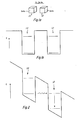
- FIG. 1 A simplified sample embodiment, which demonstrates some of the key principles of operation used in the present invention, is shown in Figure 1.
- Separate wells of gallium arsenide are embedded in a matrix of aluminum gallium arsenide.
- the bandgap of AIGaAs is wider than that of GaAs.
- the pseudo-binary alloys of the formula Al x Ga 1 -xAs are all semiconductors, with a bandgap which increases as a function of x).
- This different bandgap means that conduction- band electrons in the lattice see a lower potential energy in the GaAs regions than in the AIGaAs regions.
- a particular advantage of this material system is that the interface between GaAs and AIGaAs is a very well behaved one, that is such interfaces can be fabricated with an extremely low density of surface states (less than the Si/Si0 2 interface), and can preserve lattice match almost perfectly between the GaAs and the AIGaAs sides of the interface.
- the present invention can be practiced with a wide variety of material systems, and not only semiconductors.
- the wells 10 are about 125 angstroms wide, and the spacing between the wells is also about 125 angstroms.
- the dimensions of these wells are small enough that the energy states of electrons in the well will be quantized. That is, these well are preferably made cubic, and the allowable energy states of an electron in a cubic well of such dimensions can be calculated easily, using the effective mass approximation for the behavior of the electron, as a simple particle in a box problem in quantum mechanics.
- each energy level in such a quantized system is strictly limited. That is, the lowest lying energy level in each well in this example can be populated by only two electrons, the next level up can be populated by only six electrons, the new level up can be populated by only ten electrons, and so on.
- This means that the number of carriers within a well is strictly limited. Thus, a carrier cannot tunnel to an energy state in the next well if that energy state is already completely filled.
- each well can hold only a few carriers at a time, it should be noted that the transition times are expressly short (typically far less than a pico-second), and total current can be increased by operating many pairs of wells in parallel.
- the wells are placed sufficiently close such that the probability density of an electron in one well extends into the neighboring well; that is, the wells 10 and 12 in Figure 1 are close enough together that electrons can tunnel between them easily.
- an electron in the first well can tunnel easily to a state of equal energy in the second well, but of course it cannot do this unless an unoccupied state have the same energy actually exists in the second well.
- the energy levels in the two wells do not line up.
- an electron in the first well can only tunnel to states of the second well which have a different energy than the first well, and it can only tunnel to such states if there is also some mechanism whereby the electron can lose or gain enough energy to reach the energy of the lower lying available state in the second well.
- the chief mechanism for the changing of the energy of an electron to achieve tunnelling in this fashion is relaxation via surface states. That is, even the GaAs to AIGaAs interface, which is exceedingly benign as semiconductor interfaces go, will have a measurable density of surface states at the interface. Such surface states provide a scattering process which will permit an electron to transfer to higher or lower energy, if it intersects one of the available sites for scattering. That is, the interface can be described as having an areal density of scattering sites which are capable of changing the energy from an electron so that it can make the transition between wells even when the energy levels of the wells do not line up. This mode of transition is known as inelastic tunneling.
- the alternative mode of tunneling wherein the electron tunnels from the first well to the second with no change in energy, is known as resonant tunneling.
- Tunneling requires conservation both of energy and also of momentum.
- Momentum is also quantized for small potential wells. That is, in each dimension of the box which defines the boundaries of the potential well, the smaller the length of that dimension the more widely spaced the allowable values of that component of momentum will be.
- resonant tunneling can occur between two very closely spaced thin sheets of lower potential. Since the potential wells are very large in two dimensions, the momentum components in those two dimensions are not quantized. That is, when one dimension of a potential well is large, the momentum components in that direction are so closely spaced that a background lattice phonon will be available to supply the momentum difference.
- the density of phonons found in the lattice follows Bose-Einstein statics, i.e. the number of phonons found in the lattice at energy E in a background lattice temperature T varies as 1 over (EXP ((E/ kT)-1)).
- This energy distribution of phonons also implys a distribution for the magnitude of momentum of the phonons, and, since the phonons can be treated as approximately isotropic in reasonable semiconductor materials, this same distribution also specifies the distribution of phonons having a desired value of some one particular component of momentum.
- the quantization of momentum in a potential well can be considered as discrete or quazi-continuous only in relation to temperature.
- the resonant tunneling gain is enhanced in accordance with the number of parameters which must be met.
- all three components of momentum and therefore energy
- the chances of it finding a lattice phonon which has exactly the right components to satisfy the difference in each of the three momentum values is quite small. However, if only one component must be adjusted, the chances of accidentally doing this by interaction of the lattice phonon are much greater.
- the preferred embodiments of the present invention use structures wherein all three components of momentum are quantized.
- a class of less preferred alternative embodiments of the present invention uses structures wherein only two components of momentum but not energy are quantized, i.e. closely spaced thin wires. It is easy to satisfy the momentum constraint alone by a phonon-assisted process, but the necessity for satisfying both energy and momentum conversation is what keeps the rate for inelastic tunneling background controlled. That is, if a scattering center at the metallurgical interface can change the energy of a carrier, it is easy for one of the lattice phonons to provide the appropriate adjustment in momentum.
- the separation of the quantized energy states in a well increases as the well dimension becomes smaller.
- the rate of tunneling is increased. That is, the probability of tunneling can be expressed as a constant times exp(-2dxf(E)), where d is the distance between the wells and E is the energy difference.
- thermal "smearing” i.e. redistribution of energy level populations caused by background thermal energy. That is, the density of states distribution within each well of the discrete energy levels is broadened somewhat by thermal smearing. At higher temperatures, the thermal smearing is greater. The problem thermal smearing causes is that the operating temperature must be low enough that thermal smearing does not populate higher energy level states. That is, the electrons should reside in the lowest energy level to eliminate accidental coincidences and bidirectional elastic tunneling. This reduces to the condition that the energy spacing must be much larger than the thermal energy of the electrons. Thus, for operation at 4°K with GaAs wells in an Al. 3 Ga.
- the well width (and well spacing) should be in the neighborhood of .1 to .2 microns or less.
- the critical dimension needs to be reduced merely to a number on the order of 12.5 nm (125 Angstroms) or less.
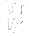
- the energy levels in adjacent wells can be made to line up or not line up simply by applying a bias, as shown in Figure 2.
- a bias voltage has been applied in the direction of conduction, so that the second level in the second well is lined up with the - first level in the first well. Under these conditions resonant tunneling will regularly occur, and the fast relaxation from the second level to the ground state in the second well ensures that the device is unidirectional.
- the frequency of inelastic transitions is limited by the density of available scattering sites.
- the density of scattering sites is in effect an areal density, since it arises primarily from surface states rather than from bulk defects or particles within the crystal lattice.
- the limiting factor is a areal density of defects, the inelastic tunneling current is relatively insensitive to the distance between wells. This means that, for good quality material, as the dimensions are scaled the resonant tunneling current increases tremendously, but the inelastic tunneling current does not increase much.
- the lifetime for relaxation from a higher lying state to an empty lower state will typically be much shorter than the typical time for tunneling.
- a higher level which has been excited in any fashion will tend to relax to the depleted lower level much faster than it will tunnel.
- empty lower levels exist below the higher level from which tunneling is possible. This imposes a constraint on the input contact, which will now be discussed.
- Figure 6 shows the energy diagrams for a system of two coupled wells 10 and 12 plus input and output contacts 14 and 16.
- the input and output contacts are doped, although the wells and the areas between them are preferably not.
- two important limitations on the well size arise from the necessities of making input contact and output contact.
- the input contact will fill all levels of the first well 10 by tunneling, up to an energy approximately equal to the Fermi level of the electrons in the doped semiconductor which provides the input contact. This means that none of the levels thus still filled up must line up with levels in the second well when tunneling is not desired. That is, if the well are too large, they will have discrete energy states at the bottom of the well but will include densely spaced states below the Fermi level of the input contact.
- the number of states in each well will be small, e.g. 4 states perwell. With such a small number of states, there will be bias conditions under which no actual line ups exist.
- Each tunneling transition described above is a transition of only a limited number of electrons for each pair of coincidental states. That is, each of the discrete energy levels in the quantum well can be populated by only a certain definite number of electrons. In the example discussed above, wherein the energy well has the approximate physical shape of a cube, the lowest lying level can be populated by only two electrons, and no more. The next higher energy level can be populated by only six electrons, and no more. The third energy level can be populated by only 12 electrons, and no more. Most of the higher-lying levels can also be populated by only 12, although some may have a higher maximum occupancy because of accidental degeneracies.
- the multiple states at each allowable energy level are distinguished by other quantum numbers. That is, for example, the six electrons in a second energy level can have one of two possible states of spin, and can have one of three possible momentum vector directions. However, this distinction among isoenergetic states is relatively unimportant for understanding the present invention.
- each tunneling transition can transport up to a dozen carriers for each pair of lined-up wells. More than one pair of wells may be lined up at the same time. Moreover, many pairs of wells may be operated in parallel. Moreover, the transit time for tunneling can be extremely small, less than a pico second. Thus, although only a few electrons are translated in each tunneling event, a reasonable current density can be achieved nevertheless.
- a basic family of embodiments is structures, as described above, wherein two quantized wells separate an input contact from an output contact.
- further aspect of the present invention provide numerous other kinds of innonative device structures.
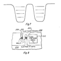
- a three terminal device is shown in a plan view in Figure 8.
- a first quantum dot 202 is coupled to a second quantum dot 204, which is coupled to an output contact 210.
- the dimensions of the quantum dots 202 and 204 are selected as discussed above for quantum wells, but the output contact 210 is made sufficiently large that a quasi-continuum of states is available.
- the quantum well 202 is coupled from beneath to an electrode 206, and the quantum well 204 is coupled from beneath an electrode 208. These are preferably degenerately doped semiconductor regions, or may be metal lines, but in any case provide the long-distance routing necessary for formation of conventional electronic circuits.
- the quantum wells 202 and 204 have only 2 components of momentum discretely quantized, since they are directly connected to their respective electrodes. That is, the electrodes 206 and 208 can be, for example, tungsten, with a thin layer of a conventional barrier metallization optionally provided on top.
- the GaAs of quantum wells 202 and 204 are formed directly on top of this conductor.
- the electrodes 206 and 208 are n+ GaAs.
- a thin barrier of AIGaAs can be provided beneath each of the quantum wells 202 or 204 and above the respective contact 206 or 208.
- This barrier is sufficiently thin that it is readily tunneled through, and therefore does not prevent DC coupling of each quantum well to its respective electrode, but even this thin a barrier would be sufficiently small to provide sufficient quantization of all 3 parameters of momentum within each of the wells 202 and 204, and thereby increase the relative resonant tunneling gain at the expense of a small increase in processing complexity and small dscrease in overall current.
- FIG. 9 A larger scale version of essentially this structure is shown in Figure 9.
- This 3-terminal quantum well device can be configured with multiple chains of quantum well pairs 202, 204 in parallel, for greater current flow.
- electrode 206 can be thoought of as acting as a source
- electrode 208 can be thought of as a gate electrode
- electrode 210 can be thought of as a drain electrode.
- Pattern 213 can be used to define the well locations 202 and 204.
- Figure 10 shows a cross section of this structure, including ground plane 211.
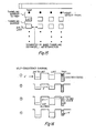
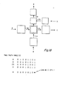
- FIG. 11 A further variation of this structure is shown in Figure 11. Note that additional electrodes 208 prime are used to provide longer chains of wells 202, 204 prime, 204 prime, etc., wherein resonant tunneling will occur only if the voltages on all of the electrodes 206 and 208 prime jointly satisfy one single condition (or some one of a small set of conditions). That is, Figure 12 shows a sample set of electrode bias conditions wherein resonant tunneling will occur, and Figure 13 shows a different set of bias conditions wherein resonant tunneling will not occur.
- This multiple-gate device is particularly useful for a read only memory.
- ROM read only memory
- information is hard-programmed simply by changing the degree of electrical coupling of a column line to underlying quantum wells.
- a sample of this embodiment is shown in Figure 14.
- a particular advantage of this embodiment is that the patterning of the metal lines need not be exactly aligned to the pattern of the underlying quantum wells. That is, if the pitch of the metal lines can be made twice or more that of the quantum wells, and the ROM will still function.
- column lines 302, 304, 306, etc. are overlying metal lines.
- Column line 302 is electrically coupled to row 310 of quantum wells, but not coupled (or less well coupled) to row 312 of quantum wells. This differential coupling can be accomplished by holes cut in a field plate, or by a dielectric patterned in multiple thicknesses.
- a sample mode of operation of this structure as follows: A background potential is defined for every column (i.e., all columns fixed at ground) such that resonant tunneling occurs through each row of quantum devices 310, 312, etc. When it is desired to read out a column of cells, the column line 302 for that column is changed to some different voltage.
- FIG. 21-36 A sample process for fabricating quantum well devices according to the present invention (Fig. 21-36) will now be described. In particular, fabrication of 3-terminal devices, as discussed above, will be used as an example.
- the beginning material is a semi-insulating GaAs substrate with 2 epitaxial layers.
- the substrate is preferably chromium doped, e.g. to 10 15 per cubic centimeter, although this is not necessary.
- the first epitaxial layer is n+ GaAs. This layer will provide connections, and is therefore fairly thick and of a fairly high conductivity, e.g. 500 nm (5000 angstroms) thick and doped to lo l8 per cubic centimeter or more n type. On top of this is deposited the thin lightly doped n-type layer which will patterned to form the actual quantum wells.
- This layer is doped, e.g., about lo l6 per cubic centimeter n-type, and, in a sample embodiment, is 15 nm (150 angstroms) thick. (The light doping is used merely so that some carriers are available. Heavier doping would increase inelastic tunneling).
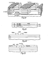
- Figure 21 shows an initial structure, having epitaxial layers 404 and 406 atop substrate 402.
- an extremely thin layer of AIGaAs could be interposed between layers 404 and 406.
- This structure is preferably fabricated by molecular beam epitaxy, to provide the desired sharp doping transitions, but this is not strictly necessary. Published chemical vapor deposition results, particularly using organo metallic CVD (MOCVD), also state results of extremely sharp transitions.
- MOCVD organo metallic CVD
- the first patterning step follows.
- patterning is done using electron beam with an E beam resist such as PMMA (polymethylmethacrylate).
- PMMA polymethylmethacrylate
- Figure 22 shows the epitaxial structure of Figure 21, with a patterned layer of PMMA 408 (patterned by e-beam writing and developing) in place.
- a reactive ion etching (RIE) mask material is then deposited.
- RIE reactive ion etching
- an aluminum layer 410 and a gold/germanium/nickel layer 412 are used for this, The pattern layer 408 is then lifted off, to expose only selected fine line portions of the epitaxial layer 406, as seen in Figure 23.
- Reactive ion etching is now conventionally performed to cut trenches 414 through the epitaxial layer 406 and 404 down into the substrate 402.
- RIE conditions are conventionally known for such patterning, and extreme anistropy is readily achieved at low pressure, at the expense of somewhat slow etching.
- the aluminum layer 410 is removed in dilute HCI to remove the RIE masking layer 410 and 412, as seen in Figure 25.
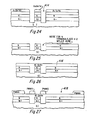
- an AIGaAs layer 416 is epitaxially regrown overall. This fills the trenches 414. It is preferable to perform this regrowth using molecular beam epitaxy. However, again, metal organic CVD is an alternative technology. However, in any case, it is important that this regrowth be of extremely high quality, since the sidewall interface between the GaAs wells formed from layer 406 and the AIGaAs fill 416 are extremely critical, as discussed above. This regrown structure shown in Figure 26.
- a second patterning step is performed.
- the pattern used in this case is essentially the same pattern over the wells, but also includes, the output contact in the finished structure.
- This pattern, seen in Figure 27, is converted to a hard mask pattern, seen in Figure 28, which is then reactive ion etched again.
- this reactive ion etching step has a critical depth control. It must be continued to etch into, but not through, the n+ layer 404. This critical depth control provides one reason for making the n+ layer 404 so thick, as discussed above.
- the masking metal is stripped (Figure 30), and AIGaAs is regrown overall.
- the AIGaAs needs to have a high enough percentage of aluminum to impose a significantly different conduction band energy between the AIGaAs and GaAs, but it is preferable that the aluminum percentage not be too high, to provide for the best possible GaAs to AIGaAs interface.
- a composition of about A[ 0 . 3 Ga O . 7 As is used.
- Figure 31 shows the resulting structure, with the new AIGaAs layer 420. Note that, in Figure 30, some portions of the AIGaAs layer 416 survive, and these portions are incorporated in the layer 420. Again, the layer 420 must be epitaxial grown with extremely good interface quality.
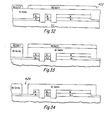
- a contact metallization pattern is then applied, as shown in Figure 32.
- the geometries are less demanding at this step and optical resist 422 with optical patterning is preferably used.
- a selective etch is then used, which will etch through AIGaAs and stop on n+ GaAs. Hydrogen fluoride has this property.
- This step provides contact holes 424, as seen in Figure 34.
- Metallization patterning is then applied, again preferably using an optical resist 426, as seen in Figure 35, and metal (such as AuGe/Ni) is then deposited, e.g. by evaporation, and lift off patterned, resulting in the structure as shown in Figure 36.
- a very similar fabrication technique can be used to fabricate quantum well array structure, e.g. from ROMs, simply by performing the second patterning step (shown in Figure 27) to define linear patterns at right angles to linear patterns defined by the first patterning step, so that the intersection of the two defines locations of the quantum well dots.
- a basic difficulty in interconnecting quantum well devices according to the present invention to form random logic circuit is their electrical characteristics. These devices may be considered to have very high input impedance and very low output impedance.
- a circuit structure for output coupling is described which permits the output of quantum well devices according to the present invention to switch macroscopic currents, i.e. currents comparable to those normally used in integrated circuit wiring. These macroscopic currents can then be used to change electric potentials and thereby switch further stages of quantum well devices.
- This effect need not be limited to wires of such small dimension.
- the resistance of a larger wire can be similarly modulated.
- a dielectric with traps coated over the surface of the wire can substantially modulate the wires resistance as the traps are populated and depopulated.
- a field plate is prefer- baly used, which provides a bias normal to the surface of the wire.
- the dimensions of the wire next to the scattering site must be such that the wire is in what is known as the Anderson localization regime: the wave function of the electron must significantly overlap the entire periphery of the wire, i.e. all four faces of a square wire. In this regime, the resistance will be extremely sensitive to surface states adjacent to the wire. There will typically be many unintentionally generated surface states, but these normally have low activation energy.
- the operating temperature is selected so that these unwanted surface states will boil off readily, i.e., selected such that kT is comparable to or larger than the activation energy of these parasitic surface states, but such that the activation energy of the surface states in which charges to be trapped to effect modulation is more than several times as much as kT.
- the principle application of this output amplifier stage is believed to be for devices operating at temperatures in the neighborhood of 77 Kelvin, i.e. liquid nitrogen temperatures.
- higher operating temperatures can be used if carriers can be injected into deeper surface states.
- the surface states used in the presently preferred embodiment are about 20 to 30 meV or more removed from the conduction band energy of the metal.
- Operation in the Anderson localization regime means that the dimensions of the wire close to the scattering center cannot possibly be greater than 50x50 nm (500x500 angstroms), and are preferably closer to 10x10 nm (100x100 angstroms).
- the resistance of the wire is roughly 100 K to one megohm per micron.
- Each scattering center which is populated or depopulated can impose a resistance change of a percent or so, and by using several such scattering centers, a total resistance change of 5% or so is achieved.
- these metal lines are used in pairs, and a change in current of a few percent is easily enough to trip a conventional sense amplifier.
- the presently preferred embodiment for accomplishing carrier injection into these traps is to have the trapping site connected to the last well in a chain of quantum wells by tunneling, i.e., the separation from the trapping site to the last well in the chain should be removed from the trapping site by no more than a few times the distance between wells, and preferably less.
- Tunneling out of the trap into the last well is not a limitation in the preferred embodiment since the electron enters the trap through excited states.
- the reverse tunneling is only inelastic. However, for a sufficiently deep trap, the required phonon energy becomes so large that the inelastic tunneling is negligible.
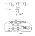
- the trapping site can be written with extreme precision using a focused ion beam. Thus, the configuration of this output stage is shown in Fig. 15.
- one-way well coupling is optionally used to assist injection of carriers into these traps, to modulate the metal lines resistance.
- This one-way coupling is made possible by the self-consistent tunneling effects of the wells. That is, in addition to the factors discussed above, the presence or absence of electrons in the wells will itself modulate the electric field between wells. Thus, as shown in Figs. 16 A and B, the change in electric field caused by the presence of an additional carrier in a second well can itself be sufficient to forbid tunneling.
- a carrier will readily tunnel from well 1 into a depleted level in well 2, but that same carrier cannot tunnel back into well 1 except through inelastic channels, because now the levels no longer line up.
- the well dimensions should preferably be smaller than those necessary, at the operating temperature, or any resonant tunneling gain.
- wells of appropriate dimensions for operation at room temperature will show such effects if operated at 77K or at 4K.
- the smaller wells mean that the field generated by the potential shift caused by the addition of one carrier will be greater.
- a field plate or other bias connection is used to define a reference voltage V o for well 3.
- the wells are tailored such that tunneling occurs from well 1 to well 3 only when V 3 equals V o ; tunneling occurs from well 2 to well 3 only when V 3 equals V o plus E, i.e., when the potential of well 3 has been modified by the presence of one electron; tunneling occurs from well 3 to well 4 only when well 3 has a potential V 3 equals V o plus 2e.
- Input Signal A supplies carriers tunneling into well 1
- input-signal B supplies carriers tunneling into well 2
- an output contact retrieves an output signal C from well 4.
- Boolean primitives are easily created. For example, in the same layout of wells, if we redefine the well couplings such that the tunneling occurs from well 1 to well 3 when V 3 equals V o , from well 2 to well 3 when V 3 equals V o , and from well 3 to well 4 when V 3 equals V o plus E, we now have an OR gate. These couplings can be used to configure all primitive Boolean algebraic logic cells and more. In this regime, where self-generated fields are sufficient to disrupt tunneling, a problem may be caused by the presence of excess carriers in a well.
- a further family of the embodiments of the present invention utilize vertical tunneling.
- An attraction of such structures is that extremely small dimensions, with extremely good interface quality are easier to achieve in the vertical dimension then in the lateral dimension.
- this spacing of energy states in the well is in general defined by the volume of the well.
- the well may be configured as a thin flat box rather than a roughly cubic box.
- two of the momentum components would be quantized with extremely closedly spaced values, and the third component would be quantized with extremely widely spaced allowable momentum values.
- the wells 604-608 are preferably made of a first semiconductor and the barrier medium 612 is preferably made of a second, wider-band gap semiconductor.
- Gallium arsenide and AIGaAs are preferable for these two semiconductors.
- the present invention provides the above- mentioned objects, as well as numerous other technical advantages in accordance with the foregoing description.
- the present invention is a pioneering invention, and can be modified with an immense variety of modification and variations.
- Si wells can be used in an Si0 2 barrier medium, or other semiconductor/ semiconductor or semiconductor/insulator systems can be used, in place of the preferred GaAs/AIGaAs materials system.
- the scope of the present invention is not limited except as set forth in the accompanying claims.
Landscapes
- Engineering & Computer Science (AREA)
- Chemical & Material Sciences (AREA)
- Nanotechnology (AREA)
- Physics & Mathematics (AREA)
- Mathematical Physics (AREA)
- Theoretical Computer Science (AREA)
- Crystallography & Structural Chemistry (AREA)
- Bipolar Transistors (AREA)
- Semiconductor Memories (AREA)
- Junction Field-Effect Transistors (AREA)
Claims (14)
Applications Claiming Priority (2)
| Application Number | Priority Date | Filing Date | Title |
|---|---|---|---|
| US62680284A | 1984-07-02 | 1984-07-02 | |
| US626802 | 1984-07-02 |
Publications (3)
| Publication Number | Publication Date |
|---|---|
| EP0170044A2 EP0170044A2 (de) | 1986-02-05 |
| EP0170044A3 EP0170044A3 (en) | 1987-08-19 |
| EP0170044B1 true EP0170044B1 (de) | 1989-11-02 |
Family
ID=24511915
Family Applications (1)
| Application Number | Title | Priority Date | Filing Date |
|---|---|---|---|
| EP85107785A Expired EP0170044B1 (de) | 1984-07-02 | 1985-06-24 | Quantengekoppelte Bauelemente |
Country Status (3)
| Country | Link |
|---|---|
| EP (1) | EP0170044B1 (de) |
| JP (1) | JPS6182473A (de) |
| DE (1) | DE3574082D1 (de) |
Families Citing this family (6)
| Publication number | Priority date | Publication date | Assignee | Title |
|---|---|---|---|---|
| JP2690922B2 (ja) * | 1987-12-25 | 1997-12-17 | 株式会社日立製作所 | 共鳴トンネリング素子 |
| JPH0779158B2 (ja) * | 1988-11-19 | 1995-08-23 | 新技術事業団 | 結合量子箱列構造半導体 |
| GB2256313B (en) * | 1991-01-04 | 1995-03-29 | Hitachi Europ Ltd | Semiconductor device |
| JP3243303B2 (ja) * | 1991-10-28 | 2002-01-07 | ゼロックス・コーポレーション | 量子閉じ込め半導体発光素子及びその製造方法 |
| US5283445A (en) * | 1991-11-29 | 1994-02-01 | Fujitsu Limited | Quantum semiconductor device employing quantum boxes for enabling compact size and high-speed operation |
| EP0588062B1 (de) * | 1992-08-13 | 1996-03-20 | Sony Corporation | Quantenbauelement und dessen Herstellungsverfahren |
Family Cites Families (1)
| Publication number | Priority date | Publication date | Assignee | Title |
|---|---|---|---|---|
| FR2504732A1 (fr) * | 1981-04-27 | 1982-10-29 | Thomson Csf | Transistor tunnel a double heterojonction |
-
1985
- 1985-06-24 DE DE8585107785T patent/DE3574082D1/de not_active Expired
- 1985-06-24 EP EP85107785A patent/EP0170044B1/de not_active Expired
- 1985-07-02 JP JP60144116A patent/JPS6182473A/ja active Pending
Also Published As
| Publication number | Publication date |
|---|---|
| JPS6182473A (ja) | 1986-04-26 |
| EP0170044A3 (en) | 1987-08-19 |
| DE3574082D1 (en) | 1989-12-07 |
| EP0170044A2 (de) | 1986-02-05 |
Similar Documents
| Publication | Publication Date | Title |
|---|---|---|
| US4575924A (en) | Process for fabricating quantum-well devices utilizing etch and refill techniques | |
| US4581621A (en) | Quantum device output switch | |
| US4912531A (en) | Three-terminal quantum device | |
| US5032877A (en) | Quantum-coupled ROM | |
| US4783427A (en) | Process for fabricating quantum-well devices | |
| US4503447A (en) | Multi-dimensional quantum well device | |
| US6498354B1 (en) | Single charge carrier transistor, method of holding a charge carrier within a quantum dot, and method of detection | |
| US5432362A (en) | Resonant tunnel effect quantum well transistor | |
| US5234848A (en) | Method for fabricating lateral resonant tunneling transistor with heterojunction barriers | |
| EP0042489B1 (de) | Halbleiterbauelemente und Anwendung dieser Bauelemente | |
| US4721983A (en) | Three terminal tunneling device | |
| US4799091A (en) | Quantum device output switch | |
| JPH0732250B2 (ja) | 半導体デバイス | |
| US4959696A (en) | Three terminal tunneling device and method | |
| US4872038A (en) | Lateral surface superlattice having negative differential conductivity novel process for producing same | |
| US4969018A (en) | Quantum-well logic using self-generated potentials | |
| EP0170044B1 (de) | Quantengekoppelte Bauelemente | |
| EP0216155A2 (de) | Tunneleffektbauelement mit drei Polen | |
| US5346851A (en) | Method of fabricating Shannon Cell circuits | |
| Kano et al. | Negative differential resistance device built in a biwell GaAs/AlGaAs superlattice | |
| JPS61123174A (ja) | 垂直量子ウエル装置 | |
| JP4007560B2 (ja) | 半導体装置 | |
| Iafrate | US Army Electronics Technology and Devices Laboratory (ERADCOM) Fort Monmouth, New Jersey 07703 | |
| Kelly | A second decade of semiconductor heterojunction devices | |
| Beltram et al. | Artificial semiconductor structures: Electronic properties and device applications |
Legal Events
| Date | Code | Title | Description |
|---|---|---|---|
| PUAI | Public reference made under article 153(3) epc to a published international application that has entered the european phase |
Free format text: ORIGINAL CODE: 0009012 |
|
| AK | Designated contracting states |
Designated state(s): DE FR GB |
|
| PUAL | Search report despatched |
Free format text: ORIGINAL CODE: 0009013 |
|
| AK | Designated contracting states |
Kind code of ref document: A3 Designated state(s): DE FR GB |
|
| 17P | Request for examination filed |
Effective date: 19880215 |
|
| 17Q | First examination report despatched |
Effective date: 19880727 |
|
| GRAA | (expected) grant |
Free format text: ORIGINAL CODE: 0009210 |
|
| AK | Designated contracting states |
Kind code of ref document: B1 Designated state(s): DE FR GB |
|
| PG25 | Lapsed in a contracting state [announced via postgrant information from national office to epo] |
Ref country code: FR Free format text: THE PATENT HAS BEEN ANNULLED BY A DECISION OF A NATIONAL AUTHORITY Effective date: 19891102 |
|
| REF | Corresponds to: |
Ref document number: 3574082 Country of ref document: DE Date of ref document: 19891207 |
|
| EN | Fr: translation not filed | ||
| PLBE | No opposition filed within time limit |
Free format text: ORIGINAL CODE: 0009261 |
|
| STAA | Information on the status of an ep patent application or granted ep patent |
Free format text: STATUS: NO OPPOSITION FILED WITHIN TIME LIMIT |
|
| 26N | No opposition filed | ||
| PGFP | Annual fee paid to national office [announced via postgrant information from national office to epo] |
Ref country code: GB Payment date: 20010502 Year of fee payment: 17 |
|
| PGFP | Annual fee paid to national office [announced via postgrant information from national office to epo] |
Ref country code: DE Payment date: 20010627 Year of fee payment: 17 |
|
| REG | Reference to a national code |
Ref country code: GB Ref legal event code: IF02 |
|
| PG25 | Lapsed in a contracting state [announced via postgrant information from national office to epo] |
Ref country code: GB Free format text: LAPSE BECAUSE OF NON-PAYMENT OF DUE FEES Effective date: 20020624 |
|
| PG25 | Lapsed in a contracting state [announced via postgrant information from national office to epo] |
Ref country code: DE Free format text: LAPSE BECAUSE OF NON-PAYMENT OF DUE FEES Effective date: 20030101 |
|
| GBPC | Gb: european patent ceased through non-payment of renewal fee |
Effective date: 20020624 |