EP0170134A1 - Circuit logique utilisant des diodes Schottky et des transistors à effet de champ - Google Patents
Circuit logique utilisant des diodes Schottky et des transistors à effet de champ Download PDFInfo
- Publication number
- EP0170134A1 EP0170134A1 EP85108714A EP85108714A EP0170134A1 EP 0170134 A1 EP0170134 A1 EP 0170134A1 EP 85108714 A EP85108714 A EP 85108714A EP 85108714 A EP85108714 A EP 85108714A EP 0170134 A1 EP0170134 A1 EP 0170134A1
- Authority
- EP
- European Patent Office
- Prior art keywords
- node
- electrically connected
- circuit
- schottky diode
- logic
- Prior art date
- Legal status (The legal status is an assumption and is not a legal conclusion. Google has not performed a legal analysis and makes no representation as to the accuracy of the status listed.)
- Granted
Links
- 230000005669 field effect Effects 0.000 title claims abstract description 11
- 239000000758 substrate Substances 0.000 claims abstract description 17
- JBRZTFJDHDCESZ-UHFFFAOYSA-N AsGa Chemical compound [As]#[Ga] JBRZTFJDHDCESZ-UHFFFAOYSA-N 0.000 claims abstract description 11
- GPXJNWSHGFTCBW-UHFFFAOYSA-N Indium phosphide Chemical compound [In]#P GPXJNWSHGFTCBW-UHFFFAOYSA-N 0.000 claims abstract description 5
- 239000004065 semiconductor Substances 0.000 claims abstract description 5
- 239000007787 solid Substances 0.000 claims description 4
- 229910052751 metal Inorganic materials 0.000 claims 6
- 239000002184 metal Substances 0.000 claims 6
- 230000010354 integration Effects 0.000 abstract 1
- 229910001218 Gallium arsenide Inorganic materials 0.000 description 8
- 230000008901 benefit Effects 0.000 description 5
- 239000003990 capacitor Substances 0.000 description 5
- 230000004044 response Effects 0.000 description 3
- 230000000295 complement effect Effects 0.000 description 2
- 230000003068 static effect Effects 0.000 description 2
- 230000008859 change Effects 0.000 description 1
- 238000004590 computer program Methods 0.000 description 1
- 230000008878 coupling Effects 0.000 description 1
- 238000010168 coupling process Methods 0.000 description 1
- 238000005859 coupling reaction Methods 0.000 description 1
- 230000000593 degrading effect Effects 0.000 description 1
- 238000007599 discharging Methods 0.000 description 1
- 230000000694 effects Effects 0.000 description 1
- 238000005516 engineering process Methods 0.000 description 1
- 239000000463 material Substances 0.000 description 1
- 229910052710 silicon Inorganic materials 0.000 description 1
- 239000010703 silicon Substances 0.000 description 1
- 238000004088 simulation Methods 0.000 description 1
- 235000013599 spices Nutrition 0.000 description 1
Images

Classifications
-
- H—ELECTRICITY
- H03—ELECTRONIC CIRCUITRY
- H03K—PULSE TECHNIQUE
- H03K19/00—Logic circuits, i.e. having at least two inputs acting on one output; Inverting circuits
- H03K19/01—Modifications for accelerating switching
- H03K19/017—Modifications for accelerating switching in field-effect transistor circuits
- H03K19/01707—Modifications for accelerating switching in field-effect transistor circuits in asynchronous circuits
-
- H—ELECTRICITY
- H03—ELECTRONIC CIRCUITRY
- H03K—PULSE TECHNIQUE
- H03K19/00—Logic circuits, i.e. having at least two inputs acting on one output; Inverting circuits
- H03K19/02—Logic circuits, i.e. having at least two inputs acting on one output; Inverting circuits using specified components
- H03K19/08—Logic circuits, i.e. having at least two inputs acting on one output; Inverting circuits using specified components using semiconductor devices
- H03K19/094—Logic circuits, i.e. having at least two inputs acting on one output; Inverting circuits using specified components using semiconductor devices using field-effect transistors
- H03K19/0956—Schottky diode FET logic
Definitions
- This invention relates to integrated logic circuits wherein diodes serve as the nonlinear logic elements and field effect transistors (FETs) are switched in response to current flowing through the diodes.
- the invention particularly relates to such logic circuits wherein the substrate is a solid with high electron mobility such as gallium arsenide (GaAs), or indium phosphide (InP) the diodes are Schottky diodes
- SDFL Schottky diode field effect transistor logic
- the basic SDFL NOR logic circuit is shown in Figure 1.
- Schottky diode logic elements 12 and 14 are rendered conductive or nonconductive depending on logic inputs signals A and B. If at least one of diodes 12 or 14 are conducting, FET 16 is turned on which allows current to flow through an electrical load (e.g., pull up FET 18) and thereby affect the logic condition of the output 20.
- Voltage level shifting diodes, such as diode 22 are employed to allow the use of switching FETs with higher pinch-off voltages.
- FET 24 serves as a current source for biasing Schottky diodes 12, 14 and 22. Depletion mode MESFETs are preferably employed due to the limits of present processing technology. With a GaAs substrate, SDFL provides a very fast logic circuit.
- FFSL feed-forward static logic
- FFSL uses a FET 28 as the nonlinear logic element and FET 28 in conjunction with an electrical load (e.g., pull up FET 30) serves to invert logic signals input at node 31.
- FFSL features a "feed-forward capacitor" (i.e., the depletion capacitance of reverse biased Schottky diode 32) connected between an inverting logic node 34 and a voltage shifter/driver circuit branch (i.e., FETs 36 and 38 and Schottky diodes 40, 42 and 44). High frequency signals are transmitted to the voltage shifter branch through the depletion capacitance of reverse biased diode 32, allowing for very fast switching of the next stage which is coupled to output 46.
- a feed-forward capacitor enhances design flexibility by allowing the gate width of the voltage shifting branch to be reduced relative to the gate width of a comparable voltage shifting branch in BFL without degrading speed performance. By reducing the gate width of the voltage shifting branch, power dissipation can be reduced.
- FFSL uses a FET as a nonlinear logic element. FETs require considerable chip area due to their relatively large size and, being a three terminal device, additional area to accommodate overcrossings necessitated by the three terminals.
- the invention is an integrated logic circuit having a logic input, a logic output and a solid substrate.
- Schottky diodes integral with the substrate are connected such that they pass substantial current only in opposite directions along separate circuit branches between first and second nodes.
- the logic input is electrically connected to the first node and the logic signal at the second node is inverted to generate the logic output.
- a means for reverse biasing the diodes of one of the branches and for forward biasing the diodes of the other branch is provided.
- the above indicated signal inversion is preferably accomplished by switching a depletion mode MESFET with a logic signal from the second node.
- the substrate is perferably a material with high electron mobility such as GaAs or InP.
- the basic circuit employing the invention is used as a building block to construct multiple input logic circuits.
- direct electrical connection means connected by way of a low resistance conductive path without other circuit components such as FET junctions, diodes, capacitors or inductors therebetween.
- Electrical connection includes the direct connections defined above but also includes coupling through other circuit components such as those described above.
- circuit 48 has a logic input 50, nodes 52 and 54 respectively, first Schottky diode 56, second Schottky diode 58, current source means (e.g., depletion mode, source-gate shorted MESFET 60), a switching transistor (preferably a depletion mode MESFET 62), an electrical load or drain current source (preferably source-gate shorted, depletion mode MESFET 64) and logic output 66.
- current source means e.g., depletion mode, source-gate shorted MESFET 60
- switching transistor preferably a depletion mode MESFET 62
- an electrical load or drain current source preferably source-gate shorted, depletion mode MESFET 64
- Logic input 50 and node 52 are directly electrically connected, therefore a direct electrical connection to node 52 is also a direct electrical connection to logic input 50. Functionally, node 52 can serve as the logic input.
- Schottky diode 56 has its anode directly electrically connected to node 52 and its cathode electrically connected (either directly or through an optional voltage level shifting means such as Schottky diode 68) to node 54.
- Schottky diode 58 has its cathode electrically connected to node 52 and its anode electrically connected to node 54. Diodes 56 and 58 are adapted to pass substantial current only in opposite directions between nodes 52 and 54.
- MESFET 60 has its drain connected to node 54. MESFET 60 in conjunction with negative voltage supply -V S S serve to bias Schottky diodes 56, 58 and 68.
- MESFET 62 has its gate electrically connected to node 54, its source grounded and the logic output is taken at its drain. Pull up FET 64 is connected between the drain of MESFET 62 and positive voltage supply +V oD .
- circuit 48 receives a digital logic input signal A at logic input 50.
- Schottky diodes 56 and 68 are always forward biased and Schottky diode 58 (a feed-reverse capacitor-diode) is always reverse biased.
- A e.g., logic 1
- the forward bias voltage on Schottky diodes 56 and 68 is such that the current flowing through these diodes in the forward direction is relatively large causing a significant voltage drop across MESFET 60. This raises the voltage at node 54, and thus output node 66 is pulled low resulting in a low (i.e., O) logic signal.
- A is low (i.e., logic O)
- the current flowing through Schottky diodes 56 and 68 is relatively low.
- the voltage at node 54 is low and output node 66 is pulled high resulting in a high (i.e. 1) logic signal.
- FETS 62 and 64 serve to invert the voltage signal at node 54 by switching FET 62 on if node 54 is high and switching FET 62 off if node 54 is low.
- the second advantage of the present invention over SDFL is also due to the depletion capacitance of reverse biased Schottky diode 58.
- the depletion capacitance of Schottky diode 58 charges to some extent.
- some portion of the charge accumulated on the capacitance of reverse biased Schottky diode 58 during the time when FET 62 is on will still be present when FET 62 is next switched on.
- This residual charge in effect precharges node 54 so that less of a voltage change is needed to switch FET 62 on than if Schottky diode 58 were not utilized.
- Figure 4 shows an OR/NAND gate 70 with two inputs A and B employing the present invention.
- feed-reverse capacitor-diodes are darkened.
- the first logic input 72 leads to Schottky diodes 74, 76 and 78 which are configured like the Schottky diodes in circuit 4 8 with FET 80 serving as the bias current source.
- the logic signal at node 82 switches FET 84.
- Second logic input 86 leads to Schottky diodes 88, 90 and 92, which again are configured like the Schottky diodes in circuit 48, with FET 94 serving as the bias current source.
- the logic signal at node 96 switches FET 97.
- FETs 84 and 97 are connected in series with the drain of FET 97 connected to the source of FET 84.
- the source of FET 97 is connected to ground.
- the drain of FET 84 is in turn connected in series with the source of pull up FET 98.
- the drain of pull up FET 98 is connected to the positive voltage supply + V D D -
- the AND function is performed on the inputs to the gates of FETS 84 and 97, and the combination of FETs 84, 97 and 98 invert the AND result.
- the net result of circuit 70 is to perform an OR/NAND operation. Additional inputs, each leading to a set of Schottky diodes, and additional FETs in series with FETs 84 and 97 can be used to increase the fan-in of circuit 70.
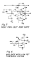
- Figure 5 displays a NOR gate 102 for high fan-out which employs the present invention.
- Circuit 102 is comprised of two portions.
- the first portion 104 is the basic NOR gate of Figure 3.
- the feed-reverse capacitor-diode in portion 104 is shown as diode 106.
- the second portion 108 increases the drive capability of portion 104 by feeding complement and true logic signals to the gates of FETs 110 and 112, respectively.
- FETs 110 and 112 are thus driven in complementary fashion and provide additional power as compared to circuit 48 of Figure 3.
- Schottky diode 114 is provided to lower the voltage level of node 1 16 (i.e., the logic output of portion 104) to accommodate the negative threshold voltage of depletion mode MESFET 110.
- a second feed-reverse capacitor-diode 118 is employed in circuit 102 to increase the switching speed of FET 110.
- Schottky diode 118 is electrically connected between nodes 116 and 120.
- FET 122 supplies bias current for diode 114.
- circuit 124 includes enhancement mode switching FET 126, nonlinear logic element Schottky diode 128, feed-reverse capacitor diode 130, a current bias source (e.g., resistor 132), pull up FET/load 134, input 136 and output 138.
- the threshold voltage of FET 126 is preferrably centered around O volts (e.g., -0.2v to 0.2v). This approach will result in a logic circuit which is more tolerant to threshold voltage variations than conventional enhancement direct coupled FET logic (DCFL).
- Additional diodes can be added to either circuit branch between nodes 52 and 54 in Figure 3.
- a forward biased diode (not shown) could be added in series with diodes 56 and 68 to further shift the voltage level of a logic signal.
- additional reverse biased diodes (not shown) could be added in series with diode 58, generally only one reverse biased diode will be used.
- the feed-reverse capacitance can be increased by simply using a larger reverse biased diode.
- circuit 4 8 of Figure 3 is advantageously configured with the depletion capacitance of Schottky diode 58 being three or four times larger than the total capacitance of the gates being driven. This is because the depletion capacitance of Schottky diode 58 and the load capacitance acts as a divider network.
- speed could be maintained at the level of SDFL with the current source and positive voltage supplies being reduced, thus reducing the power dissipated by the present invention as compared to SDFL.
- the present invention is preferably an integrated circuit having a solid substrate (not shown) with high electron mobility such as GaAs or InP.
- a solid substrate such as GaAs or InP.
- Other semiconductor substrates such as silicon, could of course also be used.
- MESFETS and Schottky diodes are the preferable circuit components since they are easily fabricated on GaAs.
- a further advantage of the present invention over SDFL is an extension of the range of frequency response.
- the basic SDFL circuit has a low pass filter response with an upper cut-off frequency, Inclusion of the feed-reverse capacitor-diode will increase the upper cut off frequency as compared to SDFL for equal loading of wire interconnect and fan-out. Also, for the same switching speed, power dissipation with SDFL employing a feed-reverse capacitor diode will be reduced as compared to SDFL without such a diode.
Landscapes
- Engineering & Computer Science (AREA)
- Physics & Mathematics (AREA)
- Computer Hardware Design (AREA)
- Computing Systems (AREA)
- General Engineering & Computer Science (AREA)
- Mathematical Physics (AREA)
- Power Engineering (AREA)
- Logic Circuits (AREA)
Applications Claiming Priority (2)
| Application Number | Priority Date | Filing Date | Title |
|---|---|---|---|
| US63235984A | 1984-07-19 | 1984-07-19 | |
| US632359 | 1984-07-19 |
Publications (2)
| Publication Number | Publication Date |
|---|---|
| EP0170134A1 true EP0170134A1 (fr) | 1986-02-05 |
| EP0170134B1 EP0170134B1 (fr) | 1989-02-08 |
Family
ID=24535212
Family Applications (1)
| Application Number | Title | Priority Date | Filing Date |
|---|---|---|---|
| EP19850108714 Expired EP0170134B1 (fr) | 1984-07-19 | 1985-07-12 | Circuit logique utilisant des diodes Schottky et des transistors à effet de champ |
Country Status (4)
| Country | Link |
|---|---|
| EP (1) | EP0170134B1 (fr) |
| JP (1) | JPS6139725A (fr) |
| CA (1) | CA1245304A (fr) |
| DE (1) | DE3568243D1 (fr) |
Cited By (4)
| Publication number | Priority date | Publication date | Assignee | Title |
|---|---|---|---|---|
| EP0167076A3 (en) * | 1984-06-27 | 1987-10-07 | Honeywell Inc. | Digital circuit using mesfets |
| US4701643A (en) * | 1986-03-24 | 1987-10-20 | Ford Microelectronics, Inc. | FET gate current limiter circuits |
| US4800303A (en) * | 1987-05-19 | 1989-01-24 | Gazelle Microcircuits, Inc. | TTL compatible output buffer |
| WO1989003137A1 (fr) * | 1987-10-02 | 1989-04-06 | Cray Research, Inc. | Systeme de configuration logique a l'arseniure de gallium |
Citations (3)
| Publication number | Priority date | Publication date | Assignee | Title |
|---|---|---|---|---|
| DD40592A (fr) * | ||||
| US4300064A (en) * | 1979-02-12 | 1981-11-10 | Rockwell International Corporation | Schottky diode FET logic integrated circuit |
| EP0075915A2 (fr) * | 1981-09-30 | 1983-04-06 | Kabushiki Kaisha Toshiba | Circuit logique pouvant être alimenté par une tension unique |
Family Cites Families (1)
| Publication number | Priority date | Publication date | Assignee | Title |
|---|---|---|---|---|
| JPS5862939A (ja) * | 1981-10-09 | 1983-04-14 | Hitachi Ltd | 論理回路 |
-
1985
- 1985-06-24 CA CA000484953A patent/CA1245304A/fr not_active Expired
- 1985-07-12 DE DE8585108714T patent/DE3568243D1/de not_active Expired
- 1985-07-12 EP EP19850108714 patent/EP0170134B1/fr not_active Expired
- 1985-07-18 JP JP15928685A patent/JPS6139725A/ja active Pending
Patent Citations (3)
| Publication number | Priority date | Publication date | Assignee | Title |
|---|---|---|---|---|
| DD40592A (fr) * | ||||
| US4300064A (en) * | 1979-02-12 | 1981-11-10 | Rockwell International Corporation | Schottky diode FET logic integrated circuit |
| EP0075915A2 (fr) * | 1981-09-30 | 1983-04-06 | Kabushiki Kaisha Toshiba | Circuit logique pouvant être alimenté par une tension unique |
Non-Patent Citations (4)
| Title |
|---|
| IEEE ELECTRON DEVICE LETTERS, vol. EDL-3, no. 9, September 1982, pages 264-267; New York, US; M.R. NAMORDI et al.: "A novel low-power static GaAs MESFET logic gate", * |
| IEEE JOURNAL OF SOLID-STATE CIRCUITS, vol. SC-19, no. 1, February 1984, pages 10-22; New York, US; T.T. VU et al.: "A gallium arsenide SDFL gate array with on-chip RAM" * |
| PATENT ABSTRACTS OF JAPAN, vol. 7, no. 154 (E-185)[1299], 6th July 1983; & JP-A-58 062 939 (HITACHI SEISAKUSHO K.K.) 14-04-1983 * |
| PATENT ABSTRACTS OF JAPAN, vol. 7, no. 17 (E-154)[1162], 22nd January 1983; & JP-A-57 176 837 (HITACHI SEISAKUSHO K.K.) 30-10-1982 * |
Cited By (6)
| Publication number | Priority date | Publication date | Assignee | Title |
|---|---|---|---|---|
| EP0167076A3 (en) * | 1984-06-27 | 1987-10-07 | Honeywell Inc. | Digital circuit using mesfets |
| US4701643A (en) * | 1986-03-24 | 1987-10-20 | Ford Microelectronics, Inc. | FET gate current limiter circuits |
| US4800303A (en) * | 1987-05-19 | 1989-01-24 | Gazelle Microcircuits, Inc. | TTL compatible output buffer |
| GB2208144A (en) * | 1987-05-19 | 1989-03-01 | Gazelle Microcircuits Inc | Ttl compatible buffer in compound semiconductor technology |
| GB2208144B (en) * | 1987-05-19 | 1992-01-22 | Gazelle Microcircuits Inc | Buffer circuit |
| WO1989003137A1 (fr) * | 1987-10-02 | 1989-04-06 | Cray Research, Inc. | Systeme de configuration logique a l'arseniure de gallium |
Also Published As
| Publication number | Publication date |
|---|---|
| EP0170134B1 (fr) | 1989-02-08 |
| JPS6139725A (ja) | 1986-02-25 |
| DE3568243D1 (en) | 1989-03-16 |
| CA1245304A (fr) | 1988-11-22 |
Similar Documents
| Publication | Publication Date | Title |
|---|---|---|
| EP0145004B1 (fr) | Circuit composite, transistors bipolaires-transistors à effet de champ | |
| EP0075915B1 (fr) | Circuit logique pouvant être alimenté par une tension unique | |
| JP2549141B2 (ja) | Bifet論理回路 | |
| EP0099100A1 (fr) | Circuit porte utilisant des transistors à effet de champ et des transistors bipolaires | |
| US4028556A (en) | High-speed, low consumption integrated logic circuit | |
| US4663543A (en) | Voltage level shifting depletion mode FET logical circuit | |
| US3573490A (en) | Capacitor pull-up reigister bit | |
| US4490632A (en) | Noninverting amplifier circuit for one propagation delay complex logic gates | |
| US4798979A (en) | Schottky diode logic for E-mode FET/D-mode FET VLSI circuits | |
| US4798972A (en) | Apparatus and method for capacitor coupled complementary buffering | |
| JPH0763140B2 (ja) | ゲ−ト回路 | |
| US4489246A (en) | Field effect transistor logic circuit having high operating speed and low power consumption | |
| EP0562719B1 (fr) | Dispositif de circuit intégré formé par un semiconducteur composé | |
| EP0170134B1 (fr) | Circuit logique utilisant des diodes Schottky et des transistors à effet de champ | |
| US4725743A (en) | Two-stage digital logic circuits including an input switching stage and an output driving stage incorporating gallium arsenide FET devices | |
| JPH0252460B2 (fr) | ||
| EP0196391B1 (fr) | Circuit intégré à réseau de portes logiques en arséniure de gallium comportant des portes NON-ET en logique à transistors à effet de champ à couplage direct | |
| EP0207429A2 (fr) | Circuit d'entrée pour logique FET | |
| US4885480A (en) | Source follower field-effect logic gate (SFFL) suitable for III-V technologies | |
| US5661411A (en) | Feedback controlled load logic circuit | |
| KR950000352B1 (ko) | 반도체 논리회로 | |
| US5343091A (en) | Semiconductor logic integrated circuit having improved noise margin over DCFL circuits | |
| JPH02182029A (ja) | 半導体装置 | |
| JP2511044B2 (ja) | 論理回路 | |
| EP0371575A2 (fr) | Fet logique à couplage direct |
Legal Events
| Date | Code | Title | Description |
|---|---|---|---|
| PUAI | Public reference made under article 153(3) epc to a published international application that has entered the european phase |
Free format text: ORIGINAL CODE: 0009012 |
|
| AK | Designated contracting states |
Designated state(s): DE FR GB |
|
| 17P | Request for examination filed |
Effective date: 19860207 |
|
| 17Q | First examination report despatched |
Effective date: 19880429 |
|
| GRAA | (expected) grant |
Free format text: ORIGINAL CODE: 0009210 |
|
| AK | Designated contracting states |
Kind code of ref document: B1 Designated state(s): DE FR GB |
|
| REF | Corresponds to: |
Ref document number: 3568243 Country of ref document: DE Date of ref document: 19890316 |
|
| ET | Fr: translation filed | ||
| PLBE | No opposition filed within time limit |
Free format text: ORIGINAL CODE: 0009261 |
|
| STAA | Information on the status of an ep patent application or granted ep patent |
Free format text: STATUS: NO OPPOSITION FILED WITHIN TIME LIMIT |
|
| 26N | No opposition filed | ||
| PGFP | Annual fee paid to national office [announced via postgrant information from national office to epo] |
Ref country code: FR Payment date: 19930618 Year of fee payment: 9 |
|
| PGFP | Annual fee paid to national office [announced via postgrant information from national office to epo] |
Ref country code: GB Payment date: 19930623 Year of fee payment: 9 |
|
| PGFP | Annual fee paid to national office [announced via postgrant information from national office to epo] |
Ref country code: DE Payment date: 19930626 Year of fee payment: 9 |
|
| PG25 | Lapsed in a contracting state [announced via postgrant information from national office to epo] |
Ref country code: GB Effective date: 19940712 |
|
| GBPC | Gb: european patent ceased through non-payment of renewal fee |
Effective date: 19940712 |
|
| PG25 | Lapsed in a contracting state [announced via postgrant information from national office to epo] |
Ref country code: FR Effective date: 19950331 |
|
| PG25 | Lapsed in a contracting state [announced via postgrant information from national office to epo] |
Ref country code: DE Effective date: 19950401 |
|
| REG | Reference to a national code |
Ref country code: FR Ref legal event code: ST |