EP0171445A1 - Circuit intégré monolithique comprenant un condensateur de type MIS intégré - Google Patents
Circuit intégré monolithique comprenant un condensateur de type MIS intégré Download PDFInfo
- Publication number
- EP0171445A1 EP0171445A1 EP84109599A EP84109599A EP0171445A1 EP 0171445 A1 EP0171445 A1 EP 0171445A1 EP 84109599 A EP84109599 A EP 84109599A EP 84109599 A EP84109599 A EP 84109599A EP 0171445 A1 EP0171445 A1 EP 0171445A1
- Authority
- EP
- European Patent Office
- Prior art keywords
- contacting
- layer
- electrode
- strip
- capacitor
- Prior art date
- Legal status (The legal status is an assumption and is not a legal conclusion. Google has not performed a legal analysis and makes no representation as to the accuracy of the status listed.)
- Withdrawn
Links
- 239000003990 capacitor Substances 0.000 title claims abstract description 36
- 239000010410 layer Substances 0.000 claims description 35
- 239000000758 substrate Substances 0.000 claims description 7
- 239000012212 insulator Substances 0.000 claims description 4
- 239000002344 surface layer Substances 0.000 claims description 2
- 230000005855 radiation Effects 0.000 abstract description 8
- 238000000034 method Methods 0.000 description 7
- 238000010586 diagram Methods 0.000 description 5
- 238000009792 diffusion process Methods 0.000 description 3
- 238000004519 manufacturing process Methods 0.000 description 3
- 239000004065 semiconductor Substances 0.000 description 3
- 229910052710 silicon Inorganic materials 0.000 description 3
- 239000010703 silicon Substances 0.000 description 3
- XUIMIQQOPSSXEZ-UHFFFAOYSA-N Silicon Chemical compound [Si] XUIMIQQOPSSXEZ-UHFFFAOYSA-N 0.000 description 2
- 239000004020 conductor Substances 0.000 description 2
- 238000005530 etching Methods 0.000 description 2
- 230000005669 field effect Effects 0.000 description 2
- 239000002184 metal Substances 0.000 description 2
- 230000001681 protective effect Effects 0.000 description 2
- 230000003139 buffering effect Effects 0.000 description 1
- 230000000694 effects Effects 0.000 description 1
- 230000005684 electric field Effects 0.000 description 1
- 239000007772 electrode material Substances 0.000 description 1
- 238000009499 grossing Methods 0.000 description 1
- 230000001939 inductive effect Effects 0.000 description 1
- 238000005468 ion implantation Methods 0.000 description 1
- 230000000873 masking effect Effects 0.000 description 1
- 239000000463 material Substances 0.000 description 1
- 230000003647 oxidation Effects 0.000 description 1
- 238000007254 oxidation reaction Methods 0.000 description 1
- 229910021420 polycrystalline silicon Inorganic materials 0.000 description 1
- 229910021332 silicide Inorganic materials 0.000 description 1
- FVBUAEGBCNSCDD-UHFFFAOYSA-N silicide(4-) Chemical compound [Si-4] FVBUAEGBCNSCDD-UHFFFAOYSA-N 0.000 description 1
- 230000001629 suppression Effects 0.000 description 1
Images
Classifications
-
- H—ELECTRICITY
- H10—SEMICONDUCTOR DEVICES; ELECTRIC SOLID-STATE DEVICES NOT OTHERWISE PROVIDED FOR
- H10D—INORGANIC ELECTRIC SEMICONDUCTOR DEVICES
- H10D1/00—Resistors, capacitors or inductors
- H10D1/60—Capacitors
- H10D1/62—Capacitors having potential barriers
- H10D1/66—Conductor-insulator-semiconductor capacitors, e.g. MOS capacitors
Definitions
- the invention relates to a monolithically integrated circuit with an integrated MIS capacitor (metal-insulator-silicon), which is formed between an Si electrode attached to an insulating surface layer of a semiconducting substrate and an inversion layer formed on the surface of the substrate, such as is known from European patent application 93 818.
- MIS capacitor metal-insulator-silicon
- the first connection of the MIS capacitor is attached to the Si electrode via a first contact and the second connection is connected to the inversion layer via at least one contacting zone.
- the second connection is attached to a second contacting layer extending over the surface of the contacting zone of the inversion layer.
- the integrated MIS capacitor in the known monolithically integrated circuit is connected to the output line of a substrate bias circuit and therefore exerts a smoothing and buffering effect on the substrate bias, which is also at a contact pad. Only relatively small currents flow in their oscillator.
- the object of the invention is therefore to provide an integrated MIS capacitor of improved quality, which can be produced using Si-gate technology and which, together with a lead inductance, results in a resonance circuit which is suitable for the electromagnetic interference radiation of a co-integrated generator circuit or a clocked logic circuit to suppress very high interference frequencies
- the gate electrodes of the field effect transistors are formed from polycrystalline silicon on a gate oxide layer and after the semiconductor surface has been exposed In the areas of the source zone and the drain zone, these zones diffused using the Si gate electrode and the underlying gate oxide layer as a diffusion mask or introduced using an ion implantation process and then diffused.
- This technique which gives self-aligned zones to the Si electrode, offers are concerned with the manufacture of a monolithically integrated circuit with an integrated MIS capacitor in accordance with the European Patent Application 93 818 mentioned above.
- the invention thus relates to a monolithically integrated circuit according to the preamble of claim 1, as is known from the aforementioned European patent application 93 818, that is to say with an MIS capacitor of the depletion type.
- the Si electrode is in the form of at least one electrode strip with an edge length ratio of the edge length in the longitudinal extension of the strip to the edge length in the transverse extension of the strip of more than 100: 1.
- the first connection is preferably made to a first contacting layer extending over the surface of the electrode strip or electrodes.
- the first contacting layer to multiply the electrode strip or electrodes several times over uniformly over the surface area of the electrode strip or the electrode strips distributed contacts within each contact opening of an insulating layer contacts and that the second contacting layer contacts the contacting zone (s) several times over contacts evenly distributed over the surface area of the contacting zone (s) within each contacting opening of an insulating layer.
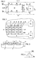
- Fig. 1 shows schematically the equivalent circuit diagram of the section of a monolithically integrated circuit within the dashed line 10, as is necessary to understand the invention.
- the pads 8 and 9 are attached, via which the power supply with the current Id of the integrated generator circuit Gi takes place.
- at least the "integrated generator circuit” is Power output stage of a self-oscillating generator circuit or controlled from outside the monolithically integrated circuit or a clocked logic circuit.
- the AC voltage Uc2 lies between the two potentials Vdd and Vss on an outer filter capacitor C2.
- the integrated generator circuit Gi supplies the rest of the clocked part of the monolithically integrated circuit with clock pulses, which are tapped at at least one clock output Ck via conductor tracks.
- clock pulses which are tapped at at least one clock output Ck via conductor tracks.
- VLSI highly integrated circuits
- clock pulse currents are required, which become apparent as superimposed interference currents of the entire interference current Is at the power supply input of the generator circuit Gi, that is to say also in the circuit of the contact pads 8 and 9.
- the effect of this interference current Is must therefore be made as harmless as possible in the form of electromagnetic interference radiation.
- An external capacitor C2 or an integrated capacitor C1 can be used for this purpose.
- an external capacitor C2 is largely ineffective since the electromagnetic interference radiation is proportional to the area enclosed by the interference current Is, that is to say, in the absence of the integrated capacitor C1, from the sum of the two areas A1 and A2.
- a capacitor Cl which is as large as possible as close as possible to the supply connections 11 and 12 of the monolithically integrated generator circuit Gi in such a way that the area Al, ie that of the interference current Is circumscribed area is as small as possible.
- the equivalent circuit of the monolithically integrated capacitor contains the capacitance C1, the series resistor R3 and the equivalent inductance L3. If an oscillator lying outside the integrated circuit is activated, a clock input Ck 'can be provided, which is located at a special contact spot.
- the equivalent circuit diagram of FIG. 1 also contains the integrated protective resistors R1 and R2, and the equivalent inductors L1 and L2, which contain the inductances of the leads to the outer capacitor, including those of the bonding wires to the outer connections 14 and 15.
- an integrated capacitor Cl which has the lowest possible series resistance R3 and a large specific capacitance , ie has the largest possible capacity per unit area in order to form an interference-reducing condensate on the smallest possible area.
- Such a capacitor is not shown to scale in principle in FIG. 2 as a detail and FIG. 3 in a cross-sectional view along the section line A-A 'of FIG. 2.
- the sectional view of FIG. 2 reveals the similarity to an Si gate transistor, namely electrodes applied to the gate insulator layers 1: tires 31 and 32, which in the Si gate process used in the production act as a diffusion mask for the production of the zone ( n) 5 can be used.
- a relatively thick field oxide layer 13 is produced outside the area circumscribed by the SDG line, which was produced, for example, using an oxidation masking layer.
- the extremely elongated electrode strips 31, 32 and others are produced by covering the exposed surface of the arrangement with a polycrystalline doped silicon layer and using a photolithographic etching process Electrode strips are etched out.
- the edge length ratio of the longitudinal extension of the strip to the edge length of the transverse extension of the strip should be at least 100: _ 1.
- the edge length ratio essentially determines the series resistance R3 and thus the quality of the capacitor.
- the quality of the capacitor is given by 1 / w.Cl. R3, a value that should be as large as possible.
- the limit of the achievable quality results from the accuracy of the photolithographic etching processes used.
- the sheet resistances of the contacting zone (s) 5, the electrode material and the contacting layers 4, 6 also have a further influence on the quality.
- FIG. 4 The equivalent circuit diagram of such an MIS capacitance is shown in FIG. 4 and shows an MIS field effect transistor, the source zone of which is short-circuited to the drain zone.
- This short circuit can be achieved both by means of the second contacting layer 6 and also according to FIG. 2 in that a distance remains on the end face of the electrode strips 31 and 32 and the edge of the field oxide layer 13, so that the electrode strips during the source-drain diffusion are surrounded by the contacting zones 12, which unite to form a common one.
- the contacting layers 4 and 6 are preferably comb-shaped and interlocking, as shown in FIG. 2.
- MIS capacitors with a relatively small area requirement which have 100 to 200 pF, can be implemented without further notice.
- each of the electrode strips must be contacted evenly and with low resistance over its surface. This can be done either over the entire surface of the electrode strip evenly by means of a first contacting layer, which contacts the electrode strip with low resistance except for one edge strip, or also by means of a contacting layer 4, which covers the electrode strip (s) 31 and 32 several times over uniformly over the surface area of the electrode strip or the electrode strips 31 and 32, which make contact with each of the electrode strips 31 and 32 through a contact opening of an insulator layer 7.
- the same procedure can be used for the contacting zones 5 in that the second contacting layer 6 contacts the contacting zone (s) 5 several times via contacts distributed evenly over the surface area of the contacting zone (s) 5 within a contacting opening 73 and 74 of an insulator layer 7 .
- the contacting layers 4 and 5 should naturally consist of a material whose specific resistance is lower than that of the silicon of the electrode strips, that is to say of a metal or also of a metal silicide.
- the power supply connections 11 and 12 were connected directly to the integrated MIS condensate br, in accordance with the points of view set out in connection with FIGS. 1 and 2, so that the radiating surface enclosed by the interference current Is became very small. It was possible to achieve that the ohmic series resistor R3 smaller than the capacitive resistor 1 / wC1 and the inductive series resistor wL3 also remained up to approximately 500 MHz smaller than the capacitive resistor 1 / wCl up to approximately 500 MHz. In the course of the contacting layers 6 and 4 shown in dashed lines in FIG. 2, the protective resistors R1 and R2 were inserted in series with the supply lines for better protection of the integrated MIS capacitor.
Landscapes
- Semiconductor Integrated Circuits (AREA)
Priority Applications (2)
| Application Number | Priority Date | Filing Date | Title |
|---|---|---|---|
| EP84109599A EP0171445A1 (fr) | 1984-08-11 | 1984-08-11 | Circuit intégré monolithique comprenant un condensateur de type MIS intégré |
| JP60174409A JPS6148958A (ja) | 1984-08-11 | 1985-08-09 | 金属‐絶縁物‐半導体集積キヤパシタ |
Applications Claiming Priority (1)
| Application Number | Priority Date | Filing Date | Title |
|---|---|---|---|
| EP84109599A EP0171445A1 (fr) | 1984-08-11 | 1984-08-11 | Circuit intégré monolithique comprenant un condensateur de type MIS intégré |
Publications (1)
| Publication Number | Publication Date |
|---|---|
| EP0171445A1 true EP0171445A1 (fr) | 1986-02-19 |
Family
ID=8192108
Family Applications (1)
| Application Number | Title | Priority Date | Filing Date |
|---|---|---|---|
| EP84109599A Withdrawn EP0171445A1 (fr) | 1984-08-11 | 1984-08-11 | Circuit intégré monolithique comprenant un condensateur de type MIS intégré |
Country Status (2)
| Country | Link |
|---|---|
| EP (1) | EP0171445A1 (fr) |
| JP (1) | JPS6148958A (fr) |
Cited By (5)
| Publication number | Priority date | Publication date | Assignee | Title |
|---|---|---|---|---|
| DE3915594A1 (de) * | 1988-05-16 | 1989-11-30 | Hitachi Ltd | Halbleitervorrichtung |
| EP0377502A1 (fr) * | 1989-01-06 | 1990-07-11 | AT&T GLOBAL INFORMATION SOLUTIONS INTERNATIONAL INC. | Condensateur pour circuit intégré |
| EP0817249A3 (fr) * | 1996-06-27 | 1999-01-20 | Nec Corporation | Méthode de conception d'une capacité d'un transistor MOS |
| ES2229947A1 (es) * | 2003-10-14 | 2005-04-16 | Universitat Politecnica De Catalunya | Estructura de alta capacidad y baja resistencia serie equivalente en tecnologia integrada cmos estandar. |
| EP3640984A1 (fr) * | 2018-10-19 | 2020-04-22 | MediaTek Singapore Pte Ltd. | Dispositif de circuit intégré |
Citations (3)
| Publication number | Priority date | Publication date | Assignee | Title |
|---|---|---|---|---|
| DE1940300A1 (de) * | 1968-08-21 | 1970-08-06 | Rca Corp | Halbleiterkondensator |
| FR2024788A1 (fr) * | 1968-10-10 | 1970-09-04 | Gen Electric | |
| FR2124353A1 (fr) * | 1971-02-08 | 1972-09-22 | Trw Inc |
-
1984
- 1984-08-11 EP EP84109599A patent/EP0171445A1/fr not_active Withdrawn
-
1985
- 1985-08-09 JP JP60174409A patent/JPS6148958A/ja active Pending
Patent Citations (3)
| Publication number | Priority date | Publication date | Assignee | Title |
|---|---|---|---|---|
| DE1940300A1 (de) * | 1968-08-21 | 1970-08-06 | Rca Corp | Halbleiterkondensator |
| FR2024788A1 (fr) * | 1968-10-10 | 1970-09-04 | Gen Electric | |
| FR2124353A1 (fr) * | 1971-02-08 | 1972-09-22 | Trw Inc |
Non-Patent Citations (2)
| Title |
|---|
| ELEKTRONIK, Heft 5, 1973, München; L. TALAMONTI "Binäre Kapazitäten in MOS-Schaltungen", Seiten 179-181 * |
| PATENT ABSTRACTS OF JAPAN, Band 8, Nr. 149, 12. Juli 1984, Seite (E-255) (1586); & JP-A-59-54248 (FUJITSU K.K.) 29-03-1984 * |
Cited By (6)
| Publication number | Priority date | Publication date | Assignee | Title |
|---|---|---|---|---|
| DE3915594A1 (de) * | 1988-05-16 | 1989-11-30 | Hitachi Ltd | Halbleitervorrichtung |
| EP0377502A1 (fr) * | 1989-01-06 | 1990-07-11 | AT&T GLOBAL INFORMATION SOLUTIONS INTERNATIONAL INC. | Condensateur pour circuit intégré |
| EP0817249A3 (fr) * | 1996-06-27 | 1999-01-20 | Nec Corporation | Méthode de conception d'une capacité d'un transistor MOS |
| US5966518A (en) * | 1996-06-27 | 1999-10-12 | Nec Corporation | Capacitor designing method of MOS transistor |
| ES2229947A1 (es) * | 2003-10-14 | 2005-04-16 | Universitat Politecnica De Catalunya | Estructura de alta capacidad y baja resistencia serie equivalente en tecnologia integrada cmos estandar. |
| EP3640984A1 (fr) * | 2018-10-19 | 2020-04-22 | MediaTek Singapore Pte Ltd. | Dispositif de circuit intégré |
Also Published As
| Publication number | Publication date |
|---|---|
| JPS6148958A (ja) | 1986-03-10 |
Similar Documents
| Publication | Publication Date | Title |
|---|---|---|
| DE69224709T2 (de) | Halbleiteranordnung mit verbesserter Durchbruchspannungs-Charakteristik | |
| DE4013643C2 (de) | Bipolartransistor mit isolierter Steuerelektrode und Verfahren zu seiner Herstellung | |
| DE69331793T2 (de) | Integriertes Leistungshalbleiterschaltkreisbauelement mit gleichförmiger elektrischer Feldverteilung | |
| DE3118674A1 (de) | Duennfilm-transistor | |
| DE2559360A1 (de) | Halbleiterbauteil mit integrierten schaltkreisen | |
| DE1639255C2 (de) | Integrierte Halbleiterschaltung mit einem Isolierschicht-Feldeffekttransistor | |
| DE2903534A1 (de) | Feldeffekttransistor | |
| EP0059878A1 (fr) | Source de tension de référence intégrée monolithique | |
| DE69417199T2 (de) | LC-Element, Halbleiteranordnung, und Verfahren zur Herstellung des LC-Elements | |
| DE69423568T2 (de) | LC-Element, Halbleiteranordnung und Verfahren zur Herstellung des LC-Elements | |
| DE2262943A1 (de) | Verfahren zur verhinderung einer unerwuenschten inversion | |
| DE69430091T2 (de) | Halbleiterbauelement mit LC-Element und Verfahren zur Herstellung | |
| DE3844393A1 (de) | Schaltungsanordnung mit geschalteter spule | |
| DE69024234T2 (de) | Kondensator für eine integrierte Schaltung | |
| DE1514017A1 (de) | Halbleiteranordnung | |
| DE69329543T2 (de) | Herstellung eines Feldeffekttransistors mit integrierter Schottky-Klammerungsdiode | |
| EP0282617A1 (fr) | Circuit intégré comprenant un support électroconducteur | |
| DE1464395A1 (de) | Feldeffekt-Transistor | |
| EP0341453B1 (fr) | Elément semi-conducteur MOS à haute tension de blocage | |
| DE2844878A1 (de) | Integrierbarer isolierschicht-feldeffekttransistor | |
| DE2629468A1 (de) | Temperaturkompensierter oszillator | |
| DE2236897B2 (fr) | ||
| DE1930606A1 (de) | Halbleiterbauelement mit einem Feldeffekttransistor mit isolierter Torelektrode und Schaltungsanordnung mit einem solchen Halbleiterbauelement | |
| DE1935862B2 (de) | Kettenverstaerker mit feld effekt transistoren | |
| DE1962403A1 (de) | Verzoegerungseinrichtung fuer elektrische Signale |
Legal Events
| Date | Code | Title | Description |
|---|---|---|---|
| PUAI | Public reference made under article 153(3) epc to a published international application that has entered the european phase |
Free format text: ORIGINAL CODE: 0009012 |
|
| 17P | Request for examination filed |
Effective date: 19850801 |
|
| AK | Designated contracting states |
Designated state(s): DE FR GB IT NL |
|
| 17Q | First examination report despatched |
Effective date: 19870406 |
|
| STAA | Information on the status of an ep patent application or granted ep patent |
Free format text: STATUS: THE APPLICATION HAS BEEN WITHDRAWN |
|
| 18W | Application withdrawn |
Withdrawal date: 19870715 |
|
| RIN1 | Information on inventor provided before grant (corrected) |
Inventor name: GOLLINGER, WOLFGANG Inventor name: BRUELL, JOCHEN |