EP0171718A2 - Circuit décodeur dans un chip de mémoire intégrée - Google Patents
Circuit décodeur dans un chip de mémoire intégrée Download PDFInfo
- Publication number
- EP0171718A2 EP0171718A2 EP85109709A EP85109709A EP0171718A2 EP 0171718 A2 EP0171718 A2 EP 0171718A2 EP 85109709 A EP85109709 A EP 85109709A EP 85109709 A EP85109709 A EP 85109709A EP 0171718 A2 EP0171718 A2 EP 0171718A2
- Authority
- EP
- European Patent Office
- Prior art keywords
- power supply
- decoder circuit
- supply voltage
- transistor
- gate
- Prior art date
- Legal status (The legal status is an assumption and is not a legal conclusion. Google has not performed a legal analysis and makes no representation as to the accuracy of the status listed.)
- Granted
Links
Images

Classifications
-
- G—PHYSICS
- G11—INFORMATION STORAGE
- G11C—STATIC STORES
- G11C16/00—Erasable programmable read-only memories
- G11C16/02—Erasable programmable read-only memories electrically programmable
- G11C16/06—Auxiliary circuits, e.g. for writing into memory
- G11C16/10—Programming or data input circuits
- G11C16/12—Programming voltage switching circuits
-
- G—PHYSICS
- G11—INFORMATION STORAGE
- G11C—STATIC STORES
- G11C16/00—Erasable programmable read-only memories
- G11C16/02—Erasable programmable read-only memories electrically programmable
- G11C16/06—Auxiliary circuits, e.g. for writing into memory
- G11C16/08—Address circuits; Decoders; Word-line control circuits
-
- G—PHYSICS
- G11—INFORMATION STORAGE
- G11C—STATIC STORES
- G11C8/00—Arrangements for selecting an address in a digital store
- G11C8/10—Decoders
Definitions
- the present invention relates to a decoder circuit used in an integrated semiconductor circuit (IC) memory chip or die which comprises a memory cell matrix consisting of a plurality of memory cells. More particularly, the present invention relates to a decoder circuit adapted for respective memory cell which requires two kinds of power supply voltages for programming or reading the data into or from the memory cell.
- IC integrated semiconductor circuit
- EPROM erasable programmable read only memory
- the memory cell matrix is composed of a plurality of word-lines and bit-lines, and an EPROM cell is placed at each intersection point of respective word-line and bit--line.
- the EPROM cell requires two kinds of power supply voltages - a high power supply voltage and a low power supply voltage -, for programming and reading out the data into and from the cell respectively; the high and the low power supply voltages are supplied to the IC memory chip from its exterior.
- a designated EPROM cell transistor is selected by external address signals given from a computer system to which the IC memory chip belongs; the selection is done by applying row and column address signals to the row and the column decoder circuits respectively. For example, when the row address signals are applied to the row decoder circuits, one of the row decoder circuits outputs an H level. As a result, only one word-line is raised up to the H level so that the EPROM cell transistors, of which gates are connected to the word-line, are ready to read out the data. The same process is also enforced to the bit-line through the column decoder circuit, so that a designated EPROM cell transistor can be selected so as to be ready to read out the data. In this case, it is said that the row and column decoder circuits are in a selective state and other decoder circuits are in a non-selective state hereinafter.
- total number of the decoder circuits fabricated in the IC memory chip are as many as the total number of the word-lines and the bit-lines.
- the row decoder circuit and the column decoder circuit are similar to each other, so the row decoder circuit will be discussed of hereinafter.
- Fig. 2 is a conventional row decoder circuit of the prior art, and it shows a case that the row decoder circuit receives a unique combination of address signals composed of 3 bits, a 0 /a 0 ⁇ a 2 /a 2 : a i /a i means a. or a i , and a. means an inverted signal of a i such that when a i is a signal having a high level, i is a signal having a low level.
- These internal address signals are generated inside the semiconductor chip in response to the external address signals applied to the chip from the exterior. So, the row decoder circuit of Fig. 2 is one of eight row decoder circuits, and a word-line WL is one of eight word-lines.
- V cc is a fixed low power supply voltage (5 volts (V) for example) and V ppi is a variable power supply voltage.
- the variable power supply voltage V ppi is changed so as to be a high power supply voltage V pp (12.5 V or 21 V for example) when a datum is programmed into an EPROM, and the low power supply voltage V cc when a datum is read out from an EPROM.
- V ss means the earth potential.
- Transistors Q n1 ⁇ Q n3 and Q p1 compose a NAND gate and receives 3 address inputs at the same time.
- the output level of the NAND gate at output node X becomes low (L) when all of the 3 address inputs are in a high (H) level; this is said that the decoder circuit is in the selective state.
- the output level becomes H when at least one of the 3 address inputs is in the L level; this is said that the decoder circuit is in the non-selective state.
- the output of the NAND gate at node X is fed to the gates of transistors Qp 3 and Q n5 , those of which compose a CMO S invertor, through a transfer gate Q n4 .
- the CMOS inverter- operates as follows: when the output level of the NAND gate at node X becomes L, transistors Q n5 and Q p3 become OFF and ON-respectively so that an H level (equal to the level of V ppi ) is outputted to word-line WL, and when the level at node X becomes H, transistors Q n5 and Qp 3 become ON and OFF respectively so that an L level is outputted to word-line WL.
- the level on word-line WL becomes H so that an EPROM cell transistor of which gates are connected to the word--line becomes able to read out the datum or program the datum.
- Transistor Q p2 is a pull-up transistor used as a level compensator.
- V ppi is switched to high power supply voltage V pp .
- an input signal (level) of invertor Qp3 - Q n5 could not be raised up enough to high voltage; it would be limited as low as power supply voltage V . This is due to a fact that the NAND gate always uses low power supply voltage V cc as the power supply voltage.
- the invertor Qp 3 - Q n5 would become unstable; the invertor could not produce a stable L level.
- a large DC current would flow constantly through transistors Q p3 and Q n5 from the power supply to the earth since both the transistors would be on under this condition, resulting in large power consumption.
- transistor Q p2 when the level on the word-line WL becomes L, the level L is fed back to transistor Qp 2 making it ON, so high power supply voltage V pp is applied to the gates of the invertor Q p3 - Q n5 so that transistor Q p3 completely cuts off; then the level on the word-line WL can be fixed to L so that word-line WL completely becomes a non-selected state.
- the level at node X and the level at the gates of the invertor Q p3 - Q n5 become almost equal to low power supply voltage V cc and high power supply voltage V pp respectively.
- the transfer gate of transistor Q n4 is to prevent the competition of the V cc and V pp ; when transistor Qp 2 pulls up the voltage on the gates of the invertor Q p3 - Q n5 to high power supply voltage V pp , transistor Q n4 is driven to be cut off.
- variable power supply voltage V ppi becomes low power supply voltage V and the compensator and the transfer gate functions similarly to the above in the programming mode.
- the transistors of the compensator and the transfer gate are necessary for maintaining each level of the word-line and the bit-line so as to avoid a large constant current at the CMOS invertor and obtain a stable low level output in respective row and column decoder circuit.
- the transistors of the compensator and the transfer gate are necessary for maintaining each level of the word-line and the bit-line so as to avoid a large constant current at the CMOS invertor and obtain a stable low level output in respective row and column decoder circuit.
- there are many IC elements like transistors and wirings in each decoder circuits and a plenty of the decoder circuits as many as the same number of the row and bit lines are necessary in the IC memory chip. So, even though the memory matrix consisting of the EPROMs can be integrated in a high packing density with the skill of the art, the area for the decoder circuits becomes dominant in a space factor and brings difficulty of fabricating a small IC memory chip. Especially, the area becomes a big problem for designing compactly
- An object of the present invention is to reduce the IC elements of the decoder circuit which is fabricated with respective word-line and bit-line of a memory matrix in an IC memory chip.
- Another object of the present invention is to simplify the power supply voltage applied to the decoder circuits so that only a kind of power supply voltage is enough to operate the decoder circuits.
- Still another object of the present invention is to reduce the DC current spent in the decoder circuits.
- More another object of the present invention is to reduce the fabricating cost of the decoder circuits.
- a further object of the present invention is to realize a high packing density of the IC memory chip, to decrease the DC current spent in the IC memory chip, and to reduce the fabricating cost of the IC memory chip.
- the above objects of the present invention are achieved by simplifying the ordinary decoder circuit so as to be composed of only a decoding logic gate, particularly a NAND gate and a CMOS invertor by removing a compensator and a transfer gate from the ordinary decoder circuit.
- the simplification is made by applying a depletion type transistor to the load of the NAND gate and making the depletion type transistor operate as a constant current load. By doing so, the same variable power supply voltage can be applied to the NAND gate and the invertor, so that the NAND gate output can directly drive the invertor.
- the compensator, a lead which has been necessary to feed the output of the invertor back to the compensator, and the transfer gate are no necessary any more to the decoder circuit.
- Fig. 1 is a circuit diagram of a decoder circuit embodying the present invention.
- the same reference symbol to that in Fig. 2 designates the same part to that in Fig. 2.
- the different points of Fig. 1 from Fig. 2 are as follows: firstly, replacing transistor Qp l , which has been the E type p channel MOS transistor used as a load of the NAND gate in the ordinary decoder circuit in Fig.
- transistor Q nd is a D type n channel MIS transistor and its gate and source are connected in common, the internal resistance of transistor Q nd changes so as to become large when the applied variable power supply voltage V . becomes high power supply voltage V pp and to become small when applied variable power supply voltage V ppi becomes low power supply voltage V cc .
- transistor Q nd functions as a constant current load.
- the decoder circuit When all of address signal inputs are at H level, the output of the NAND gate at node X becomes an L level; the decoder circuit becomes the selective state. In this case, either the decoder circuit operates under the programming mode or the reading mode, the output L level is always driven to earth potential V ss and directly fed to the gates of the invertor Qp 3 - Q n5 : transistor Q nd is the depletion type and makes flow the constant current as mentioned above, so the output L level can be driven to earth potential V ss by designing the ratio of the conductance between the NAND gate load (transistor Q nd ) and the NAND gate elements (transistors Q n1' Q n2' and Q n3 ). Therefore, invertor Qp 3 - Q n5 can stably produce an H level on the word-line WL.
- the output of the NAND gate at node X becomes an H level; the decoder circuit becomes the non-selective state.
- V ppi becomes V pp or V cc respectively; then the output H level becomes V pp or V cc and directly drives invertor Qp 3 - Q nS .
- transistor Qp 3 completely cuts off and no constant DC current flows through the invertor. Therefore, the problem of large power consumption can be avoided and the invertor can stably produce an L level on word-line WL.
- the output CMOS invertor also provides a sufficiently large driving capability.
- the decoder circuit of Fig. 1 stably operates without the compensator, the associated feed back lead, and the transfer gate.
- the removement of such elements brings a great effect for realizing the high packing density of the IC memory chip, especially of the chip having a large memory capacitor like 256 K-bit or 512 K-bit.
- a size of the decoder circuit decides a pitch of the word-lines or the bit-lines, in other word, the pitch is a large factor to decide the size of the IC memory chip. Therefore, realizing the high packing density of the decoder circuit is very effective for increasing that of the IC memory chip.
- a United States Patent No. 4,374,430 is a patent which relates to also the decoder circuit used in an IC memory chip comprising the EPROMs.
- the patent pays attention to the reduction of the DC current, which is spent in the IC memory chip, rather than increasing the packing density.
- the present invention is for realizing the high packing density, which is also effective to reduce the DC current.
- high power supply voltage V pp and low power supply voltage V cc are supplied from the exterior of the IC memory chip.
- the IC memory chip is set into a "programmer” and high power supply voltage V pp is applied to the IC memory from its exterior, and after that, the IC memory chip is mounted in a printing board and low power supply voltage V cc is applied from the exterior, the printed board, in the reading mode. Therefore, the shape, the size, and the number and the positions of the terminals of the IC memory chip are desired to meet with a technical standard such as the standard of the Joint Electron Device Engineering Council (JEDEC).
- JEDEC Joint Electron Device Engineering Council
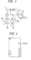
- Fig. 4 is an example of the terminal positions of the IC memory chip: the figure only shows typical terminals relating to the following explanation.
- Symbol OE is an output enable terminal to which a control signal of a TTL (transistor transistor logic) level comes in when the chip is in the reading mode; when the control signal is an H level, output terminals O1 ⁇ 08 become invalid (floating state) respectively, and when the control signal is an L level, the terminals become valid.
- 21 V or 12.5 V is applied to the V pp terminal.
- terminal OE if terminal OE is used for both, the OE signal and high power supply voltage V pp , terminal V pp can be used for another signal, an address signal for example.
- the IC memory chip has to provide an OE/V pp switching circuit.
- Fig. 3 shows an example of the OE/V pp switching circuit.
- reference symbols T 1 , T 3 , T 4 , and T 6 are the E type p channel MOS transistors
- T 5 and T 7 are the E type n channel MOS transistors
- T 2 is a D type n channel MOS transistor whose threshold voltage is set to a proper voltage from a range of 0 V ⁇ low power supply voltage V cc .
- Transistors T 4 and T 5 compose a CMOS invertor I
- transistors T 6 and T 7 compose a CMOS invertor I 2 .
- Transistor T 3 operates as a level shifter so that it becomes ON only when its power supply voltage becomes more than 10 V.
- Transistor T 3 and invertors I I and I 2 compose a voltage detecting circuit 2
- transistors T 1 and T 2 compose a voltage selecting circuit 3.
- output enable signal OE which is in the TTL level being always less than 10 V, is applied to a terminal 1. So, transistor T 3 becomes OFF, so that the output R of invertor I 2 becomes an H level which is equal to low power supply voltage V cc . Then only transistor T 2 of the voltage selecting circuit 3 becomes ON. Therefore, an output voltage V X of the OE/V pp switching circuit produces low power supply voltage V cc .
- high power supply voltage V pp is applied to terminal 1.
- the high power supply voltage V pp is more than 10 V
- transistor T 3 becomes ON, so that output R falls down to an L level.
- transistors T 1 and T 2 become ON and OFF respectively, so that output V X becomes high power supply voltage V pp .
- terminal V pp in Fig. 4 can be used to another signal, which means one terminal can be reduced from the IC memory device.
Landscapes
- Engineering & Computer Science (AREA)
- Microelectronics & Electronic Packaging (AREA)
- Read Only Memory (AREA)
Applications Claiming Priority (4)
| Application Number | Priority Date | Filing Date | Title |
|---|---|---|---|
| JP166114/84 | 1984-08-08 | ||
| JP59166114A JPS6145496A (ja) | 1984-08-08 | 1984-08-08 | デコ−ダ回路 |
| JP59182417A JPS6161295A (ja) | 1984-08-31 | 1984-08-31 | 半導体記憶装置 |
| JP182417/84 | 1984-08-31 |
Publications (3)
| Publication Number | Publication Date |
|---|---|
| EP0171718A2 true EP0171718A2 (fr) | 1986-02-19 |
| EP0171718A3 EP0171718A3 (en) | 1987-12-02 |
| EP0171718B1 EP0171718B1 (fr) | 1992-03-11 |
Family
ID=26490607
Family Applications (1)
| Application Number | Title | Priority Date | Filing Date |
|---|---|---|---|
| EP85109709A Expired - Lifetime EP0171718B1 (fr) | 1984-08-08 | 1985-08-02 | Circuit décodeur dans un chip de mémoire intégrée |
Country Status (4)
| Country | Link |
|---|---|
| US (1) | US4782247A (fr) |
| EP (1) | EP0171718B1 (fr) |
| KR (1) | KR900002910B1 (fr) |
| DE (1) | DE3585573D1 (fr) |
Cited By (7)
| Publication number | Priority date | Publication date | Assignee | Title |
|---|---|---|---|---|
| FR2634576A1 (fr) * | 1988-07-21 | 1990-01-26 | Intel Corp | Etage de pilotage de lecture et de programmation pour composant a reseau logique programmable |
| EP0366403A3 (fr) * | 1988-10-25 | 1991-04-24 | Fujitsu Limited | Dispositif de mémoire à semi-conducteur |
| EP0346671A3 (fr) * | 1988-06-17 | 1991-05-29 | Motorola, Inc. | Programmation d'un EPROM |
| EP0376065A3 (fr) * | 1988-12-24 | 1991-07-24 | Kabushiki Kaisha Toshiba | Circuit intégré de mémoire à semi-conducteurs |
| EP0406007A3 (en) * | 1989-06-30 | 1992-09-30 | Fujitsu Limited | Non volatile semiconductor memory device |
| EP0443777A3 (en) * | 1990-02-19 | 1992-11-04 | Fujitsu Limited | Write circuit for non-volatile memory device |
| US5412331A (en) * | 1992-10-31 | 1995-05-02 | Samsung Electronics Co., Ltd. | Word line driving circuit of a semiconductor memory device |
Families Citing this family (14)
| Publication number | Priority date | Publication date | Assignee | Title |
|---|---|---|---|---|
| US5142494A (en) * | 1990-02-26 | 1992-08-25 | Eastman Kodak Company | Memory based line-delay architecture |
| US5058065A (en) * | 1990-02-26 | 1991-10-15 | Eastman Kodak Company | Memory based line-delay architecture |
| GB9007790D0 (en) | 1990-04-06 | 1990-06-06 | Lines Valerie L | Dynamic memory wordline driver scheme |
| JPH04225182A (ja) | 1990-12-26 | 1992-08-14 | Toshiba Corp | 半導体記憶装置 |
| US5506803A (en) * | 1992-04-01 | 1996-04-09 | Intel Corporation | Apparatus and method for minimizing verify time in a semiconductor memory by constantly charging n-well capacitance |
| US5675824A (en) * | 1992-09-30 | 1997-10-07 | Intel Corporation | Programmable logic having selectable output voltages |
| JP3267436B2 (ja) * | 1993-04-19 | 2002-03-18 | 三菱電機株式会社 | 半導体装置 |
| US5696464A (en) * | 1993-10-22 | 1997-12-09 | At&T Global Information Solutions Company | Output driver adaptable to power supply variation |
| KR0124046B1 (ko) * | 1993-11-18 | 1997-11-25 | 김광호 | 반도체메모리장치의 승압레벨 감지회로 |
| US5798885A (en) * | 1994-06-06 | 1998-08-25 | Fujitsu Limited | Head positioning control for disk apparatus using peak detection, polarity detection and sector mark detection |
| US5796673A (en) | 1994-10-06 | 1998-08-18 | Mosaid Technologies Incorporated | Delay locked loop implementation in a synchronous dynamic random access memory |
| US8782477B2 (en) * | 2011-05-11 | 2014-07-15 | Jabil Circuit, Inc. | High-speed serial interface bridge adapter for signal integrity verification |
| US8913436B2 (en) * | 2013-03-14 | 2014-12-16 | Freescale Semiconductor, Inc. | Non-volatile memory (NVM) with word line driver/decoder using a charge pump voltage |
| WO2023037370A1 (fr) | 2021-09-13 | 2023-03-16 | Neologic Ltd | Mise en œuvre de portes logiques tolérantes aux fuites |
Family Cites Families (9)
| Publication number | Priority date | Publication date | Assignee | Title |
|---|---|---|---|---|
| GB1375958A (en) * | 1972-06-29 | 1974-12-04 | Ibm | Pulse circuit |
| US3982138A (en) * | 1974-10-09 | 1976-09-21 | Rockwell International Corporation | High speed-low cost, clock controlled CMOS logic implementation |
| JPS5833638B2 (ja) * | 1979-09-21 | 1983-07-21 | 株式会社日立製作所 | メモリ装置 |
| JPS5673542A (en) * | 1979-11-22 | 1981-06-18 | Kureha Chem Ind Co Ltd | Adsorbent |
| JPS5831677B2 (ja) * | 1979-11-26 | 1983-07-07 | 富士通株式会社 | 半導体記億装置 |
| GB2094086B (en) * | 1981-03-03 | 1985-08-14 | Tokyo Shibaura Electric Co | Non-volatile semiconductor memory system |
| JPS57147196A (en) * | 1981-03-06 | 1982-09-10 | Fujitsu Ltd | Read-only memory |
| US4415993A (en) * | 1981-11-23 | 1983-11-15 | The United States Of America As Represented By The Secretary Of The Air Force | Fast access non-volatile memory |
| US4514829A (en) * | 1982-12-30 | 1985-04-30 | International Business Machines Corporation | Word line decoder and driver circuits for high density semiconductor memory |
-
1985
- 1985-07-29 US US06/759,980 patent/US4782247A/en not_active Expired - Fee Related
- 1985-08-02 DE DE8585109709T patent/DE3585573D1/de not_active Expired - Lifetime
- 1985-08-02 EP EP85109709A patent/EP0171718B1/fr not_active Expired - Lifetime
- 1985-08-02 KR KR1019850005581A patent/KR900002910B1/ko not_active Expired
Cited By (10)
| Publication number | Priority date | Publication date | Assignee | Title |
|---|---|---|---|---|
| EP0346671A3 (fr) * | 1988-06-17 | 1991-05-29 | Motorola, Inc. | Programmation d'un EPROM |
| FR2634576A1 (fr) * | 1988-07-21 | 1990-01-26 | Intel Corp | Etage de pilotage de lecture et de programmation pour composant a reseau logique programmable |
| EP0366403A3 (fr) * | 1988-10-25 | 1991-04-24 | Fujitsu Limited | Dispositif de mémoire à semi-conducteur |
| EP0376065A3 (fr) * | 1988-12-24 | 1991-07-24 | Kabushiki Kaisha Toshiba | Circuit intégré de mémoire à semi-conducteurs |
| US5065361A (en) * | 1988-12-24 | 1991-11-12 | Kabushiki Kaisha Toshiba | Semiconductor memory integrated circuit |
| EP0406007A3 (en) * | 1989-06-30 | 1992-09-30 | Fujitsu Limited | Non volatile semiconductor memory device |
| US5463583A (en) * | 1989-06-30 | 1995-10-31 | Fujitsu Limited | Non-volatile semiconductor memory device |
| EP0443777A3 (en) * | 1990-02-19 | 1992-11-04 | Fujitsu Limited | Write circuit for non-volatile memory device |
| US5293344A (en) * | 1990-02-19 | 1994-03-08 | Fujitsu Limited | Write circuit for non-volatile memory device |
| US5412331A (en) * | 1992-10-31 | 1995-05-02 | Samsung Electronics Co., Ltd. | Word line driving circuit of a semiconductor memory device |
Also Published As
| Publication number | Publication date |
|---|---|
| KR860002150A (ko) | 1986-03-26 |
| DE3585573D1 (de) | 1992-04-16 |
| EP0171718A3 (en) | 1987-12-02 |
| US4782247A (en) | 1988-11-01 |
| KR900002910B1 (ko) | 1990-05-03 |
| EP0171718B1 (fr) | 1992-03-11 |
Similar Documents
| Publication | Publication Date | Title |
|---|---|---|
| EP0171718A2 (fr) | Circuit décodeur dans un chip de mémoire intégrée | |
| US6535430B2 (en) | Wordline decoder for flash memory | |
| EP0199305B1 (fr) | Mémoire morte programmable utilisant une source d'alimentation de programmation réduite | |
| US4103189A (en) | Mos buffer circuit | |
| US7957176B2 (en) | Semiconductor memory device with improved resistance to disturbance and improved writing characteristic | |
| US5594687A (en) | Completely complementary MOS memory cell with tunneling through the NMOS and PMOS transistors during program and erase | |
| US5039882A (en) | Address decoder circuit for non-volatile memory | |
| US6477091B2 (en) | Method, apparatus, and system to enhance negative voltage switching | |
| US5274597A (en) | Semiconductor memory device capable of driving divided word lines at high speed | |
| US6650567B1 (en) | Nonvolatile semiconductor memories with a NAND logic cell structure | |
| US7474553B2 (en) | Device writing to a plurality of rows in a memory matrix simultaneously | |
| EP0370308A2 (fr) | Dispositif de mémoire semi-conducteur non volatile, ayant à l'étage d'entrée d'un décodeur d'adresses, un décaleur de niveau pour générer une tension de programmation | |
| EP1581952B1 (fr) | Reseau de cellules memoires a polarisation de source | |
| US5513147A (en) | Row driving circuit for memory devices | |
| US6097636A (en) | Word line and source line driver circuitries | |
| KR100744103B1 (ko) | 플래쉬메모리장치의로우디코더 | |
| GB2308699A (en) | Method for driving word lines in semicnductor memory device | |
| US5400285A (en) | Semiconductor integrated circuit device | |
| US4901281A (en) | Semiconductor memory device having two column transfer gate transistor groups independently provided for a sense amplifier and a programmed circuit | |
| US6661734B2 (en) | Semiconductor memory device | |
| US20040141394A1 (en) | Memory circuit apparatus | |
| US4924438A (en) | Non-volatile semiconductor memory including a high voltage switching circuit | |
| KR950000029B1 (ko) | 기생용량에 의해 야기된 오동작을 방지하기 위한 eprom의 디코더 회로 | |
| US4198700A (en) | Column decode circuit for random access memory | |
| EP0136229A2 (fr) | Amplificateur de lecture |
Legal Events
| Date | Code | Title | Description |
|---|---|---|---|
| PUAI | Public reference made under article 153(3) epc to a published international application that has entered the european phase |
Free format text: ORIGINAL CODE: 0009012 |
|
| AK | Designated contracting states |
Designated state(s): DE FR GB |
|
| PUAL | Search report despatched |
Free format text: ORIGINAL CODE: 0009013 |
|
| AK | Designated contracting states |
Kind code of ref document: A3 Designated state(s): DE FR GB |
|
| 17P | Request for examination filed |
Effective date: 19880113 |
|
| 17Q | First examination report despatched |
Effective date: 19890614 |
|
| GRAA | (expected) grant |
Free format text: ORIGINAL CODE: 0009210 |
|
| AK | Designated contracting states |
Kind code of ref document: B1 Designated state(s): DE FR GB |
|
| REF | Corresponds to: |
Ref document number: 3585573 Country of ref document: DE Date of ref document: 19920416 |
|
| ET | Fr: translation filed | ||
| PLBE | No opposition filed within time limit |
Free format text: ORIGINAL CODE: 0009261 |
|
| STAA | Information on the status of an ep patent application or granted ep patent |
Free format text: STATUS: NO OPPOSITION FILED WITHIN TIME LIMIT |
|
| 26N | No opposition filed | ||
| PGFP | Annual fee paid to national office [announced via postgrant information from national office to epo] |
Ref country code: GB Payment date: 19970724 Year of fee payment: 13 |
|
| PGFP | Annual fee paid to national office [announced via postgrant information from national office to epo] |
Ref country code: FR Payment date: 19970811 Year of fee payment: 13 Ref country code: DE Payment date: 19970811 Year of fee payment: 13 |
|
| PG25 | Lapsed in a contracting state [announced via postgrant information from national office to epo] |
Ref country code: GB Free format text: LAPSE BECAUSE OF NON-PAYMENT OF DUE FEES Effective date: 19980802 |
|
| GBPC | Gb: european patent ceased through non-payment of renewal fee |
Effective date: 19980802 |
|
| PG25 | Lapsed in a contracting state [announced via postgrant information from national office to epo] |
Ref country code: FR Free format text: LAPSE BECAUSE OF NON-PAYMENT OF DUE FEES Effective date: 19990430 |
|
| PG25 | Lapsed in a contracting state [announced via postgrant information from national office to epo] |
Ref country code: DE Free format text: LAPSE BECAUSE OF NON-PAYMENT OF DUE FEES Effective date: 19990601 |
|
| REG | Reference to a national code |
Ref country code: FR Ref legal event code: ST |