EP0172912A1 - Kontaktmaterial für vakuumabbrecher - Google Patents
Kontaktmaterial für vakuumabbrecher Download PDFInfo
- Publication number
- EP0172912A1 EP0172912A1 EP84903371A EP84903371A EP0172912A1 EP 0172912 A1 EP0172912 A1 EP 0172912A1 EP 84903371 A EP84903371 A EP 84903371A EP 84903371 A EP84903371 A EP 84903371A EP 0172912 A1 EP0172912 A1 EP 0172912A1
- Authority
- EP
- European Patent Office
- Prior art keywords
- amount
- components
- alloy
- contact material
- state
- Prior art date
- Legal status (The legal status is an assumption and is not a legal conclusion. Google has not performed a legal analysis and makes no representation as to the accuracy of the status listed.)
- Granted
Links
Images






Classifications
-
- H—ELECTRICITY
- H01—ELECTRIC ELEMENTS
- H01H—ELECTRIC SWITCHES; RELAYS; SELECTORS; EMERGENCY PROTECTIVE DEVICES
- H01H1/00—Contacts
- H01H1/02—Contacts characterised by the material thereof
- H01H1/0203—Contacts characterised by the material thereof specially adapted for vacuum switches
- H01H1/0206—Contacts characterised by the material thereof specially adapted for vacuum switches containing as major components Cu and Cr
Definitions
- the present invention relates to a contact material for vacuum interrupter which is spectacular in breakdown voltage and has a high interrupting ability.
- Vacuum interrupters are expanding its application range very rapidly because of no need of maintenance, no environmental pollution and spectacular interrupting ability, or the like. And accompanying the above, a larger interrupting capacity and higher breakdown voltage are being demanded. On the other hand, for ability of vacuum interrupter, there is a very great element which is determined by contact material in a vacuum container.
- the present invention constituted a contact material for vacuum interrupter by containing copper and chromium, and as other component(s) one component selected from a group consisting of silicon, titanium, zirconium and aluminum.
- FIG. 1 is a sectional view showing construction of a vacuum switching tube for applying one embodiment of the invention
- FIG. 2 is an enlarged sectional view of part of an electrode of FIG. 1
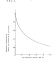
- FIG. 3 is a characteristic view showing change of breakdown voltage ability when Si addition amount is changed to an alloy which is a contact material of the present invention wherein Cr amount is fixed at 25 wt %
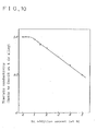
- FIG. 4 is a characteristic diagram showing change of electric conductivity when Si addition amount is changed to an alloy which is a contact material of the present invention wherein Cr amount is fixed at 25 wt %
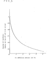
- FIG. 5 is a characteristic curve showing change of hardness when Si addition amount is changed to an alloy which is a contact material of the present invention wherein Cr amount is fixed at 25 wt %.
- FIG. 6 is a characteristic diagram showing change of interrupting capacity when Ti addition amount is changed to an alloy which is a contact material of the present invention wherein Cr amount is fixed at 25 wt %
- FIG. 7 is a characteristic diagram showing change of electric conductivity when Ti addition amount is changed to an alloy which is a contact material of the present invention wherein Cr amount is fixed at 25 wt %
- FIG. 8 is a characteristic curve showing changes of hardness (A) and breakdown voltage ability (B) when Ti addition amount is changed to an alloy which is a contact material of the present invention wherein Cr amount is fixed 25 wt %.
- FIG. 9 is a characteristic view showing change of interrupting capacity when Zr addition amount is changed to an alloy which is a contact material of the present invention wherein Cr amount is fixed at 25 wt %
- FIG. 10 is a characteristic diagram showing change of electric conductivity when Zr addition amount is changed to an alloy which is a contact material of the present invention wherein Cr amount is fixed at 25 wt %
- FIG. 11 is a characteristic curve showing changes of hardness (A) and breakdown voltage ability (B) when Zr addition amount is changed to an alloy which is a contact material of the present invention wherein Cr amount is fixed at 25 wt %.
- FIG. 12 is a characteristic view showing change of interrupting capacity when Al addition amount is changed to an alloy which is a contact material of the present invention wherein Cr amount if fixed at 25 wt %
- FIG. 14 is a characteristic curve showing changes of hardness (A) and breakdown voltage ability (B) when Al addition amount is changed to an alloy which is a contact material of the present invention wherein Cr amount is fixed at 25 wt %.
- FIG. 1 is a configuration view of a vacuum switch tube, wherein inside of a container formed by a vacuum insulation container (I) and end plates (2) and (3) which close both ends of the above-mentioned vacuum insulation container (1), electrodes (4) and (5) are disposed respectively on contact rods (6) and (7) in a manner to each other face.
- the above-mentioned electrode (7) is connected to the above-mentioned end plate (3) through a bellows (8) in a manner not to lose airtightness but is movable in an axial direction.
- Shields (9) and (10) cover the inside face of the above-mentioned vacuum insulation container (1) and the above-mentioned bellows (8), respectively, so as not to be contaminated by a vapor generated by arc.
- Configurations of the electrodes (4) and (5) are shown in FIG. 2.
- the electrode (5) is soldered by its back face to the contact rod (7) through a soldering material (51) inserted inbetween.
- the above-mentioned electrodes (4)-and (5) consist of contact material of Cu-Cr-Si, Cu-Cr-Ti, Cu-Cr-Zr or Cu-Cr-Al.
- a contact material which contains Cu and Cr and to which one metal selected from Si, Ti, Zr and Al is added, making a distribution in at least one state selected from following four states of a state of simple substance metal, a state of an alloy at least two components selected from Cu, Cr and additives and a state of an intermetallic compound of at least two compounds selected from the above-mentioned three compounds, and a state of a composite of at least two matters selected from these simple substance metal, alloy and intermetallic compound.
- FIG. 3 shows relation between Si amount added to an alloy wherein Cr amount is fixed to 25 wt % and breakdown voltage ability as a magnitude against the conventional ones' breakdown of which is taken as 1, and it shows that within a range of Si amount of under 5 wt % the breakdown voltage ability drastically increases to as 1.98 times as maximum, in comparison with the conventional one (Cu-25 wt % Cr alloy).
- the breakdown voltage ability shows its peak in a range of 3-4 wt %, and when amount of addition is increased thereover the breakdown voltage ability shows tendency of decrease. That is, Cr and Si coexist in Cu and their mutual function raise the breakdown voltage ability, but when Si is increased above a certain extent, Cu and Si make their compounds or the like in a large amount, and thereby electric conductivity and thermal conductivity of Cu matrix is greatly lowered, thereby becoming likely to discharge thermal electrons.
- the considered phenomenon becomes prominent as Si amount exceeds 5 wt %; incidentally Si amount of 0.1 wt % or more was effective.
- Cu-Cr-Si alloy used in this experiment was obtained by shape-forming mixed powder made by mixing respective necessary amounts of Cu powder, Cr powder and Si powder, and thereafter sintering it in hydrogen atmosphere.
- FIG. 3 shows ratio to breakdown voltage value of the conventional Cu-25 wt % Cr alloy taken as 1, and abscissa shows amount of Si addition.
- FIG. 4 similarly shows relation between Si addition amount and electric conductivity. As is obvious from the drawing, it is clear that as Si amount increases the electric conductivity decreases, and so, for using in a vacuum interrupter 5 wt % is limit and for a large electric capacity one 3 wt % or below is desirable.
- FIG. 5 similarly shows relation between Si amount and hardness, and as is obvious from the drawing as Si amount increases, the hardness lowers. But, the hardness and the breakdown voltage ability of the present invention has a correlation which is akin to a negative one. This shows that the breakdown voltage ability depends not only on the hardness of the contact alloy bust greatly depends on physical property possessed by the alloy.
- the inventors made experiments of relations between Si addition amount and breakdown voltage ability for alloys wherein Cr amount is changed from 5 to 40 wt %, and found that there is a peak of the breakdown voltage ability for Si amount of 5 wt % or below for any cases of Cr amount. Then, from experiments made by fixing Si amount at 3 wt % and changing Cr amount, the following matter became clear. That is, for Cr amount of a range of 35 wt % or below, breakdown voltage ability surpassing the conventional ones (Cu-25 wt % Cr) was obtained; but on the other hand, in case that Cr amount is less than 20 wt % weld-resisting ability was insufficient. Accordingly, for Cr amount, 20-35 wt % range is desirable.
- FIG. 6 shows relation between Ti amount added to the alloy wherein Cr amount is fixed at 25 wt % and interrupting capacity, and it is obvious that for a range of Ti amount of 5 wt % or below the interrupting ability is very much raised in comparison with the conventional one (Cu-25 wt % Cr alloy).
- the Cu-Cr-Ti alloy used in this experiment is obtained by shape-forming mixed powder made by mixing respective necessary anount of Cu powder, Cr powder and Ti powder, and sintering it.
- FIG. 6 shows ratio to the conventional Cu--25 wt % Cr alloy taking the interrupting capacity value as 1, and abscissa shows amount of Ti addition.
- FIG. 7 similarly shows a relation between Ti addition amount and electric conductivity.
- the Ti amount is 1 wt % or below, there is only slight difference from the conventional one (Cu--25 wt % Cr alloy), as the Ti addition amount increases, as electric conductivity start to be lowered, and becomes considerably worse when it exceeds 3 wt X.
- contact resistance increases, and when the Ti amount exceeds 3 wt % there may be undesirable influences on electrification during switching on and off as well as after an interruption, and so through the Ti is effective up to 5 wt % or below in view of the interrupting ability, for a use where contact resistance is important range of Ti of 3 wt % or below is desirable.
- Ordinate of FIG. 7 shows ratio to the conventional one (Cu-25 wt % Cr alloy) taking electric conductivity thereof as 1.
- FIG. 8 similarly shows a relation of Ti addition amount and hardness (A) and breakdown voltage ability (B).
- A Ti addition amount and hardness
- B breakdown voltage ability
- Ti amount of 1 wt % or below there is substantially no increase of hardness, and for 1 wt % or above the hardness gradually increases. This is because for the Ti amount of 1 wt % or above, Cu and Ti react to produce much of intermetallic compound, thereby to increase hardness of Cu matrix.
- the breakdown voltage has a peak for the Ti amount of about 0.5 wt %, and thereafter lowers until about 3 wt %, and thereafter increases again.
- Increase of the breakdown voltage ability for Ti amount of 3 wt % or above is considered to be owing to increase of the hardness, but for the Ti amount of 3 wt % or below it is likely to have no direct relation with the increase of hardness.
- the Ti amount is preferable to be 3 wt % or below.
- Ordinate of FIG. 8 shows of a ratio to the conventional one (Cu-25 wt % Cr alloy) taking electric conductivity thereof as 1.
- the inventors also made experiments of relations between Ti addition amount and interrupting capacity for alloys wherein Cr amount is changed from 5 to 40 wt %, and found that there is a peak of interrupting capacity for Ti amount of about 0.5 wt % for any cases of Cr amount. Then, from experiment by fixing the Ti amount at 0.5 wt % and changing the Cr amount, the following matter became clear.
- FIG. 9 shows relation between Zr amount added to the alloy, wherein Cr amount is fixed at 25 wt %, and interrupting capacity, and it is obvious that for a range of Zr amount of 2 wt % or below the interrupting ability is very much raised in comparison with the conventional one (Cu-25 wt % Cr alloy).
- the Zr addition amount in a range of 0.5 wt % or below it shows a peak, but on the other hand when the addition amount is increased above it a decrease of the interrupting capacity is observed. Further, when the Zr amount exceeds 2 wt %, the interrupting ability is rather lowered than the conventional one (of Cr-25 wt % Cr).
- FIG. 10 similarly shows a relation between Zr addition amount and electric conductivity .
- the Zr amount is 1 wt % or below, difference from the conventional one (Cu-25 wt % Cr alloy) is hardly observed, but when the Zr amount is further increased, the Zr amount as well as the electric conductivity begins to decrease, and when Zr amount reaches to 5 wt % they become even to half of the conventional one (Cu-25 wt % Cr alloy). This owes only to an increase of compound produced from Cu and Zr.
- the contact resistance may sometimes increases as the electric conductivity is lowered, and may adversely influenced on switching on and off as well as electrification during after an interrupting, there is no particular problem in a range of the Zr of 2 wt % or below.
- Ordinate of FIG. 10 shows the ratio to the conventional one (Cu-25 wt % Cr alloy) taking electric conductivity thereof as I, and abscissa shows Zr addition amount.
- FIG. 11 similarly shows a relation between Zr addition amount and hardness (A) and breakdown voltage ability (B).
- the Zr amount is 1 wt % or below, there is substantially no increase of the hardness, and for 1 wt % or above the hardness gradually increases.
- the breakdown voltage ability has a peak for the Zr amount of from about 0.5 to 1.0 wt %, and thereafter lowers to about 3 wt %, and thereafter increases again.
- increase of the breakdown voltage ability may be considered to be owing to increase of the hardness; but, for the Zr amount of 3 wt % or below, there is no linear relation between the hardness and the breakdown voltage ability.
- the Zr amount is suitable for contact for interrupter to be in a range of 2 wt % or below. Further in view of the workability a range of 1 wt % or below is most desirable.
- Ordinate of FIG. 11 shows a ratio to the conventional one (Cu-25 wt % Cr alloy) taking the values of hardness and breakdown voltage as 1, and abscissa shows Zr addition amount.
- the inventors made experiment of relations between Zr addition amount and interrupting capacity for alloys wherein Cr amount is changed from 5 to 40 wt %, and found that there is a peak of the interrupting capacity for Zr amount about from 0.3 to 0.5 wt % for any cases of Cr amount. Then, as a result of making experiment by fixing the Zr amount at 0.3 wt.% and changing the Cr amount, the following matter became clear.
- FIG. 12 shows a relation between Al amount added to the alloy wherein Cr'amount is fixed at 25 wt % and interrupting capacity, and it is clear that for a range of the Al amount of 3 wt % or below, the interrupting ability is very much raised in comparison with the conventional one (of Cu-25 wt % Cr alloy).
- the Al addition amount in a range of 1 wt % or below it shows a peak; on the other hand when the addition amount is increased above it, a decrease of the interrupting capacity is observed. Further when the Al amount exceeds 3 wt % the interrupting ability is rather lowered than the conventional one (Cu-25 wt % Cr alloy).
- the Cu-Cr-Al alloy used in this experiment is obtained by mixing respective necessary amount of Cu powder, Cr powder and Al powder and sintering the same.
- Ordinate of FIG. 12 shows ratio to the conventional one (of Cu-25 wt % Cr alloy) taking value of the hardness and the breakdown voltage thereof as 1, and abscissa shows Al addition amount.
- FIG. 13 similarly shows relation between Al addition amount and electric conductivity.
- FIG. 14 similarly shows relation between hardness (A) and breakdown voltage ability (B).
- A hardness
- B breakdown voltage ability
- the relation between the hardness (A) and the breakdown voltage are non-linear in a range of Al amount of 3 wt % or below, and for Al amount of 3 wt % or above there may be correlation between the hardness (A) and the breakdown voltage (B).
- Al amount a range of 3 wt % or below is preferable for contact material for interrupter.
- Ordinate of FIG. 14 shows a ratio to the conventional one (Cu-25 wt % Cr alloy) taking the hardness (A) and the breakdown voltage (B) thereof as 1, and abscissa shows Al addition amount.
- the inventors made experiments, as shown in FIG. 12, on relations between Al addition amount and interrupting capacity for alloys wherein Cr amount is variously changed from 5 to 40 wt %, and found that there is a peak of the interrupting capacity for Al amount of about 0.5 wt % for any cases of Cr amount.
- a low chopping current vacuum interrupter wherein, into the above-mentioned contact material, at least one kind selected from following four kinds, at least one low-melting-point metal selected from Bi, Te, Sb, Tl, Pb, Se, Ce and Ca, an alloy comprising at least one component selected from the above-mentioned eight components, an intermetallic compound comprising at least one component selected from these eight components and an oxide comprising at least one component selected from these eight components, is added in a range of 20 wt % or below, similarly to the above-mentioned embodiments, it is confined that there is an effect of raising the interrupting ability and the breakdown voltage ability.
- the low melting point metals are Ce, Ca, characteristics are lowered to some extent in comparison with case of another component.
Landscapes
- High-Tension Arc-Extinguishing Switches Without Spraying Means (AREA)
- Contacts (AREA)
Applications Claiming Priority (2)
| Application Number | Priority Date | Filing Date | Title |
|---|---|---|---|
| JP28194/84 | 1984-02-16 | ||
| JP59028194A JPS60172116A (ja) | 1984-02-16 | 1984-02-16 | 真空しや断器用接点 |
Publications (3)
| Publication Number | Publication Date |
|---|---|
| EP0172912A1 true EP0172912A1 (de) | 1986-03-05 |
| EP0172912A4 EP0172912A4 (de) | 1987-04-29 |
| EP0172912B1 EP0172912B1 (de) | 1990-07-18 |
Family
ID=12241864
Family Applications (1)
| Application Number | Title | Priority Date | Filing Date |
|---|---|---|---|
| EP84903371A Expired - Lifetime EP0172912B1 (de) | 1984-02-16 | 1984-09-11 | Kontaktmaterial für vakuumabbrecher |
Country Status (5)
| Country | Link |
|---|---|
| US (1) | US4853184A (de) |
| EP (1) | EP0172912B1 (de) |
| JP (1) | JPS60172116A (de) |
| DE (1) | DE3482770D1 (de) |
| WO (1) | WO1985003802A1 (de) |
Cited By (6)
| Publication number | Priority date | Publication date | Assignee | Title |
|---|---|---|---|---|
| DE3901823A1 (de) * | 1989-01-21 | 1989-11-30 | Gerhard Dr Peche | Vakuumschaltroehre |
| US4997624A (en) * | 1987-07-28 | 1991-03-05 | Siemens Aktiengesellschaft | Contact material for vacuum switches and process for manufacturing same |
| EP0401595A3 (de) * | 1989-06-05 | 1992-02-26 | Mitsubishi Denki Kabushiki Kaisha | Gesintertes Kontaktmaterial für Vakuumschalter und Verfahren zur Herstellung desselben |
| EP0484291A1 (de) * | 1990-10-31 | 1992-05-06 | INDUSTRIE MAGNETI MARELLI S.p.A. | Eine elektromagnetische Vorrichtung zur Steuerung der Stromzuführung einer elektrischen Startmotors von einem internen Verbrennungsmotor für Motorfahrzeuge |
| EP0530437A1 (de) * | 1991-06-21 | 1993-03-10 | Kabushiki Kaisha Toshiba | Werkstoff für Vakuumschalterkontakte und Verfahren zu ihrer Herstellung |
| EP0903760A3 (de) * | 1997-09-01 | 1999-09-15 | Kabushiki Kaisha Toshiba | Vakuumschalter |
Families Citing this family (8)
| Publication number | Priority date | Publication date | Assignee | Title |
|---|---|---|---|---|
| US4677264A (en) * | 1984-12-24 | 1987-06-30 | Mitsubishi Denki Kabushiki Kaisha | Contact material for vacuum circuit breaker |
| US5288456A (en) * | 1993-02-23 | 1994-02-22 | International Business Machines Corporation | Compound with room temperature electrical resistivity comparable to that of elemental copper |
| US5653827A (en) * | 1995-06-06 | 1997-08-05 | Starline Mfg. Co., Inc. | Brass alloys |
| JP3441331B2 (ja) * | 1997-03-07 | 2003-09-02 | 芝府エンジニアリング株式会社 | 真空バルブ用接点材料の製造方法 |
| KR100400356B1 (ko) * | 2000-12-06 | 2003-10-04 | 한국과학기술연구원 | 진공개폐기용 구리-크롬계 접점 소재의 조직 제어 방법 |
| US8268352B2 (en) * | 2002-08-05 | 2012-09-18 | Torrent Pharmaceuticals Limited | Modified release composition for highly soluble drugs |
| US8216609B2 (en) * | 2002-08-05 | 2012-07-10 | Torrent Pharmaceuticals Limited | Modified release composition of highly soluble drugs |
| CN118127499A (zh) * | 2023-12-01 | 2024-06-04 | 东莞市精微新材料有限公司 | 具有梯度成分结构的高导电率CuCr合金触头的制造方法 |
Family Cites Families (13)
| Publication number | Priority date | Publication date | Assignee | Title |
|---|---|---|---|---|
| JPS4535101B1 (de) * | 1966-05-27 | 1970-11-10 | ||
| GB1194674A (en) * | 1966-05-27 | 1970-06-10 | English Electric Co Ltd | Vacuum Type Electric Circuit Interrupting Devices |
| DE1807906B2 (de) * | 1968-01-27 | 1971-09-09 | Verfahren zur herstellung von hochfesten elektrisch hochlei tenden und waermebestaendigen materialien | |
| DE2240493C3 (de) * | 1972-08-17 | 1978-04-27 | Siemens Ag, 1000 Berlin Und 8000 Muenchen | Durchdringungsverbundmetall als Kontaktwerkstoff für Vakuumschalter und Verfahren zu seiner Herstellung |
| JPS547944B2 (de) * | 1973-05-21 | 1979-04-11 | ||
| DE2357333C3 (de) * | 1973-11-16 | 1980-04-03 | Siemens Ag, 1000 Berlin Und 8000 Muenchen | Durchdringungsverbundmetall als Kontaktwerkstoff für Vakuumschalter |
| US4008081A (en) * | 1975-06-24 | 1977-02-15 | Westinghouse Electric Corporation | Method of making vacuum interrupter contact materials |
| JPS547944A (en) * | 1978-01-25 | 1979-01-20 | Fujitsu Ltd | Optical lens cnnector |
| US4501941A (en) * | 1982-10-26 | 1985-02-26 | Westinghouse Electric Corp. | Vacuum interrupter contact material |
| US4517033A (en) * | 1982-11-01 | 1985-05-14 | Mitsubishi Denki Kabushiki Kaisha | Contact material for vacuum circuit breaker |
| DE3362624D1 (en) * | 1982-11-16 | 1986-04-24 | Mitsubishi Electric Corp | Contact material for vacuum circuit breaker |
| JPS59167926A (ja) * | 1983-03-14 | 1984-09-21 | 三菱電機株式会社 | 真空しゃ断器用接点材料の製造方法 |
| JPS59167925A (ja) * | 1983-03-14 | 1984-09-21 | 三菱電機株式会社 | 真空しや断器用接点材料 |
-
1984
- 1984-02-16 JP JP59028194A patent/JPS60172116A/ja active Granted
- 1984-09-11 EP EP84903371A patent/EP0172912B1/de not_active Expired - Lifetime
- 1984-09-11 US US06/797,324 patent/US4853184A/en not_active Expired - Lifetime
- 1984-09-11 DE DE8484903371T patent/DE3482770D1/de not_active Expired - Lifetime
- 1984-09-11 WO PCT/JP1984/000440 patent/WO1985003802A1/ja not_active Ceased
Non-Patent Citations (1)
| Title |
|---|
| See references of WO8503802A1 * |
Cited By (8)
| Publication number | Priority date | Publication date | Assignee | Title |
|---|---|---|---|---|
| US4997624A (en) * | 1987-07-28 | 1991-03-05 | Siemens Aktiengesellschaft | Contact material for vacuum switches and process for manufacturing same |
| DE3901823A1 (de) * | 1989-01-21 | 1989-11-30 | Gerhard Dr Peche | Vakuumschaltroehre |
| EP0401595A3 (de) * | 1989-06-05 | 1992-02-26 | Mitsubishi Denki Kabushiki Kaisha | Gesintertes Kontaktmaterial für Vakuumschalter und Verfahren zur Herstellung desselben |
| EP0484291A1 (de) * | 1990-10-31 | 1992-05-06 | INDUSTRIE MAGNETI MARELLI S.p.A. | Eine elektromagnetische Vorrichtung zur Steuerung der Stromzuführung einer elektrischen Startmotors von einem internen Verbrennungsmotor für Motorfahrzeuge |
| EP0530437A1 (de) * | 1991-06-21 | 1993-03-10 | Kabushiki Kaisha Toshiba | Werkstoff für Vakuumschalterkontakte und Verfahren zu ihrer Herstellung |
| US5354352A (en) * | 1991-06-21 | 1994-10-11 | Kabushiki Kaisha Toshiba | Contact material for vacuum circuit breakers |
| EP0903760A3 (de) * | 1997-09-01 | 1999-09-15 | Kabushiki Kaisha Toshiba | Vakuumschalter |
| US6107582A (en) * | 1997-09-01 | 2000-08-22 | Kabushiki Kaisha Toshiba | Vacuum valve |
Also Published As
| Publication number | Publication date |
|---|---|
| WO1985003802A1 (fr) | 1985-08-29 |
| JPH0156490B2 (de) | 1989-11-30 |
| US4853184A (en) | 1989-08-01 |
| JPS60172116A (ja) | 1985-09-05 |
| DE3482770D1 (de) | 1990-08-23 |
| EP0172912A4 (de) | 1987-04-29 |
| EP0172912B1 (de) | 1990-07-18 |
Similar Documents
| Publication | Publication Date | Title |
|---|---|---|
| EP0110176B1 (de) | Kontaktwerkstoff für Vakuumschalter | |
| US4853184A (en) | Contact material for vacuum interrupter | |
| EP0153635B2 (de) | Kontaktelektrodenmaterial für Vakuumschalter und Herstellungsverfahren für dasselbe | |
| EP0109088B1 (de) | Kontaktwerkstoff für Vakuumschalter | |
| EP0083245B1 (de) | Gesintertes Kontaktmaterial für Vakuumschalter | |
| CA1327131C (en) | Electrical contacts for vacuum interrupter devices | |
| EP0184854B1 (de) | Kontakt für Vakuumschalter | |
| CN1056012C (zh) | 银基触头材料和这类材料在能源技术的开关设备中的应用以及这类触头材料的制备方法 | |
| US4147909A (en) | Sintered composite material as contact material for medium-voltage vacuum power circuit breakers | |
| JP3441331B2 (ja) | 真空バルブ用接点材料の製造方法 | |
| US4540861A (en) | Contact material for vacuum circuit interrupter | |
| JP3101329B2 (ja) | 真空バルブ | |
| GB2130013A (en) | Improved vacuum interrupter contacts | |
| GB2106141A (en) | Contactor for vacuum type circuit interrupter | |
| JP3810955B2 (ja) | 真空バルブ用接点材料の製造方法 | |
| CA1082268A (en) | Contact alloy for a vacuum circuit breaker | |
| JPH0133011B2 (de) | ||
| JPS6336090B2 (de) | ||
| JPS6336089B2 (de) | ||
| GB2154800A (en) | Contact for a vacuum circuit breaker | |
| JPH0449734B2 (de) | ||
| JPS6336092B2 (de) | ||
| JPS59201335A (ja) | 真空しや断器用接点材料 | |
| JPS60170122A (ja) | 真空しや断器用接点材料 | |
| JPS59201332A (ja) | 真空しや断器用接点材料 |
Legal Events
| Date | Code | Title | Description |
|---|---|---|---|
| PUAI | Public reference made under article 153(3) epc to a published international application that has entered the european phase |
Free format text: ORIGINAL CODE: 0009012 |
|
| AK | Designated contracting states |
Kind code of ref document: A1 Designated state(s): DE FR GB SE |
|
| 17P | Request for examination filed |
Effective date: 19860227 |
|
| A4 | Supplementary search report drawn up and despatched |
Effective date: 19870429 |
|
| 17Q | First examination report despatched |
Effective date: 19890317 |
|
| GRAA | (expected) grant |
Free format text: ORIGINAL CODE: 0009210 |
|
| AK | Designated contracting states |
Kind code of ref document: B1 Designated state(s): DE FR GB SE |
|
| REF | Corresponds to: |
Ref document number: 3482770 Country of ref document: DE Date of ref document: 19900823 |
|
| ET | Fr: translation filed | ||
| PLBI | Opposition filed |
Free format text: ORIGINAL CODE: 0009260 |
|
| 26 | Opposition filed |
Opponent name: SIEMENS AKTIENGESELLSCHAFT, BERLIN UND MUENCHEN Effective date: 19910418 |
|
| PGFP | Annual fee paid to national office [announced via postgrant information from national office to epo] |
Ref country code: SE Payment date: 19930917 Year of fee payment: 10 |
|
| PG25 | Lapsed in a contracting state [announced via postgrant information from national office to epo] |
Ref country code: SE Effective date: 19940912 |
|
| EAL | Se: european patent in force in sweden |
Ref document number: 84903371.7 |
|
| EUG | Se: european patent has lapsed |
Ref document number: 84903371.7 |
|
| PGFP | Annual fee paid to national office [announced via postgrant information from national office to epo] |
Ref country code: GB Payment date: 19950904 Year of fee payment: 12 |
|
| REG | Reference to a national code |
Ref country code: GB Ref legal event code: 746 Effective date: 19950814 |
|
| PGFP | Annual fee paid to national office [announced via postgrant information from national office to epo] |
Ref country code: DE Payment date: 19950918 Year of fee payment: 12 |
|
| REG | Reference to a national code |
Ref country code: FR Ref legal event code: D6 |
|
| APAC | Appeal dossier modified |
Free format text: ORIGINAL CODE: EPIDOS NOAPO |
|
| APAC | Appeal dossier modified |
Free format text: ORIGINAL CODE: EPIDOS NOAPO |
|
| APAC | Appeal dossier modified |
Free format text: ORIGINAL CODE: EPIDOS NOAPO |
|
| RDAG | Patent revoked |
Free format text: ORIGINAL CODE: 0009271 |
|
| STAA | Information on the status of an ep patent application or granted ep patent |
Free format text: STATUS: PATENT REVOKED |
|
| GBPR | Gb: patent revoked under art. 102 of the ep convention designating the uk as contracting state |
Free format text: 960709 |
|
| PGFP | Annual fee paid to national office [announced via postgrant information from national office to epo] |
Ref country code: FR Payment date: 19960910 Year of fee payment: 13 |
|
| 27W | Patent revoked |
Effective date: 19960709 |
|
| APAH | Appeal reference modified |
Free format text: ORIGINAL CODE: EPIDOSCREFNO |