EP0173104A2 - Energieversorgungsanordnung, bestehend aus einer Vielzahl von Energiequellen mit negativen Widerstandskarakteristiken - Google Patents
Energieversorgungsanordnung, bestehend aus einer Vielzahl von Energiequellen mit negativen Widerstandskarakteristiken Download PDFInfo
- Publication number
- EP0173104A2 EP0173104A2 EP85109654A EP85109654A EP0173104A2 EP 0173104 A2 EP0173104 A2 EP 0173104A2 EP 85109654 A EP85109654 A EP 85109654A EP 85109654 A EP85109654 A EP 85109654A EP 0173104 A2 EP0173104 A2 EP 0173104A2
- Authority
- EP
- European Patent Office
- Prior art keywords
- source
- current
- load
- voltage
- power source
- Prior art date
- Legal status (The legal status is an assumption and is not a legal conclusion. Google has not performed a legal analysis and makes no representation as to the accuracy of the status listed.)
- Granted
Links
Images




Classifications
-
- G—PHYSICS
- G05—CONTROLLING; REGULATING
- G05F—SYSTEMS FOR REGULATING ELECTRIC OR MAGNETIC VARIABLES
- G05F1/00—Automatic systems in which deviations of an electric quantity from one or more predetermined values are detected at the output of the system and fed back to a device within the system to restore the detected quantity to its predetermined value or values, i.e. retroactive systems
- G05F1/10—Regulating voltage or current
- G05F1/46—Regulating voltage or current wherein the variable actually regulated by the final control device is DC
- G05F1/56—Regulating voltage or current wherein the variable actually regulated by the final control device is DC using semiconductor devices in series with the load as final control devices
- G05F1/59—Regulating voltage or current wherein the variable actually regulated by the final control device is DC using semiconductor devices in series with the load as final control devices including plural semiconductor devices as final control devices for a single load
Definitions
- This invention relates to a power source system for use in supplying a load with electric power from a plurality of power sources.
- such a conventional power source system comprises a plurality of power sources which are connected either in series or parallel to one another.
- a load is connected to the power source system through a transmission path, such as a coaxial cable, an optical fiber, or the like and is supplied with a load voltage and a load current from the power source system.
- the load becomes active when the load voltage and the load current exceed a minimum voltage and a minimum current, respectively.
- a minimum voltage or current will be called a minimum level.
- the load voltage is substantially equal to a sum of source voltages produced by the respective power sources while the load current is substantially equal to a source current produced by each power source. From this fact, it is understood that the power sources share the load at rates of load sharing determined by the source voltages of the respective power sources.
- the load current is substantially equal to a sum of source current produced by the respective power sources while the load voltage is substantially equal to a source voltage produced by each power source.
- the source currents serve to determine the rates.
- each power circuit has a positive resistance characteristic.
- one of the power sources interrupts its source voltage and current due to occurrence of a fault and that the rate of the one power source is reduced to zero.
- the remaining power source should be operated at a maximum rate and must keep either the load current or the load voltage greater than the minimum current or voltage, even on occurrence of the fault in the one power source. Stated otherwise, the second electric components must be kept at a level greater than the minimum level.
- the second electric components are reduced to the minimum level when the remaining power source is opeated at the maximum rate.
- the load must favorably be put into operation even when the second electric components have the minimum level. This means that the minimum level of the second electric components should be higher than the minimum current or the minimum voltage.
- An extra or superfluous electric power should therefore be supplied from the remaining power source to the load in consideration of a fault of the above-mentioned one power source.
- the superfluous electric power excessively heats the load and requires the load to include a radiator of a big size. This makes the load large in size and expensive.
- a power source system which is for supplying a load with a load voltage and a load current and which comprises a plurality of power sources, each for producing a first and a second source component, and coupling means for coupling the power sources together to the load to deliver the first and the second source components of the respective power sources to the load as a predetermined one and the other of the load voltage and current, respectively, with rates of the first source components left variable and with the second source component of each power source left variable when the rate of the first source component thereof varies between a low and a high normalized value
- each power source comprises an electric source for producing an electric component corresponding to said second source component and control- ' ling means for controlling the electric component in accordance with a negative resistance characteristic to produce the first and the second source components with the second source component made to increase when the rate of the first source component increases from the low normalized value towards the high normalized value.
- the power source system is for use in supplying a load 20 with a load voltage V L and a load current I L . It is assumed that the illustrated load 20 becomes active when the load current I L exceeds a minimum load current I .
- the power source system comprises a first power source 21 and a second power source 22 connected to the first power source 21 in series.
- the first power source 21 comprises a first current source 24a, a first resistor 26a of a resistance R 1 connected in parallel to the first current source 24a, and a first diode 27a connected in parallel to the first current source 24a.
- the first resistor 26a is for making the first power source 21 share the load 20 while the first diode 27a serves to form a bypass circuit when the first current source 24a becomes inactive due to occurrence of a fault, as will become clear as the description proceeds.
- a first d.c. current I A is produced from the first current source 24a to develop a first source voltage V A across the first resistor 26a.
- the second power source 22 comprises a second current source 24b, a second resistor 26b, and a second diode 27b.
- the second resistor 26b has the same resistance R 1 as the first resistor 26a.
- a second d.c. current I B is produced from the second current source 24b to develop a second source voltage V B across the second resistor 26b when the second current source 24a becomes active.
- the load voltage V L is substantially equal to a sum of the first and the second source voltages V A and V B .
- each of the first and the second power sources 21 and 22 produces a source current substantially equal to the load current I L .
- the load 20 is shared by the first and the second power sources 21 and 22 at rates of load sharing determined by the first and the second source voltages V A and V B , respectively.
- Each of the first and the second source voltages V A and V B will be referred to as a first source component for determining the rates while each of the source currents will be referred to as a second source component.
- the load current I L is given by:
- the abscissa and the ordinate represent the first source voltage V A and the load current I L , respectively.
- the first source voltage V A is varied between zero and the load voltage V L along the abscissa.
- Equation (1) can be made to correspond to a first characteristic 31.
- the load current I L is reduced with an increase of the first source voltage V A .
- the load current I L is varied from the first d.c. current I A and a first minimum current I L1 which is given by:
- Equation (2) can be made to correspond to a second characteristic 32 in which the load current I L is varied between the second d.c. current I B and a second minimum current I L2 in a manner similar to the first characteristic 31.
- Each of the first and the second characteristics 31 and 32 may be named a positive resistance characteristic.
- the first charactristic 31 intersects the second characteristic 32 at a cross point 33.
- the load current I L becomes equal to a normal load current I L0 , as illustrated in Fig. 2.
- the resistance R 1 of the first resistor 26a is identical with that of the second resistor 26b, the first source voltage V A becomes equal to the second source voltage V B and to a half of the load voltage V L .
- the first and the second power sources 21 and 22 equally share the load 20.
- the load 20 should favorably be operated even when the second power source 22 becomes inactive. Accordingly, the first minimum current I L1 must be greater than the minimum load current I m of the load 20. Practically, the first characteristic 31 may be reduced to a lower limit depicted at a broken line 31' due to a variation of the first current source 21. As a result, the first minimum current I LI may decrease to a practical minimum current I LI . The practical minimum current I L1 ' should therefore be kept greater than the minimum load current I .
- the second minimum current I L2 must be greater than the minimum load current I m in consideration of a variation of the second current source 22.
- each of the first and the second d.c. currents I A and I B is selected so that the load 20 is kept active even when either one of the first and the second power sources 21 and 22 is interrupted.
- the normal load current I L0 must be greater than the minimum load current I m at least by a current increment represented by (I L0 - I L1 ').
- the illustrated power source system has a disadvantage as pointed out in the preamble of the instant specification.
- another conventional power source system comprises first and second power sources which are indicated at 41 and 42 and which are connected together in parallel.
- the power source system illustrated in Fig. 3 has a duality relation to that illustrated in Fig. 1 and is for use in supplying a load depicted at 20 with a load current I L and a load voltage V L , like in Fig. 1. It is assumed that the load 20 has a minimum load voltage V m at which the load 20 becomes active.
- the first power source 41 comprises a first voltage source 43a, a first series diode 44a, and a first series resistor 45a, which are all connected in series.
- the first voltage source 43a produces a first d.c. voltage E A .
- the first series resistor 45a has a resistance R 2 and is for determining a rate of load sharing like each of the first and the second resistors 27a and 27b (Fig. 1) while the first series diode 44a serves to isolate the first power source 41 from the power source system when the first voltage source 43a becomes inactive.
- the second power source 42 comprises a second voltage source 43b for producing a second d.c. voltage E B , a second series diode 44b, and a second series resistor 45b having the same resistance R 2 as the first series resistor 45a.
- first and the second power sources 41 and 42 produce first and second source currents i A and i B determined by the first and the second series resistors 45a and 45b, respectively.
- each of the first and the second power sources 41 and 42 produces a source voltage which is substantially equal to the load voltage V L . It is readily understood that the first and the second power sources 41 and 42 share the load 20 at the rates determined by the first and the second source currents i A and i B .
- each of the first and the second source currents i A and i B will be called a first source component while each of the source voltages will be called a second source component.
- First and second operation characteristics 46 and 47 are graphical representations of Equations (4) and (5), respectively. As shown by the first operation characteristic 46, the load voltage V L is gradually reduced from the first d.c. voltage E A with an increase of the first source current i A . Likewise, the load voltage V L is reduced as the second source current i B increases, as readily understood from the second operation characteristic 47.
- the first and the second power sources 41 and 42 are simultaneously operated with the first and the second d.c. voltages E A and E B equal to each other, the first source current i A becomes equal to the second source current i B . In this event, each of the first and the second source currents i A and i B becomes equal to a half (I L/ 2) of the load current.
- the load 20 is equally shared by the first and the second power sources 41 and 42 and is supplied with a normal load voltage V LO as the load voltage V L .
- the second power source 42 be interrupted for some reason.
- the second diode 44b is interrupted and the first power source 41 alone bears the load 20 by supplying the load current I L to the load 20.
- the source voltage of the first power source 41 is reduced to a minimum source voltage V L1 .
- the first operation characteristic 46 may decrease to a practical characteristic depicted at 46' due to a variation of the first d.c. voltage E A .
- the minimum source voltage V L1 might be reduced to a practical minimum source voltage V L1 '.
- the minimum load voltage V m of the load 20 should be greater than the practical minimum source voltage V L1 '. This results in an increase of the normal load voltage V LO .
- the illustrated power source system has a disadvantage similar to that illustrated in Fig. 1.
- a power source system comprises first and second power sources 51 and 52 which are connected together in series in a manner similar to the first and the second power sources 21 and 22 (Fig. 1) and which supply a load 20 with a load voltage V L and a load current I L .
- the load 20 becomes active when the load current I L is equal to or greater than a minimum load current I m , like in Fig. 1.
- Ths first power source 51 produces a first source voltage V A and a first source current while the second power source 52 produces a second source voltage V B and a second source current.
- Each of the first and the second source voltages V A and V B serves to determine the rate of load sharing and may be called a first source component while each of the first and the second source currents is substantially equal to the load current I L and may be called a second source component.
- the first power source 51 comprises a first current source, a first diode, and a first resistor which are indicated at 54a, 55a, and 56a, respectively, and which are similar to those illustrated in Fig. 1.
- the first current source 54a is for producing a first d.c. current I A while the first resistor 56a is operable to produce a first shared voltage across the first resistor 56a.
- the second power source 52 comprises a second current source 54b, a second diode 55b, and a second resistor 56b having the same resistance R 10 as the second resistor 56b.
- the second current source 54b is for producing a second d.c. current I B while the second resistor 56b is operable to produce a second shared voltage across the second resistor 56b.
- the first and the second shared voltage are substantially equal to the first and the second source voltages V A and V B , respectively, as will become clear later, and may be called first electric components.
- each of the first and the second d.c. currents I A and I B may be called a second electric component.
- the first and the second power sources 51 and 52 further comprise first and second current detectors 60a-and 60b responsive to the first and the second d.c. currents I A and I B . respectively.
- the first current detector 60a comprises a magnetic amplifier composed of a saturable reactor.
- the saturable reactor comprises a first winding 61 connected to the first diode 55a and a second winding 62 having a terminal connected in common to the primary winding 61 and the other terminal connected to the first resistor 56a.
- the first and the second windings 61 and 62 have first and second numbers N 1 and N 2 of turns, respectively. It is presumed that the second number N 2 of turns is greater than the first number N 1 of turns.
- the first d.c. current I A is supplied to the first current detector 60a and is divided into first and second current which flow through the first and the second windings 61 and 62, respectively.
- the first current is delivered to the load 20 as the load current I L to the load 20 while the second current is delivered to the first resistor 56a.
- the second current may therefore be referred to as a resistor current I R .
- the first current detector 60a produces a control signal specified by a control voltage V c proportional to a linear combination of the first d.c. current I A , the load current I L , and the resistor current I R .
- the control voltage V c is represented by: where g l , g 2 , and g 3 are representative of proportional constants selected in a manner to be described later. It suffices to say that at least one of the proportional constants g 1 and g 2 is not equal to zero.
- the control voltage V c is sent from the first current detector 60a to the first current source 54a (Fig. 5).
- the illustrated first current source 54a comprises a comparator for comparing the control voltage V c with a predetermined reference voltage V s to produce a difference between the control voltage V c and the predetermined reference voltage V s and a level adjustment circuit for adjusting the first d.c. current I A in response to the difference so that the control voltage V c is coincident with the predetermined reference voltage V.
- the above-mentioned comparator and the level adjustment circuit are both known in the art and therefore not shown in Fig. 5.
- the predetermined reference voltage V s is given with reference to Equation (7) by:
- a principle of this invention resides in rendering the factor G into a negative value.
- Such a negative value of the factor G can be accomplished when the proportional constant g 3 has a polarity or sign inverse relative to the other proportional constants g, and g 2 and furthermore has an absolute value greater than the proportional constant g l .
- control voltage V c is assumed to be proportional to a difference of ampere turns between the first and the second windings 61 and 62. Under the circumstances, the control voltage V c is given by:
- Equation (10) it is possible to substitute g 2 and g 3 for kN 1 and -kN 2 , respectively.
- Equation (10) is rewritten into:
- Equation (7) is equivalent to Equation (11) when the proportional constant g 1 of Equation (7) is equal to zero and the proportional constants g 2 and g 3 thereof have inverse polarities or signs relative to each other. Accordingly, the factor G becomes equal to g 3 /g 2 and takes a negative value.
- the second power source 52 is similar in structure and operation to the first power source 51 and will therefore not be described any longer. As regards the second power source 52, a relationship similar to Equation (9) holds and is given by: where I BO is similar to I AO described in conjunction with the first power source 51.
- first and second specific characteristics 66 and 67 show relationships of Equations (9) and (12), respectively.
- the factor G of each of Equations (9) and (12) takes a negative value in the manner mentioned before, gradients of the first and the second specific characteristics 66 and 67 are inverse relative to those of the first and the second characteristics 31 and 32 illustrated in Fig. 2.
- the load current I L gradually increases from I A0 with an increase of the first source voltage V A .
- the load current I L increases as the rate of load sharing increases in the first power source 51 (Fig. 5).
- the load current I L also increases from I BO with an increase of the rate of the second power source 52.
- each current detector 60 and each resistor 56 is equivalent to a negative-resistance and may therefore be replaced by the negative-resistance.
- the combination of each current detector 60 and each resistor 56 may be named a control circuit 70 for controlling each of the first and the second d.c. currents I A and I B .
- the first and the second specific characteristics 66 and 67 will be referred to as first and second negative resistance characteristics, respectively.
- first and the second negative resistance characteristics is practically variable within a controllable range, like each of the first and the second characteristics 31 and 32 illustrated in Fig. 2.
- first and second lower limit characteristics 66' and 67' are illustrated under the first and the second negative resistance characteristics 66 and 67 in consideration of practical variations thereof, respectively.
- each of the first and the second source voltages V and V B is equal to a half (V L /2) of the load voltage V L when the first and the second power sources 51 and 52 are operable at the same rates.
- the load current I L becomes equal to a normal load current I L0 when the first and the second negative resistance characteristics 66 and 67 does not vary.
- the normal load current I L0 decreases to a lower limit current I L0 ' .
- the minimum load current I of the load 20 be lower than the lower limit current I L0 '.
- the second current source 54b be interrupted and the second diode 55b be put into a conductive state.
- the first power source 51 solely bears the load 20 by producing the load voltage V L .
- the first current source 54a produces the first d.c. current I A in accordance with the first negative resistance characteristic 66.
- the load current I L increases to a maximum load current I L1 .
- the maximum load current I L1 may be reduced to a lower limit of the maximum load current I L1 . At any rate, the maximum load current I L1 and the lower limit thereof are greater than the minimum load current I .
- the load current I L does not become lower than the lower limit current I LO ' even when either one of the first and the second current sources 54a and 54b is interrupted, as will be readily understood from Fig. 7.
- the lower limit current I LO ' of the normal load current I LO may be minimal and greater than the minimum load current I m of the load 20.
- a difference (I LO - I m ) between the normal load current I L0 and the minimum load current I m may somewhat be greater than a difference between the normal load current I L0 and the lower limit current I L0 '.
- the difference between the normal load current I L0 and the minimum load current I m can considerably be reduced as compared with the current increment shown by Equation (3).
- the normal load current I L0 may be decreased in comparison with that of the conventional power source system illustrated in Fig. 1.
- the load current I L increases from the normal load current I L0 when interruption takes place due to occurrence of a fault in either one of the first and the second power sources 51 and 52 illustrated in Fig. 5.
- a time of interruption is extremely shorter than a time of the normal operation.
- the load 20 may comprise a small size of a radiator which is included therein for radiation of heat generated by the load 20.
- the load 20 can thus be reduced in size and becomes economical.
- another connection of the first current detector 60a comprises a first winding 61 supplied with the first d.c. current I A .
- the first d.c. current I A passes through the first winding 61 and is thereafter divided into the load current I L and the resistor current I R which are delivered to the load 20 and the first resistor 56a, respectively.
- the resistor current I R flows through a second winding 62.
- Equation (13) is rewritten into:
- Equation (7) be compared with Equation (13').
- the proportional constant g 2 of Equation (7) is equal to zero and when the proportional constants g 1 and g 3 have inverse polarities or signs relative to each other, Equation (7) becomes equal to Equation (13'). Therefore, the factor G is given with reference to Equation (9') by:
- the factor G into a negative value by selecting the first and the second numbers N 1 and N 2 of turns.
- the second number N 2 of turns may be greater than the first number N 1 of turns.
- the first and the second negative resistance characteristics 66 and 67 are obtained by determining the proportional constants g 1 through g 3 in the above-mentioned manner, similar characteristics are achieved in the following manner.
- the first current detector 60a detects only the resistor current I L to produce the control voltage V proportional to the resistor current I L .
- the first current source 54a produces a predetermined current I A0 (Fig. 7) and a first source current I A proportional to the resistor current IR when the control voltage Vc is equal to zero and not, respectively.
- the first source current I A is given by: where k 1 is representative of a proportional constant.
- Equation (14) the first negative resistance characteristic 66 (Fig. 7) is obtained when the proportional constant k 1 is greater than 1.
- the first power source 71 comprises a first voltage source 73a, a first series diode 74a, and a first series resistor 75a, which are operable in a manner similar to those illustrated in Fig. 3.
- the illustrated first power source 71 further comprises a first current detection circuit 76a which will be described later.
- the second power source 72 comprises a second voltage source 73b, a second series diode 74b, a second series resistor 75b, and a second current detection circuit 76b, which are operable in a manner similar to those of the first power source 71, respectively. Accordingly, description will mainly be directed to the first power source 71.
- the first power source 71 produces a first source current i determined by the first series resistor 75a and a source voltage substantially equal to the load voltage V L , like in Fig. 3.
- the first source current i and the source voltage will be called a first and a second source component, respectively.
- the first voltage source 73a is operable to produce a first d.c. voltage E A while the first series resistor 75a determines a first d.c. current.
- the first d.c. current and the first d.c. voltage E A may be called first and second electric components, respectively.
- the first d.c. current is delivered as the first source current i A to the load 20 while the first d.c. voltage E A is developed as the source voltage across the first power source 71.
- a negative resistance may be substituted for a combination of the first current detection circuit 76a and the first series resistor 75a, like in Fig. 5.
- the combination of the first current detection circuit 76a and the first series resistor 75a serves to control the first d.c. voltage E A in accordance with , a negative resistance characteristic to produce the first source current i A and the load voltage V L and will therefore be referred to as the control circuit 70.
- the first current detection circuit 76a is composed of a magnetic amplifier comprising a saturable reactor.
- the illustrated saturable reactor comprises a d.c. winding 80 of a number N of turns.
- the d.c. winding 80 is placed between the first series diode 74a and the first series resistor 75a and allows the first source current i A to pass therethrough.
- a control voltage V is derived from the d.c. winding 76a and delivered to the first voltage source 73a.
- the illustrated control voltage V c is proportional to an ampere turn of the winding 80. Accordingly, the control voltage V c is represented by: where k 3 is a proportional constant.
- the first voltage source 73a is controlled in accordance with the control voltage V c given by Equation (15).
- the illustrated first voltage source 73a produces a preselected voltage EAO when the control voltage V c is equal to zero.
- the first d.c. voltage E A becomes equal to a sum of the preselected voltage E A0 and a variable voltage proportional to the first source circuit i A . Accordingly, the first d.c. voltage E A can be represented by: where k 4 is another proportional constant.
- the first power source 71 has the negative resistance characteristic which will be referred to as a first negative resistance characteristic.
- the load voltage V L is given by: where E BO corresponds to the preselected voltage E A0 and represents a preselected voltage of the second voltage source 73b appearing when the control voltage V c is equal to zero.
- the second power source 72 has a second negative resistance characteristic specified by Equation (18) when the proportional constant k 4 is greater than R 20'
- the first negative resistance characteristic is shown at 81. It is noted as regards the first negative resistance characteristic that the load voltage V L increases from the preselected voltage E A0 to a maximum load voltage V L1 as the first source current i A increases. Thus, the first negative resistance characteristic 81 rises to the right in Fig. 11. Practically, the characteristic 81 may be reduced to a first lower limit characteristic 81' within a controllable range when the first d.c. voltage E A is varied.
- the second negative resistance characteristic is also shown at 82 and rises to the left. This means that the load voltage V L increases with an increase of the second source current i B , namely, with a decrease of the first source current i A .
- a second lower limit characteristic 82' is also illustrated in Fig. 11 in correspondence to the second negative resistance characteristic 82.
- each of the first and the second power sources 71 and 72 shares the load 20 by producing each of the first and the second source currents i A and i B equal to a half (I L/ 2) of the load current I L .
- the load voltage V L is equal to a normal load voltage V L0 which may be reduced to a lower limit voltage V L0 '.
- the load 20 has a minimum voltage V m lower than the lower limit voltage V L0 '.
- the second voltage source 73b be interrupted in the power source system.
- the first voltage source 73a solely bears the load 20 by producing the first source current i A equal to the load current I L .
- the source voltage of the first power source 71 increases to the maximum load voltage V L1 in accordance with the first negative resistance characteristic-81. Inasmuch as maximum load voltage V L1 is greater than the minimum voltage V m of the load 20, the load 20 is favorably operated even when the second voltage source 73b becomes faulty.
- the normal load voltage V L0 is selected so that a difference between the normal load voltage V L0 and the minimum voltage V m slightly becomes greater than a difference between the normal load voltage V L0 and the lower limit voltage V L0 '.
- the difference between the normal load voltage V L0 and the minimum voltage V m can considerably be small in comparison with the voltage difference shown by Equation (6) in conjunction with the conventional power source system illustrated in Figs. 3 and 4.
- a time of interruption of either one of the first and the second voltage sources 73a and 73b is extremely shorter than a time of the normal operation. Accordingly, the increase of the load voltage V L is transient. It is possible to prevent the load 20 from being superfluously heated. As a result, the load 20 becomes small in size and inexpensive, like in Fig. 5.
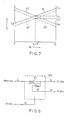
- a power source system comprises a power source (depicted at 85 in Fig. 13) substituted for each of the first and the second power sources 51 and 52 illustrated in Fig. 5.
- the power source 85 has first and second characteristic curves 86 and 87 (Fig. 12) when used as the first and the second power sources 51 and 52 (Fig. 5), respectively.
- each of the first and the second characteristic curves 86 and 87 partially shows a negative resistance characteristic like in Fig. 7 and is nonlinearly varied with an increase of each of the first and the second source voltages V A and V B .
- the first characteristic curve 86 shows a first resistance between zero and a transition voltage V t higher than the half (V L/ 2) of the load voltage and a second resistance between the transition voltage V t and the load voltage V L .
- the transition voltage V t is representative of a preselected rate of load sharing.
- the first resistance is a negative resistance and has a sufficiently small absolute value while the second resistance is a positive resistance.
- the second characteristic curve 87 is variable relative to the second source voltage V B in a manner similar to the first characteristic curve 86.
- lower limit characteristic curves 86' and 87' are illustrated in relation to the first and the second characteristic curves 86 and 87, respectively.
- the normal load current I L0 can approach the minimum current Imof the load 20 in comparison with that of the conventional power source system illustrated in Fig. 1. Accordingly, the load 20 may be small in size and inexpensive, as described in conjunction with Fig. 5.
- an increase of the load current I L can be reduced as compared with the power source system illustrated in Fig. 5 when a single one of the first and the second power sources alone is operated. This is because each of the first and the second d.c. currents I A and I B does not increase when each source voltage V A and V B exceeds the transition voltage V t .
- the power source 85 is assumed to be used as the first power source 51 and comprises a current detector 60' illustrated in Fig. 13. Any other elements and signals are similar to those illustrated in Figs. 5 and 6 and are therefore represented by the same reference numerals and symbols.
- the first current source 54a is operable in cooperation with the current detector 60' in a manner similar to that illustrated in Fig. 5 and produces the first d.c. current I A which is divided into the load current I L and the resistor current I R .
- the resistor current I R is supplied through the first resistor 56a to the current detector 60'.
- the current detector 60' comprises a magnetic amplifier depicted at 91.
- the illustrated magnetic amplifier 91 comprises a d.c. winding 92 and produces a detection signal having a detection voltage V d .
- the detection voltage V d is proportional to an ampere turn, namely, the resistor current I R .
- the detection voltage V d is sent to a limiter 94 for limiting the detection voltage V d when exceeds a prescribed reference voltage V 0 . More particularly, the limiter 94 produces the detection voltage V d as a control voltage V c when the detection voltage V d is not greater than the prescribed reference voltage V 0 . Otherwise, the limiter 94 produces the control voltage V c dependent on the prescribed reference voltage V 0 . Accordingly, the control voltage V c is generally represented by: where g 4 is indicative of a proportional constant.
- resistor current I R is represented by:
- Equation (23) represents the control voltage V c appearing when the first source voltage V A is not greater than the transition voltage V t .
- Equation (49') is rewritten with reference to Equations (20) through (22) into: It is noted here that Equation (24) is representative of the control voltage V c appearing when the first source voltage V A is greater than the transition voltage V t .
- the first current source 54a is supplied with the control voltage V c shown by Equation (23) or (24) and is subjected to current control in accordance with the control voltage V c .
- V c the control voltage
- the load current I L is represented by:
- Equation (26) it is possible to make a term of k 5 .g 5 greater than 1 and to make a term of R 10 /(k5 ⁇ g5-1) coincide with a desired value. Therefore, the negative resistance characteristic can be accomplished when the first d.c. voltage V A is not greater than the transition voltage V t , as shown at 86 in Fig. 12.
- the first resistor 56a and the current detector 60' are equivalent to a negative resistor and will collectively be called a control circuit 70 as mentioned before.
- Equation (27) the proportional constant g 4 is equal to zero when the limiter 94 is used in the current detector 60'. Equation (27) is simplified into:
- a power source system according to a fourth embodiment of this invention is similar to that illustrated in conjunction with Figs. 9 and 11 except that a power source 100 (Fig. 14) has a nonlinear characteristic as illustrated in Fig. 15 and is operable as each of the first and the second power sources 71 and 72 (Fig. 9).
- a power source 100 Fig. 14
- Fig. 9 the power source 100 illustrated in Fig. 14 is used as the first power source 71 (Fig. 9).
- a current detection circuit 76' in the power source 100 is similar to the current detector 60' illustrated in Fig. 13 and comprises a magnetic amplifier and a limiter which are indicated at 101 and 102, respectively, so as to provide a first one of the nonlinear characteristic indicated at 106 in Fig. 15. It is needless to say that a second one of the nonlinear characteristic 107 is given by the second power source 72 (Fig. 9).
- each of the first and the second nonlinear characteristics 106 and 107 has a transistion current It greater than a half of the load current I L , although the transition current It is illustrated only about the first nonlinear characteristic 106 in Fig. 15.
- the first d.c. voltage E A is developoed by the first voltage source 73a controllable in a manner to be described later.
- the first source current i A flows through the first diode 74a, the current detection circuit 76', and the first resistor 75a.
- the first source current i is combined with the second source current i (Fig. 9) to be supplied to the load 20 as the load current I L , as illustrated in Fig. 9.
- the first source current i A is detected by the current detection circuit 76'.
- the magnetic amplifier 101 produces a detection signal having a detection voltage V d in a manner similar to that illustrated in conjunction with Fig. 13.
- the detection voltage V d is therefore proportional to the first source current i A and is given by: where g 6 is representative of a proportional constant.
- the detection voltage V d is sent to the limiter 102 for limiting the detection voltage V d at a preselected reference voltage V 0 .
- the preselected reference voltage V 0 serves to provide the transition current I t .
- the limiter 102 may be called a comparing circuit.
- the comparing circuit produces a control voltage V c by comparing the detection voltage V d with the preselected reference voltage V 0 .
- V d ⁇ V 0 the comparing circuit produces the control voltage V c given by:
- the preselected reference voltage V 0 is determined in consideration of the transition current It and is given by:
- V d ⁇ V 0 namely, i A ⁇ I t
- V c the control voltage
- the first d.c. voltage E A of the first voltage source 73a is given by:
- the load voltage V L is equal to a difference between the first d.c. voltage E A and a voltage across the first resistor 75a and is represented with reference to Equations (29) to (31) by: and
- Equation (32) it is readily possible to make (k 6 ⁇ g 6 - R 20 ) a positive value. This means that the load voltage V L increases with an increment of the first source current i A when the first source current i A is not greater than I t . Therefore, the first nonlinear characteristic 106 partially has a negative resistance characteristic.
- Equation (33) it is possible to select the third term of (k 6 ⁇ g 6 ⁇ g 7 -R 20 ) so that a value of the term becomes equal to a desired value equal to or smaller than zero.
- the first nonlinear characteristic 106 can have a positive resistance characteristic when the first source current i A exceeds the transition current I t .
- a voltage detector may be used instead of each current detector illustrated in Figs. 5, 9, 13, and 14.
- the voltage detector may monitor a voltage across the resistor, such as 56, 75.
Landscapes
- Engineering & Computer Science (AREA)
- Physics & Mathematics (AREA)
- Electromagnetism (AREA)
- General Physics & Mathematics (AREA)
- Radar, Positioning & Navigation (AREA)
- Automation & Control Theory (AREA)
- Control Of Voltage And Current In General (AREA)
- Direct Current Feeding And Distribution (AREA)
Applications Claiming Priority (4)
| Application Number | Priority Date | Filing Date | Title |
|---|---|---|---|
| JP163090/84 | 1984-08-02 | ||
| JP163091/84 | 1984-08-02 | ||
| JP16309184A JPH0628006B2 (ja) | 1984-08-02 | 1984-08-02 | 負荷分担方式 |
| JP16309084A JPS6142230A (ja) | 1984-08-02 | 1984-08-02 | 負荷分担方式 |
Publications (3)
| Publication Number | Publication Date |
|---|---|
| EP0173104A2 true EP0173104A2 (de) | 1986-03-05 |
| EP0173104A3 EP0173104A3 (en) | 1987-07-15 |
| EP0173104B1 EP0173104B1 (de) | 1993-05-12 |
Family
ID=26488654
Family Applications (1)
| Application Number | Title | Priority Date | Filing Date |
|---|---|---|---|
| EP19850109654 Expired - Lifetime EP0173104B1 (de) | 1984-08-02 | 1985-08-01 | Energieversorgungsanordnung, bestehend aus einer Vielzahl von Energiequellen mit negativen Widerstandskarakteristiken |
Country Status (3)
| Country | Link |
|---|---|
| US (1) | US4728807A (de) |
| EP (1) | EP0173104B1 (de) |
| DE (1) | DE3587331T2 (de) |
Cited By (3)
| Publication number | Priority date | Publication date | Assignee | Title |
|---|---|---|---|---|
| GB2251096A (en) * | 1990-11-06 | 1992-06-24 | Measurement Tech Ltd | Loop power supply circuit |
| WO1996031818A1 (de) * | 1995-04-03 | 1996-10-10 | Siemens Nixdorf Informationssysteme Ag | Aufteilung von versorgungsströmen |
| KR101142095B1 (ko) * | 2008-01-25 | 2012-05-03 | 사우쓰 차이나 유니버시티 오브 테크놀로지 | 인장 유동학을 기초로 한 거대분자 물질의 가소화 방법과 운반 방법 및 장치 |
Families Citing this family (12)
| Publication number | Priority date | Publication date | Assignee | Title |
|---|---|---|---|---|
| FR2767933A1 (fr) * | 1997-08-27 | 1999-02-26 | Philips Electronics Nv | Circuit adaptateur de tension d'alimentation |
| DE19826958A1 (de) * | 1998-06-17 | 1999-12-23 | Lies Hans Dieter | Verfahren und Vorrichtung zum elektrochirurgischen Schneiden und Koagulieren |
| US7301313B1 (en) * | 1999-03-23 | 2007-11-27 | Intel Corporation | Multiple voltage regulators for use with a single load |
| JP2003504997A (ja) * | 1999-07-07 | 2003-02-04 | シンクォール・インコーポレーテッド | 同期整流器を備えたdc/dcパワー・コンバータの制御 |
| US6894468B1 (en) | 1999-07-07 | 2005-05-17 | Synqor, Inc. | Control of DC/DC converters having synchronous rectifiers |
| US6507129B2 (en) * | 2001-03-12 | 2003-01-14 | Celestica International Inc. | System and method for controlling an output signal of a power supply |
| US20050286191A1 (en) * | 2004-06-28 | 2005-12-29 | Pieter Vorenkamp | Power supply integrated circuit with multiple independent outputs |
| TWI558126B (zh) * | 2015-03-20 | 2016-11-11 | 瑞昱半導體股份有限公司 | 聯合供電模組及其系統 |
| US9977091B2 (en) * | 2015-04-28 | 2018-05-22 | Qualcomm Incorporated | Battery fuel gauges sharing current information between multiple battery chargers |
| US11848427B2 (en) * | 2017-12-07 | 2023-12-19 | Yazami Ip Pte. Ltd. | Non-linear voltammetry-based method for charging a battery and fast charging system implementing this method |
| CN111656643B (zh) | 2017-12-07 | 2024-11-15 | 雅扎米Ip私人有限公司 | 用于对电池快速充电的自适应充电协议和实现该协议的快速充电系统 |
| CN114172246B (zh) * | 2022-02-10 | 2022-04-26 | 中创新航科技股份有限公司 | 一种电池、电子设备及电池的充电方法 |
Family Cites Families (19)
| Publication number | Priority date | Publication date | Assignee | Title |
|---|---|---|---|---|
| GB959620A (en) * | 1962-05-11 | 1964-06-03 | Gen Electric Co Ltd | Improvements in or relating to electric circuits for supplying a substantially constant current to a load |
| US3293444A (en) * | 1962-09-05 | 1966-12-20 | United Aircraft Corp | Build-up circuit for series-connected power supplies |
| US3343067A (en) * | 1965-05-05 | 1967-09-19 | Lorain Prod Corp | Phase-controlling circuitry |
| US3428820A (en) * | 1966-05-19 | 1969-02-18 | Motorola Inc | Electroresponsive controls |
| US3696286A (en) * | 1970-08-06 | 1972-10-03 | North American Rockwell | System for detecting and utilizing the maximum available power from solar cells |
| US3689776A (en) * | 1970-08-25 | 1972-09-05 | Us Army | Isolation of parallel cell stacks in thermal batteries by a squib switch |
| US3738371A (en) * | 1970-12-11 | 1973-06-12 | Esb Inc | Cardiac pacers with source condition-responsive rate |
| US3768012A (en) * | 1972-05-08 | 1973-10-23 | Pioneer Magnetics Inc | Power supply current detector system |
| US3824450A (en) * | 1973-05-14 | 1974-07-16 | Rca Corp | Power supply keep alive system |
| US3808452A (en) * | 1973-06-04 | 1974-04-30 | Gte Automatic Electric Lab Inc | Power supply system having redundant d. c. power supplies |
| FR2246102B1 (de) * | 1973-09-27 | 1976-10-01 | Cit Alcatel | |
| US3912940A (en) * | 1974-09-18 | 1975-10-14 | Honeywell Inc | Dc power supply |
| US3956638A (en) * | 1974-12-20 | 1976-05-11 | Hughes Aircraft Company | Battery paralleling system |
| US4356403A (en) * | 1981-02-20 | 1982-10-26 | The Babcock & Wilcox Company | Masterless power supply arrangement |
| JPS5823488A (ja) * | 1981-08-06 | 1983-02-12 | Canon Inc | 太陽電池電源装置 |
| US4492919A (en) * | 1982-04-12 | 1985-01-08 | General Electric Company | Current sensors |
| JPS58215928A (ja) * | 1982-06-10 | 1983-12-15 | 富士電機株式会社 | 安定化電源の並列運転方式 |
| US4429233A (en) * | 1982-09-28 | 1984-01-31 | Reliance Electric Company | Synchronizing circuit for use in paralleled high frequency power supplies |
| JPH118543A (ja) * | 1997-06-18 | 1999-01-12 | Seiko Epson Corp | Cmos出力バッファ回路及びバイアス電圧発生回路 |
-
1985
- 1985-08-01 EP EP19850109654 patent/EP0173104B1/de not_active Expired - Lifetime
- 1985-08-01 DE DE8585109654T patent/DE3587331T2/de not_active Expired - Fee Related
- 1985-08-01 US US06/761,745 patent/US4728807A/en not_active Expired - Lifetime
Cited By (5)
| Publication number | Priority date | Publication date | Assignee | Title |
|---|---|---|---|---|
| GB2251096A (en) * | 1990-11-06 | 1992-06-24 | Measurement Tech Ltd | Loop power supply circuit |
| GB2251096B (en) * | 1990-11-06 | 1994-03-09 | Measurement Tech Ltd | Power supply circuits |
| WO1996031818A1 (de) * | 1995-04-03 | 1996-10-10 | Siemens Nixdorf Informationssysteme Ag | Aufteilung von versorgungsströmen |
| US5900724A (en) * | 1995-04-03 | 1999-05-04 | Siemens Nixdorf Informationssysteme Aktiengesellschaft | Method of splitting a power supply |
| KR101142095B1 (ko) * | 2008-01-25 | 2012-05-03 | 사우쓰 차이나 유니버시티 오브 테크놀로지 | 인장 유동학을 기초로 한 거대분자 물질의 가소화 방법과 운반 방법 및 장치 |
Also Published As
| Publication number | Publication date |
|---|---|
| DE3587331T2 (de) | 1993-08-19 |
| DE3587331D1 (de) | 1993-06-17 |
| US4728807A (en) | 1988-03-01 |
| EP0173104B1 (de) | 1993-05-12 |
| EP0173104A3 (en) | 1987-07-15 |
Similar Documents
| Publication | Publication Date | Title |
|---|---|---|
| EP0173104A2 (de) | Energieversorgungsanordnung, bestehend aus einer Vielzahl von Energiequellen mit negativen Widerstandskarakteristiken | |
| US4644458A (en) | Electric power supply circuit capable of reducing a loss of electric power | |
| CA1166689A (en) | "masterless" power supply arrangement | |
| US4720758A (en) | Load dependent current limiter for the power supply of a multi-module electronic system | |
| US4318007A (en) | Circuit arrangement for controlling the energization of a load from a plurality of current sources | |
| EP0723326A2 (de) | Batterieladegerät | |
| JPH06225453A (ja) | 電源システム | |
| US3723854A (en) | Circuit for compensating for line drop between power source and load circuit | |
| US4290007A (en) | High power and high voltage transistor control circuit | |
| US4578743A (en) | Converter control system having stable power transfer in the presence of decreased input AC voltage | |
| US3470442A (en) | Control systems for h.v.d.c. transmission links | |
| GB2086622A (en) | X-ray tube anode voltage compensator | |
| EP0204978B1 (de) | Steuergerät zum Ausserbetriebsetzen einer elektrischen Energieversorgung | |
| US2762964A (en) | Regulating control system | |
| EP0638857B1 (de) | Schaltung zur Verwendung mit einer Rückkopplungsanordnung | |
| US3996479A (en) | Comparator/bistable circuit | |
| US2522520A (en) | Control system for thyratrons | |
| JPS6051240B2 (ja) | X線装置 | |
| US3968372A (en) | Tube protection circuit for X-ray generators | |
| US2997643A (en) | Regulated direct current power supply | |
| EP0155074B1 (de) | Leitungsspeiseschaltung mit aktiver Impedanz und mit Erdschlussfehlerschutz | |
| EP0211507A1 (de) | Lastabhängiger Strombegrenzer für die Energieversorgung eines elektronischen Mehrmodulsystems | |
| JPH0756545Y2 (ja) | X線保護回路 | |
| SU1249661A1 (ru) | Способ управлени электронным вентилем | |
| SU1226587A1 (ru) | Устройство дл управлени электронно-лучевым вентилем |
Legal Events
| Date | Code | Title | Description |
|---|---|---|---|
| PUAI | Public reference made under article 153(3) epc to a published international application that has entered the european phase |
Free format text: ORIGINAL CODE: 0009012 |
|
| 17P | Request for examination filed |
Effective date: 19850801 |
|
| AK | Designated contracting states |
Kind code of ref document: A2 Designated state(s): DE FR GB |
|
| PUAL | Search report despatched |
Free format text: ORIGINAL CODE: 0009013 |
|
| AK | Designated contracting states |
Kind code of ref document: A3 Designated state(s): DE FR GB |
|
| 17Q | First examination report despatched |
Effective date: 19890817 |
|
| GRAA | (expected) grant |
Free format text: ORIGINAL CODE: 0009210 |
|
| AK | Designated contracting states |
Kind code of ref document: B1 Designated state(s): DE FR GB |
|
| REF | Corresponds to: |
Ref document number: 3587331 Country of ref document: DE Date of ref document: 19930617 |
|
| ET | Fr: translation filed | ||
| REG | Reference to a national code |
Ref country code: GB Ref legal event code: IF02 |
|
| PGFP | Annual fee paid to national office [announced via postgrant information from national office to epo] |
Ref country code: GB Payment date: 20020731 Year of fee payment: 18 |
|
| PGFP | Annual fee paid to national office [announced via postgrant information from national office to epo] |
Ref country code: DE Payment date: 20020807 Year of fee payment: 18 |
|
| PGFP | Annual fee paid to national office [announced via postgrant information from national office to epo] |
Ref country code: FR Payment date: 20020808 Year of fee payment: 18 |
|
| PG25 | Lapsed in a contracting state [announced via postgrant information from national office to epo] |
Ref country code: GB Free format text: LAPSE BECAUSE OF NON-PAYMENT OF DUE FEES Effective date: 20030801 |
|
| PG25 | Lapsed in a contracting state [announced via postgrant information from national office to epo] |
Ref country code: DE Free format text: LAPSE BECAUSE OF NON-PAYMENT OF DUE FEES Effective date: 20040302 |
|
| GBPC | Gb: european patent ceased through non-payment of renewal fee |
Effective date: 20030801 |
|
| PG25 | Lapsed in a contracting state [announced via postgrant information from national office to epo] |
Ref country code: FR Free format text: LAPSE BECAUSE OF NON-PAYMENT OF DUE FEES Effective date: 20040430 |
|
| REG | Reference to a national code |
Ref country code: FR Ref legal event code: ST |
|
| PLBE | No opposition filed within time limit |
Free format text: ORIGINAL CODE: 0009261 |
|
| STAA | Information on the status of an ep patent application or granted ep patent |
Free format text: STATUS: NO OPPOSITION FILED WITHIN TIME LIMIT |