EP0173611A2 - Procédé de formation auto-aligné de siliciure métallique pour circuits intégrés comportant des électrodes auto-alignées en silicium polycristallin - Google Patents
Procédé de formation auto-aligné de siliciure métallique pour circuits intégrés comportant des électrodes auto-alignées en silicium polycristallin Download PDFInfo
- Publication number
- EP0173611A2 EP0173611A2 EP85401539A EP85401539A EP0173611A2 EP 0173611 A2 EP0173611 A2 EP 0173611A2 EP 85401539 A EP85401539 A EP 85401539A EP 85401539 A EP85401539 A EP 85401539A EP 0173611 A2 EP0173611 A2 EP 0173611A2
- Authority
- EP
- European Patent Office
- Prior art keywords
- polycrystalline silicon
- layer
- silicon
- regions
- metal
- Prior art date
- Legal status (The legal status is an assumption and is not a legal conclusion. Google has not performed a legal analysis and makes no representation as to the accuracy of the status listed.)
- Withdrawn
Links
Images
Classifications
-
- H—ELECTRICITY
- H10—SEMICONDUCTOR DEVICES; ELECTRIC SOLID-STATE DEVICES NOT OTHERWISE PROVIDED FOR
- H10D—INORGANIC ELECTRIC SEMICONDUCTOR DEVICES
- H10D1/00—Resistors, capacitors or inductors
- H10D1/40—Resistors
- H10D1/47—Resistors having no potential barriers
-
- H—ELECTRICITY
- H10—SEMICONDUCTOR DEVICES; ELECTRIC SOLID-STATE DEVICES NOT OTHERWISE PROVIDED FOR
- H10D—INORGANIC ELECTRIC SEMICONDUCTOR DEVICES
- H10D62/00—Semiconductor bodies, or regions thereof, of devices having potential barriers
- H10D62/40—Crystalline structures
-
- H—ELECTRICITY
- H10—SEMICONDUCTOR DEVICES; ELECTRIC SOLID-STATE DEVICES NOT OTHERWISE PROVIDED FOR
- H10D—INORGANIC ELECTRIC SEMICONDUCTOR DEVICES
- H10D64/00—Electrodes of devices having potential barriers
- H10D64/01—Manufacture or treatment
- H10D64/011—Manufacture or treatment of electrodes ohmically coupled to a semiconductor
- H10D64/0111—Manufacture or treatment of electrodes ohmically coupled to a semiconductor to Group IV semiconductors
- H10D64/0113—Manufacture or treatment of electrodes ohmically coupled to a semiconductor to Group IV semiconductors the conductive layers comprising highly doped semiconductor materials, e.g. polysilicon layers or amorphous silicon layers
-
- H—ELECTRICITY
- H10—SEMICONDUCTOR DEVICES; ELECTRIC SOLID-STATE DEVICES NOT OTHERWISE PROVIDED FOR
- H10P—GENERIC PROCESSES OR APPARATUS FOR THE MANUFACTURE OR TREATMENT OF DEVICES COVERED BY CLASS H10
- H10P32/00—Diffusion of dopants within, into or out of wafers, substrates or parts of devices
- H10P32/10—Diffusion of dopants within, into or out of semiconductor bodies or layers
- H10P32/14—Diffusion of dopants within, into or out of semiconductor bodies or layers within a single semiconductor body or layer in a solid phase; between different semiconductor bodies or layers, both in a solid phase
- H10P32/1408—Diffusion of dopants within, into or out of semiconductor bodies or layers within a single semiconductor body or layer in a solid phase; between different semiconductor bodies or layers, both in a solid phase from or through or into an external applied layer, e.g. photoresist or nitride layers
- H10P32/1414—Diffusion of dopants within, into or out of semiconductor bodies or layers within a single semiconductor body or layer in a solid phase; between different semiconductor bodies or layers, both in a solid phase from or through or into an external applied layer, e.g. photoresist or nitride layers the applied layer being silicon, silicide or SIPOS, e.g. polysilicon or porous silicon
-
- H—ELECTRICITY
- H10—SEMICONDUCTOR DEVICES; ELECTRIC SOLID-STATE DEVICES NOT OTHERWISE PROVIDED FOR
- H10P—GENERIC PROCESSES OR APPARATUS FOR THE MANUFACTURE OR TREATMENT OF DEVICES COVERED BY CLASS H10
- H10P32/00—Diffusion of dopants within, into or out of wafers, substrates or parts of devices
- H10P32/10—Diffusion of dopants within, into or out of semiconductor bodies or layers
- H10P32/17—Diffusion of dopants within, into or out of semiconductor bodies or layers characterised by the semiconductor material
- H10P32/171—Diffusion of dopants within, into or out of semiconductor bodies or layers characterised by the semiconductor material being group IV material
Definitions
- This invention relates to integrated circuit fabrication processes, and in particular, to a method of providing self-aligned metal silicide layers on bipolar integrated circuits which circuits also include self-aligned polycrystalline silicon features such as electrodes.
- Prior art processes for fabricating bipolar integrated circuits having self-aligned polycrystalline silicon electrodes and layers of metal silicide to provide interconnections suffer from several disadvantages.
- the dopant used to fabricate the base contact, emitter, and other regions must be contained in the polycrystalline silicon if the polysilicon electrodes are to be self-aligned, the dopant is prone to migrate into the overlying layers of metal silicide during the thermal processes used to diffuse the dopant.
- an etching step must be performed to remove undesired regions of metal silicide from the wafer.
- This step is not only desirable because of the extra process complexity, but also because it leaves traces of unetchable conductive residues on the field oxide areas. These traces increase the emitter-base and collector-base junction leakages, thereby substantially degrading circuit performance. Furthermore, because such prior art processes typically required long annealing treatments to lower sufficiently the resistance of the fabricated metal silicide layers, metal oxidation and incorporation of oxygen into the silicide film were common occurrences.
- the process of this invention includes the steps of depositing a layer of polycrystalline silicon across the upper surface of a semiconductor substrate, patterning the layer of polycrystalline silicon to form electrodes such as to contact ohmically emitters, base contacts, resistors, and diodes; heating the structure to cause impurity dopant in the polycrystalline silicon to diffuse into the semiconductor structure; protecting those portions of the structure where metal silicide is not desired; depositing metal across the structure; and reacting the metal with the underlying structure wherever metal silicide is to be formed.
- the step of patterning the polycrystalline silicon layer includes depositing a layer of silicon nitride across a sheet of polycrystalline silicon, patterning the nitride layer, then using photoresist and the nitride layer to mask all of the polycrystalline silicon layer except those portions to be removed. Also in the preferred embodiment the step of protecting the regions where silicide is not desired comprises oxidizing those regions to form a protective layer of silicon dioxide.
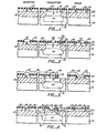
- Figure 1 is a cross-sectional view of a partially completed integrated circuit structure.
- the structure shown in Figure 1 includes a monocrystalline silicon substrate 10 in which an n conductivity type buried layer 15 has been formed.
- An epitaxial silicon layer 18 has been deposited across the surface of substrate 10 and oxidized isolation regions 12 formed. Regions 12, 15, and 18 may be fabricated using well-known semiconductor process technology, for example, as set forth in the Peltzer patent above.
- a layer of polycrystalline silicon 20 of desired thickness is deposited, for example, using chemical vapor deposition technology.
- desired conductivity impurities such as arsenic, boron, or phosphorous, are introduced into layer 20 to dope desired regions of the layer.
- desired conductivity impurities such as arsenic, boron, or phosphorous
- the particular pattern and arrangement of these doped regions will be dependent upon the desired active and/or passive devices to be fabricated in the epitaxial silicon 18 and in the polycrystalline silicon 20.
- Figure 1 has been divided into thirds, and the application of the process of this invention will be described in conjunction with the fabrication of a resistor, a transistor, and a diode.
- resistor, and electrical contacts thereto are fabricated in the manner depicted in the left-hand third of each figure, while the diode, and the application of the process of this invention thereto, is depicted in the right-hand third of the figures.
- the center of each of Figures 1-7 is used to depict the fabrication of a transistor.
- region 21 of layer 20 has been lightly doped with n conductivity type impurity to begin the fabrication of a resistor.
- Region 22 has been heavily doped with p conductivity type impurity and will provide an ohmic connection to a self-aligned transistor base contact fabricated beneath it. The base contact will enable an electrical connection to be made to region 18, which will become the base of a vertical npn transistor.
- N conductivity type region 24 will be used for the fabrication of a self-aligned emitter/emitter contact for the transistor.
- P type region 25 and n type region 26 together will provide a diode for the integrated circuit.
- nitride layer 30 is deposited using chemical vapor deposition to a thickness of about 1000 angstroms.
- the structure is then masked using well-known photolithographic techniques and these undesired portions of layer 30 removed, as shown by Figure 2.
- Silicon nitride layer 30 will be removed wherever an electrically conductive to-be-formed layer of metal silicide is not desired. For example, in Figure 2 an opening 31 is created above region 21 because a silicide layer is not desired there (and if placed there would short out the to-be-formed resistor.)
- the nitride 30 is removed from region-34 to prevent fabrication of metal silicide in this region which would short pn junction 35 destroying the diode.
- the layer of polycrystalline silicon 20 is intact and extends across the entire upper surface of the integrated circuit structure.
- the silicon nitride is etched using well-known techniques.
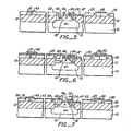
- a layer of photoresist 40 is deposited across the upper surface of the structure and removed from regions where underlying polycrystalline silicon is to be removed.
- the photoresist layer 40 will prevent etching of the polycrystalline silicon regions 21 as well as regions 25 and 26 otherwise exposed through opening 34.
- the nitride is etched with C 2 F 6 and helium plasma in a Sigma 80 reactor.
- the resist 40 will serve to define the sheet of polycrystalline silicon 20 into a series of polycrystalline lines rather than a single sheet. The length of the lines runs in the direction of the width of the Figures, while the width of the lines extends into the page, perpendicular to both the thickness and length.
- the polycrystalline silicon is etched in a LAM etcher using carbon tetrachloride and helium.
- the structure is heated to diffuse impurity out of the polycrystalline silicon regions into to the underlying silicon.
- a base contact 42 has been formed in this manner beneath polysilicon 22, while an emitter 44 is formed beneath contact 24.
- the particular parameters of the thermal drive-in process will depend upon the desired characteristics of the resulting transistor. In one embodiment a temperature of 950°C for 30 minutes has been found satisfactory. This process will also activate the dopants in the polycrystalline silicon and render it conductive. For example, prior to the thermal process the polycrystalline silicon will have essentially an infinite resistance, while afterward the resistance usually will be on the order of 50 ohms per square, depending upon the impurity concentration in the polysilicon 20.
- the structure is thermally oxidized to passivate the active areas and the sidewalls of the polysilicon lines 20.
- a layer of silicon dioxide 45 is formed on the upper surface of resistor 21 and a layer of silicon dioxide 46 is formed on epitaxial silicon 18 and the sidewalls of polysilicon regions 22 and 24.
- Silicon dioxide 47 is formed on the other side of polysilicon 24, while silicon dioxide layer 48 is formed on the upper surface of the diode. Not shown in the figures, but formed at the same time, will be a layer of silicon dioxide along the exposed sides of the entire polysilicon line 20.
- the remaining silicon nitride 30 is then removed to create the structure shown in Figure 5.
- This silicon nitride may be removed by dipping the entire structure in hot phosphoric acid (H 3 P0 4 ) at a temperature of about 150°C. This etch will not effect the polycrystalline silicon or the silicon dioxide.
- a relatively thin layer of a refractory metal such as titanium, molybdenum or tungsten is deposited.
- the metal is deposited in a substantially pure form at a relatively low temperature, for example, using RF sputtering. In the preferred embodiment approximately 600 Angstroms of titanium are deposited.
- the integrated circuit structure is then placed in a Heatpulse reactor, manufactured by A.G. Associates in Palo Alto, California and heated in an nitrogen ambient for approximately 10 seconds to approximately 800°C.
- a Heatpulse reactor manufactured by A.G. Associates in Palo Alto, California and heated in an nitrogen ambient for approximately 10 seconds to approximately 800°C.
- This process is described in more detail in United States Patent application serial number 634,937 entitled: Improved Method To Control Lateral Silicon Diffusion In A Self-Aligned TiSi 2 Process and filed the same date as this application. Both applications are commonly assigned to Fairchild Camera & Instrument Corporation.
- titanium silicide will be formed everywhere titanium 50 has been deposited on polysilicon, but will not be formed anywhere the metal has been deposited on silicon dioxide.
- the fabrication of titanium silicide regions on the semiconductor structure is self-aligned to the polycrystalline silicon regions underlying the silicide.
- silicide By fabrication of the silicide using the technique described in the above-referenced co-pending application, silicon from the underlying polycrystalline silicon does not diffuse to any significant extent through the metal to create undesired regions of silicide. Because the combined volume of metal and polycrystalline silicon prior to the reaction is greater than the resulting volume of metal silicide, the silicide will tend to be inset into the underlying polycrystalline silicon, as shown by Figure 7.
- the remaining titanium is selectively etched away in a solution of ammonium hydroxide (NH 4 0H) and hydrogen peroxide (H 2 0 2 ) (1:3 by volume).
- the solution dissolves titanium but does not dissolve titanium silicide.
- the same solution can be used to remove unreacted tungsten if tungsten silicide is to be formed instead of titanium silicide.
- phosphoric acid H 3 P0 4
- the structure is again heated to lower the sheet resistance of the silicide.
- silicide regions 52 and 53 provide electrical connections to the lightly doped polysilicon region 21, thereby forming a resistor.
- Silicide region 54 is deposited upon base contact electrode 22 to provide a low resistance connection to base 18 via contact 42.
- Silicide 55 on emitter contact 24 provides a connection to emitter region 44.
- Silicide regions 57 and 58 provide electrical connections to the diode formed at the interface of polycrystalline silicon regions 25 and 26.
- the structure shown in Figure 7 may be subjected to further well-known integrated circuit processes to create additional layers of interconnections.
- passivating material may be deposited across the entire upper surface of the integrated circuit, openings formed therein, and a layer of metal deposited thereon to provide connections to the silicide regions shown.
- the silicon dioxide regions 45, 46, 47, and 48 prevent inadvertent connections to resistor 21, base 18, and the diode 25/26.
- the process of this invention permits fabrication of these critical circuit elements and integration of them into an integrated circuit without the disadvantages of prior art processes.
- the process of this invention minimizes the movement of dopants into the silicide from the polycrystalline silicon, which would occur if the junction drive-in step followed the silicide formation as in the prior art.
- the process eliminates the metallic contaminants which often led to high device leakage currents, by eliminating the need to etch the completed silicide layer.
- the very short time required to anneal the structure greatly reduces the risk of oxidizing any metal in the integrated circuit and prevents the incorporation of oxygen into the titanium silicide which was a common occurrence in conventional prior art processes.
Landscapes
- Bipolar Transistors (AREA)
- Electrodes Of Semiconductors (AREA)
- Internal Circuitry In Semiconductor Integrated Circuit Devices (AREA)
- Semiconductor Integrated Circuits (AREA)
Applications Claiming Priority (2)
| Application Number | Priority Date | Filing Date | Title |
|---|---|---|---|
| US634936 | 1984-07-27 | ||
| US06/634,936 US4609568A (en) | 1984-07-27 | 1984-07-27 | Self-aligned metal silicide process for integrated circuits having self-aligned polycrystalline silicon electrodes |
Publications (2)
| Publication Number | Publication Date |
|---|---|
| EP0173611A2 true EP0173611A2 (fr) | 1986-03-05 |
| EP0173611A3 EP0173611A3 (fr) | 1988-01-20 |
Family
ID=24545755
Family Applications (1)
| Application Number | Title | Priority Date | Filing Date |
|---|---|---|---|
| EP85401539A Withdrawn EP0173611A3 (fr) | 1984-07-27 | 1985-07-26 | Procédé de formation auto-aligné de siliciure métallique pour circuits intégrés comportant des électrodes auto-alignées en silicium polycristallin |
Country Status (4)
| Country | Link |
|---|---|
| US (1) | US4609568A (fr) |
| EP (1) | EP0173611A3 (fr) |
| JP (1) | JPS6187368A (fr) |
| CA (1) | CA1241770A (fr) |
Cited By (3)
| Publication number | Priority date | Publication date | Assignee | Title |
|---|---|---|---|---|
| FR2607629A1 (fr) * | 1986-11-28 | 1988-06-03 | Fuji Electric Co Ltd | Procede de fabrication d'un transistor a haute tension |
| EP0258147A3 (fr) * | 1986-08-28 | 1988-08-10 | Fairchild Semiconductor Corporation | Procédé pour fabriquer un transistor du type bipolaire comportant un ruban en polysilicium |
| EP0418670A3 (en) * | 1989-09-19 | 1992-04-15 | National Semiconductor Corporation | Process for fabricating high performance bimos circuits |
Families Citing this family (53)
| Publication number | Priority date | Publication date | Assignee | Title |
|---|---|---|---|---|
| US5227316A (en) * | 1985-01-22 | 1993-07-13 | National Semiconductor Corporation | Method of forming self aligned extended base contact for a bipolar transistor having reduced cell size |
| US5045916A (en) * | 1985-01-22 | 1991-09-03 | Fairchild Semiconductor Corporation | Extended silicide and external contact technology |
| US5061986A (en) * | 1985-01-22 | 1991-10-29 | National Semiconductor Corporation | Self-aligned extended base contact for a bipolar transistor having reduced cell size and improved electrical characteristics |
| US5100824A (en) * | 1985-04-01 | 1992-03-31 | National Semiconductor Corporation | Method of making small contactless RAM cell |
| US5340762A (en) * | 1985-04-01 | 1994-08-23 | Fairchild Semiconductor Corporation | Method of making small contactless RAM cell |
| US5072275A (en) * | 1986-02-28 | 1991-12-10 | Fairchild Semiconductor Corporation | Small contactless RAM cell |
| US4663191A (en) * | 1985-10-25 | 1987-05-05 | International Business Machines Corporation | Salicide process for forming low sheet resistance doped silicon junctions |
| US5063168A (en) * | 1986-07-02 | 1991-11-05 | National Semiconductor Corporation | Process for making bipolar transistor with polysilicon stringer base contact |
| US4974046A (en) * | 1986-07-02 | 1990-11-27 | National Seimconductor Corporation | Bipolar transistor with polysilicon stringer base contact |
| US4929570A (en) * | 1986-10-06 | 1990-05-29 | National Semiconductor Corporation | Selective epitaxy BiCMOS process |
| US4849344A (en) * | 1986-12-11 | 1989-07-18 | Fairchild Semiconductor Corporation | Enhanced density modified isoplanar process |
| US4816423A (en) * | 1987-05-01 | 1989-03-28 | Texas Instruments Incorporated | Bicmos process for forming shallow npn emitters and mosfet source/drains |
| US5059546A (en) * | 1987-05-01 | 1991-10-22 | Texas Instruments Incorporated | BICMOS process for forming shallow NPN emitters and mosfet source/drains |
| US5354699A (en) * | 1987-05-13 | 1994-10-11 | Hitachi, Ltd. | Method of manufacturing semiconductor integrated circuit device |
| US5014107A (en) * | 1987-07-29 | 1991-05-07 | Fairchild Semiconductor Corporation | Process for fabricating complementary contactless vertical bipolar transistors |
| US4803175A (en) * | 1987-09-14 | 1989-02-07 | Motorola Inc. | Method of fabricating a bipolar semiconductor device with silicide contacts |
| US5089429A (en) * | 1989-06-22 | 1992-02-18 | David Sarnoff Research Center, Inc. | Self-aligned emitter bicmos process |
| US5107320A (en) * | 1989-08-09 | 1992-04-21 | National Semiconductor Corporation | Method and apparatus for improvement of interconnection capacitance |
| US5262672A (en) * | 1989-08-09 | 1993-11-16 | National Semiconductor Corporation | Apparatus for improvement of interconnection capacitance |
| US5234847A (en) * | 1990-04-02 | 1993-08-10 | National Semiconductor Corporation | Method of fabricating a BiCMOS device having closely spaced contacts |
| US5139961A (en) * | 1990-04-02 | 1992-08-18 | National Semiconductor Corporation | Reducing base resistance of a bjt by forming a self aligned silicide in the single crystal region of the extrinsic base |
| KR100234550B1 (ko) * | 1990-04-02 | 1999-12-15 | 클라크 3세 존 엠 | 증가된 항복 전압을 지닌 트랜지스터 디바이스 및 제조방법 |
| US5045483A (en) * | 1990-04-02 | 1991-09-03 | National Semiconductor Corporation | Self-aligned silicided base bipolar transistor and resistor and method of fabrication |
| EP0452720A3 (en) * | 1990-04-02 | 1994-10-26 | Nat Semiconductor Corp | A semiconductor structure and method of its manufacture |
| EP0450503A3 (en) * | 1990-04-02 | 1992-05-20 | National Semiconductor Corporation | Semiconductor devices with borosilicate glass sidewall spacers and method of fabrication |
| US5139966A (en) * | 1990-04-02 | 1992-08-18 | National Semiconductor Corporation | Low resistance silicided substrate contact |
| US5219784A (en) * | 1990-04-02 | 1993-06-15 | National Semiconductor Corporation | Spacer formation in a bicmos device |
| US5231042A (en) * | 1990-04-02 | 1993-07-27 | National Semiconductor Corporation | Formation of silicide contacts using a sidewall oxide process |
| US5107321A (en) * | 1990-04-02 | 1992-04-21 | National Semiconductor Corporation | Interconnect method for semiconductor devices |
| US5242854A (en) * | 1990-04-02 | 1993-09-07 | National Semiconductor Corporation | High performance semiconductor devices and their manufacture |
| US5079182A (en) * | 1990-04-02 | 1992-01-07 | National Semiconductor Corporation | Bicmos device having self-aligned well tap and method of fabrication |
| US5151387A (en) * | 1990-04-30 | 1992-09-29 | Sgs-Thomson Microelectronics, Inc. | Polycrystalline silicon contact structure |
| US5068201A (en) * | 1990-05-31 | 1991-11-26 | Sgs-Thomson Microelectronics, Inc. | Method for forming a high valued resistive load element and low resistance interconnect for integrated circuits |
| US5071778A (en) * | 1990-06-26 | 1991-12-10 | National Semiconductor Corporation | Self-aligned collector implant for bipolar transistors |
| US5289024A (en) * | 1990-08-07 | 1994-02-22 | National Semiconductor Corporation | Bipolar transistor with diffusion compensation |
| US5225359A (en) * | 1990-08-17 | 1993-07-06 | National Semiconductor Corporation | Method of fabricating Schottky barrier diodes and Schottky barrier diode-clamped transistors |
| US5109256A (en) * | 1990-08-17 | 1992-04-28 | National Semiconductor Corporation | Schottky barrier diodes and Schottky barrier diode-clamped transistors and method of fabrication |
| EP0490236A3 (en) * | 1990-12-13 | 1992-08-12 | National Semiconductor Corporation | Fabrication process for schottky barrier diodes on a substrate |
| US5169794A (en) * | 1991-03-22 | 1992-12-08 | National Semiconductor Corporation | Method of fabrication of pnp structure in a common substrate containing npn or MOS structures |
| US5462894A (en) * | 1991-08-06 | 1995-10-31 | Sgs-Thomson Microelectronics, Inc. | Method for fabricating a polycrystalline silicon resistive load element in an integrated circuit |
| JP2705476B2 (ja) * | 1992-08-07 | 1998-01-28 | ヤマハ株式会社 | 半導体装置の製造方法 |
| US5286991A (en) * | 1992-08-26 | 1994-02-15 | Pioneer Semiconductor Corporation | Capacitor for a BiCMOS device |
| US5325268A (en) * | 1993-01-28 | 1994-06-28 | National Semiconductor Corporation | Interconnector for a multi-chip module or package |
| JP3249292B2 (ja) * | 1994-04-28 | 2002-01-21 | 株式会社リコー | デュアルゲート構造の相補形mis半導体装置 |
| JPH0831841A (ja) | 1994-07-12 | 1996-02-02 | Sony Corp | 半導体装置及びその製造方法 |
| JP3297784B2 (ja) * | 1994-09-29 | 2002-07-02 | ソニー株式会社 | 拡散層抵抗の形成方法 |
| US5888903A (en) * | 1995-06-07 | 1999-03-30 | Texas Instruments Incorporated | Self-aligned silicide process |
| US6188136B1 (en) * | 1996-06-26 | 2001-02-13 | Kabushiki Kaisha Toshiba | Semiconductor device including a wiring layer having a non-doped or high resistivity polycrystal silicon portion |
| US6143613A (en) * | 1997-06-30 | 2000-11-07 | Vlsi Technology, Inc. | Selective exclusion of silicide formation to make polysilicon resistors |
| JPH11195711A (ja) * | 1997-10-27 | 1999-07-21 | Seiko Epson Corp | 半導体装置およびその製造方法 |
| JPH11195753A (ja) | 1997-10-27 | 1999-07-21 | Seiko Epson Corp | 半導体装置およびその製造方法 |
| US6690083B1 (en) * | 2000-06-01 | 2004-02-10 | Koninklijke Philips Electronics N.V. | Use of silicide blocking layer to create high valued resistor and diode for sub-1V bandgap |
| CN110335818B (zh) * | 2019-05-23 | 2022-11-18 | 福建省福联集成电路有限公司 | 一种异质结双极晶体管结构及制造方法 |
Family Cites Families (7)
| Publication number | Priority date | Publication date | Assignee | Title |
|---|---|---|---|---|
| US3777364A (en) * | 1972-07-31 | 1973-12-11 | Fairchild Camera Instr Co | Methods for forming metal/metal silicide semiconductor device interconnect system |
| NL7510903A (nl) * | 1975-09-17 | 1977-03-21 | Philips Nv | Werkwijze voor het vervaardigen van een halfgelei- derinrichting, en inrichting vervaardigd volgens de werkwijze. |
| FR2340619A1 (fr) * | 1976-02-04 | 1977-09-02 | Radiotechnique Compelec | Perfectionnement au procede de fabrication de dispositifs semiconducteurs et dispositifs ainsi obtenus |
| US4249968A (en) * | 1978-12-29 | 1981-02-10 | International Business Machines Corporation | Method of manufacturing a metal-insulator-semiconductor utilizing a multiple stage deposition of polycrystalline layers |
| US4305200A (en) * | 1979-11-06 | 1981-12-15 | Hewlett-Packard Company | Method of forming self-registering source, drain, and gate contacts for FET transistor structures |
| JPS5748246A (en) * | 1980-08-13 | 1982-03-19 | Fujitsu Ltd | Manufacture of semiconductor device |
| DE3334774A1 (de) * | 1983-09-26 | 1985-04-11 | Siemens AG, 1000 Berlin und 8000 München | Integrierbarer npn-transistor |
-
1984
- 1984-07-27 US US06/634,936 patent/US4609568A/en not_active Expired - Lifetime
-
1985
- 1985-07-26 EP EP85401539A patent/EP0173611A3/fr not_active Withdrawn
- 1985-07-26 CA CA000487618A patent/CA1241770A/fr not_active Expired
- 1985-07-26 JP JP60164195A patent/JPS6187368A/ja active Pending
Cited By (4)
| Publication number | Priority date | Publication date | Assignee | Title |
|---|---|---|---|---|
| EP0258147A3 (fr) * | 1986-08-28 | 1988-08-10 | Fairchild Semiconductor Corporation | Procédé pour fabriquer un transistor du type bipolaire comportant un ruban en polysilicium |
| FR2607629A1 (fr) * | 1986-11-28 | 1988-06-03 | Fuji Electric Co Ltd | Procede de fabrication d'un transistor a haute tension |
| US4892839A (en) * | 1986-11-28 | 1990-01-09 | Fuji Electric Co., Ltd. | Method of manufacturing a semiconductor device with polysilicon resistors and field plate |
| EP0418670A3 (en) * | 1989-09-19 | 1992-04-15 | National Semiconductor Corporation | Process for fabricating high performance bimos circuits |
Also Published As
| Publication number | Publication date |
|---|---|
| EP0173611A3 (fr) | 1988-01-20 |
| JPS6187368A (ja) | 1986-05-02 |
| US4609568A (en) | 1986-09-02 |
| CA1241770A (fr) | 1988-09-06 |
Similar Documents
| Publication | Publication Date | Title |
|---|---|---|
| US4609568A (en) | Self-aligned metal silicide process for integrated circuits having self-aligned polycrystalline silicon electrodes | |
| US4528744A (en) | Method of manufacturing a semiconductor device | |
| US4433468A (en) | Method for making semiconductor device having improved thermal stress characteristics | |
| EP0052450B1 (fr) | Procédé de fabrication d'un dispositif semiconducteur comprenant des électrodes en semiconducteur polycristallin et métal | |
| US4486942A (en) | Method of manufacturing semiconductor integrated circuit BI-MOS device | |
| EP0188291B1 (fr) | Dispositif semi-conducteur bipolaire et son procédé de fabrication | |
| EP0170250B1 (fr) | Transistor bipolaire et son procédé de fabrication | |
| JPS62588B2 (fr) | ||
| KR940009360B1 (ko) | 반도체장치 및 그 제조방법 | |
| KR100196085B1 (ko) | 고성능 반도체 디바이스 및 그 제조 방법 | |
| EP0112773B1 (fr) | Transistor comportant une structure Schottky enterrée de limitation | |
| JP3098848B2 (ja) | 自己整合型プレーナモノリシック集積回路縦型トランジスタプロセス | |
| EP0314600A2 (fr) | Emetteur auto-aligné en polysilicium et structure de contact pour un transistor bipolaire haute performance | |
| JPS61180482A (ja) | バイポーラトランジスタを製造する方法 | |
| EP0078220B1 (fr) | Interférences de silicium polycristallin pour transistors bipolaires en circuit flip-flop | |
| EP0030147A1 (fr) | Procédé de fabrication d'un circuit intégré à semi-conducteur | |
| US4691436A (en) | Method for fabricating a bipolar semiconductor device by undercutting and local oxidation | |
| EP0732746B1 (fr) | Procédé de fabrication d'un circuit intégré à transistors bipolaires complémentaires | |
| US4883772A (en) | Process for making a self-aligned silicide shunt | |
| US5151378A (en) | Self-aligned planar monolithic integrated circuit vertical transistor process | |
| KR100300892B1 (ko) | 반도체장치제조방법 | |
| US3925105A (en) | Process for fabricating integrated circuits utilizing ion implantation | |
| US4653173A (en) | Method of manufacturing an insulated gate field effect device | |
| US6919615B2 (en) | Semiconductor device for integrated injection logic cell and process for fabricating the same | |
| EP0264309B1 (fr) | Shunt de base auto-aligné pour un transistor |
Legal Events
| Date | Code | Title | Description |
|---|---|---|---|
| PUAI | Public reference made under article 153(3) epc to a published international application that has entered the european phase |
Free format text: ORIGINAL CODE: 0009012 |
|
| AK | Designated contracting states |
Kind code of ref document: A2 Designated state(s): DE FR GB IT NL |
|
| PUAL | Search report despatched |
Free format text: ORIGINAL CODE: 0009013 |
|
| AK | Designated contracting states |
Kind code of ref document: A3 Designated state(s): DE FR GB IT NL |
|
| RAP1 | Party data changed (applicant data changed or rights of an application transferred) |
Owner name: FAIRCHILD SEMICONDUCTOR CORPORATION |
|
| 17P | Request for examination filed |
Effective date: 19880716 |
|
| 17Q | First examination report despatched |
Effective date: 19891010 |
|
| STAA | Information on the status of an ep patent application or granted ep patent |
Free format text: STATUS: THE APPLICATION IS DEEMED TO BE WITHDRAWN |
|
| 18D | Application deemed to be withdrawn |
Effective date: 19900421 |
|
| RIN1 | Information on inventor provided before grant (corrected) |
Inventor name: VORA, MADHU Inventor name: CHIEN, FRANK Inventor name: KOH, YUN BAI |