EP0174372A1 - Stromquelle für elektrische entladungsbearbeitung - Google Patents
Stromquelle für elektrische entladungsbearbeitung Download PDFInfo
- Publication number
- EP0174372A1 EP0174372A1 EP85901056A EP85901056A EP0174372A1 EP 0174372 A1 EP0174372 A1 EP 0174372A1 EP 85901056 A EP85901056 A EP 85901056A EP 85901056 A EP85901056 A EP 85901056A EP 0174372 A1 EP0174372 A1 EP 0174372A1
- Authority
- EP
- European Patent Office
- Prior art keywords
- charging
- capacitor
- power source
- electric discharge
- discharging
- Prior art date
- Legal status (The legal status is an assumption and is not a legal conclusion. Google has not performed a legal analysis and makes no representation as to the accuracy of the status listed.)
- Granted
Links
- 238000003754 machining Methods 0.000 title claims abstract description 18
- 239000003990 capacitor Substances 0.000 claims abstract description 49
- 238000007599 discharging Methods 0.000 claims abstract description 23
- 238000009499 grossing Methods 0.000 claims abstract description 5
- 230000003247 decreasing effect Effects 0.000 description 5
- 238000010586 diagram Methods 0.000 description 2
- 230000017525 heat dissipation Effects 0.000 description 2
- 239000002184 metal Substances 0.000 description 1
Images

Classifications
-
- B—PERFORMING OPERATIONS; TRANSPORTING
- B23—MACHINE TOOLS; METAL-WORKING NOT OTHERWISE PROVIDED FOR
- B23H—WORKING OF METAL BY THE ACTION OF A HIGH CONCENTRATION OF ELECTRIC CURRENT ON A WORKPIECE USING AN ELECTRODE WHICH TAKES THE PLACE OF A TOOL; SUCH WORKING COMBINED WITH OTHER FORMS OF WORKING OF METAL
- B23H1/00—Electrical discharge machining, i.e. removing metal with a series of rapidly recurring electrical discharges between an electrode and a workpiece in the presence of a fluid dielectric
- B23H1/02—Electric circuits specially adapted therefor, e.g. power supply, control, preventing short circuits or other abnormal discharges
- B23H1/022—Electric circuits specially adapted therefor, e.g. power supply, control, preventing short circuits or other abnormal discharges for shaping the discharge pulse train
-
- B—PERFORMING OPERATIONS; TRANSPORTING
- B23—MACHINE TOOLS; METAL-WORKING NOT OTHERWISE PROVIDED FOR
- B23H—WORKING OF METAL BY THE ACTION OF A HIGH CONCENTRATION OF ELECTRIC CURRENT ON A WORKPIECE USING AN ELECTRODE WHICH TAKES THE PLACE OF A TOOL; SUCH WORKING COMBINED WITH OTHER FORMS OF WORKING OF METAL
- B23H2300/00—Power source circuits or energization
- B23H2300/20—Relaxation circuit power supplies for supplying the machining current, e.g. capacitor or inductance energy storage circuits
Definitions
- the present invention relates to a power source for an electric discharge machine such as a die sinking type electric discharge machine or a wire type electric discharge machine for machining a metal or the like by using discharge energy from a capacitor.
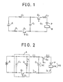
- FIG. 1 A conventional power source circuit for an electric discharge machining power source for performing machining by discharge of the capacitor is illustrated in Fig. 1.
- reference symbol E denotes a power source
- Rl a current limiting resistor
- C1 a charging/discharging capacitor
- P an electrode
- W a workpiece
- Q1 a transistor as a switching element for charging the capacitor Cl
- Gl a base of the transistor Ql
- Q2 a transistor as a switching element for discharging the capacitor C1
- G2 a base of the transistor Q2.
- Reference symbols L1 and L2 respectively denote stray inductances present in the power source circuit.
- a pulse is supplied to the base G1 of the transistor Q1 which is then turned on, so that the capacitor Cl is charged. Then, the transistor Q2 is turned on after the transistor Ql is turned off, and a voltage charged by the capacitor Cl is applied between the electrode P and the workpiece W. A discharge current from the capacitor Cl flows as a discharge spark between the electrode P and the workpiece W, thereby performing electric discharge machining.
- a resistance of the current limiting resistor Rl is decreased to charge the capacitor C1 at a high speed, the resistor Rl generates heat to result in large energy loss.
- an electric discharge machining power source for a capacitor discharge circuit with a charging switching element and a discharging switching element, wherein a charging current limiting resistor is omitted to eliminate energy loss caused by the resistor, a diode is connected in parallel with a charging/discharging capacitor, and the diode, the charging switching element and a power source smoothing capacitor are arranged on a printed circuit board to minimize a stray inductance, so that a surge voltage applied to the charging element is decreased to prevent the charging switching element from being damaged even when the charging switching element through which a large current flows is turned off, thereby achieving high-speed charging.
- the charging current linearly charges when the charging switching element is turned on. Therefore, by controlling the ON time of the charging transistor, the charging voltage at the capacitor can be easily controlled to a required level.
- Fig. 1 is a circuit diagram of a conventional electric discharge machining power source
- Fig. 2 is a circuit diagram of an electric discharge machining power source according to an embodiment of the present invention
- Fig. 3 is a timing chart of signals in the power source of Fig. 2. Best Mode of Carrying Out the Invention
- Fig. 2 shows an electric discharge machining power source according to an embodiment of the present invention.
- Reference symbol E denotes a power source; Ql and Q2, charging and discharging transistors as switching elements, respectively; G1 and G2, bases of the transistors Ql and Q2, respectively; Cl, a charging/discharging capacitcr; C2, a smoothing capacitor for the power source E; D, a diode; P, an electrode; W, a workpiece; and L2 and L3, stray inductances, respectively.
- the capacitor C2, the charging transistor Ql and the diode D are arranged on a printed circuit board A, but a current limiting resistor (the resistor Rl in Fig. 1) used in the conventional circuit is omitted from the printed circuit board.
- a current limiting resistor (the resistor Rl in Fig. 1) used in the conventional circuit is omitted from the printed circuit board.
- the inductance L2 is the one caused by lead wires connected to the electrode P and the workpiece W, and the like.
- the inductance L3 is the one caused by a connecting portion connected to the printed circuit board A and the charging/discharging capacitor C1.
- the charging/discharging capacitor C1 and the discharging transistor Q2 may be arranged on a printed circuit board as in a conventional case.
- chart i shows a pulse applied to the base Gl of the transistor Ql; ii, a pulse applied to the base G2 of the discharging transistor Q2; iii, a charging current I1 flowing in the capacitor Cl; iv, a charging voltage VC at the capacitor Cl and a gap voltage VG between the workpiece W and the electrode P; v, a current I2 flowing through the diode D; and vi, a discharging current I3 flowing between the workpiece W and the electrode.
- the charging current I1 and the charging voltage VC of the capacitor Cl are determined by the stray inductance L3 and a pulse width (Fig. 3i) of the pulse applied to the base Gl to turn on the transistor Ql, as is apparent from the above description.
- the capacitor Cl is charged, and the pulse of Fig. 3ii is applied to the base C2 of the transistor Q2, thereby turning on the transistor Q2.
- the charging voltage VC of the capacitor Cl is applied in a gap between the workpiece W and the electrode P (VG in Fig. 3iv), and the electric discharge is started.
- the discharge current I3 starts flowing between the workpiece W and the electrode P.
- the electric discharge machining power source of the present invention operates as described above. Even if the large current Il flows to charge the charging/discharging capacitor Cl at a high speed, and the charging transistor Ql is turned off, since the stray inductances are very small due to the printed circuit board arrangement, the surge voltage applied to the charging transistor Ql is therefore minimized to prevent the transistor Q1 from being damaged.
- the energy stored by the stray inductance L3 or the like between the printed circuit board and the charging/discharging capacitor Cl flows as the current i2 through the diode D, thereby further charging the capacitor Cl and hence decreasing energy loss.
Landscapes
- Engineering & Computer Science (AREA)
- Mechanical Engineering (AREA)
- Electrical Discharge Machining, Electrochemical Machining, And Combined Machining (AREA)
Applications Claiming Priority (2)
| Application Number | Priority Date | Filing Date | Title |
|---|---|---|---|
| JP359/84 | 1984-02-29 | ||
| JP59035984A JPS60180718A (ja) | 1984-02-29 | 1984-02-29 | 放電加工電源 |
Publications (3)
| Publication Number | Publication Date |
|---|---|
| EP0174372A1 true EP0174372A1 (de) | 1986-03-19 |
| EP0174372A4 EP0174372A4 (de) | 1988-01-26 |
| EP0174372B1 EP0174372B1 (de) | 1990-05-16 |
Family
ID=12457133
Family Applications (1)
| Application Number | Title | Priority Date | Filing Date |
|---|---|---|---|
| EP85901056A Expired EP0174372B1 (de) | 1984-02-29 | 1985-02-14 | Stromquelle für elektrische entladungsbearbeitung |
Country Status (5)
| Country | Link |
|---|---|
| US (1) | US4710603A (de) |
| EP (1) | EP0174372B1 (de) |
| JP (1) | JPS60180718A (de) |
| DE (1) | DE3577668D1 (de) |
| WO (1) | WO1985003894A1 (de) |
Cited By (1)
| Publication number | Priority date | Publication date | Assignee | Title |
|---|---|---|---|---|
| WO1997010917A1 (en) * | 1995-09-18 | 1997-03-27 | Loughborough University Innovations Limited | Electrical discharge machining |
Families Citing this family (13)
| Publication number | Priority date | Publication date | Assignee | Title |
|---|---|---|---|---|
| JPS63174816A (ja) * | 1987-01-16 | 1988-07-19 | Hoden Seimitsu Kako Kenkyusho Ltd | 放電加工機用電源装置 |
| JPH05337738A (ja) * | 1992-06-04 | 1993-12-21 | Fanuc Ltd | ワイヤ電極とワーク間の絶縁状態検出装置 |
| JP4008404B2 (ja) * | 2002-10-18 | 2007-11-14 | 三菱重工業株式会社 | 可変容量型排気ターボ過給機 |
| JP2005246551A (ja) * | 2004-03-04 | 2005-09-15 | Fanuc Ltd | 放電加工用電源装置 |
| EP1749607B1 (de) | 2005-08-01 | 2012-03-14 | Agie Charmilles SA | Verfahren und Generator für Funkenerosionsbearbeitung |
| EP1749606B1 (de) | 2005-08-01 | 2013-03-13 | Agie Charmilles SA | Verfahren und Generator für Funkenerosionsbearbeitung. |
| DE602005023980D1 (de) | 2005-08-01 | 2010-11-18 | Agie Charmilles S A | Verfahren und Generator für Funkenerosionsbearbeitung |
| DE602005023981D1 (de) * | 2005-08-01 | 2010-11-18 | Agie Charmilles S A | Verfahren zum Betreiben einer Funkenerosionsmaschine und Funkenerosionsmaschine. |
| DE502007004211D1 (de) | 2007-12-19 | 2010-08-05 | Agathon Ag Maschf | Schleifmaschine mit einer Vorrichtung zum Konditionieren einer Schleifscheibe und Verfahren dazu |
| DE112009001764B4 (de) * | 2008-07-24 | 2023-01-19 | Mitsubishi Electric Corporation | Funkenerosionsvorrichtung, Funkenerosionsverfahren und Verfahren zur Herstellung eines Halbleitersubstrats |
| CN101658964B (zh) * | 2009-09-23 | 2011-01-26 | 北京迪蒙斯巴克科技股份有限公司 | 电火花加工电源的放电回路 |
| TWI413559B (zh) | 2010-12-17 | 2013-11-01 | Ind Tech Res Inst | 自調式放電加工節能電源裝置及其方法 |
| JP5689211B1 (ja) * | 2013-04-04 | 2015-03-25 | 西部電機株式会社 | 放電加工装置、放電加工方法及び設計方法 |
Family Cites Families (13)
| Publication number | Priority date | Publication date | Assignee | Title |
|---|---|---|---|---|
| US3305767A (en) * | 1963-09-10 | 1967-02-21 | North American Aviation Inc | Voltage regulator |
| CH563835A5 (de) * | 1972-06-16 | 1975-07-15 | Charmilles Sa Ateliers | |
| US3959714A (en) * | 1973-09-24 | 1976-05-25 | Sperry Rand Corporation | Transient turn-on protection circuit for power supplies |
| JPS5385596A (en) * | 1977-01-07 | 1978-07-28 | Mitsubishi Electric Corp | Electrospark machining device |
| JPS54554A (en) * | 1977-06-03 | 1979-01-05 | Hitachi Ltd | Digital filter |
| JPS555230A (en) * | 1978-06-21 | 1980-01-16 | Inoue Japax Res Inc | Pulse power source for electrical processing |
| JPS55164428A (en) * | 1979-06-06 | 1980-12-22 | Inoue Japax Res Inc | System for electric discharge machining |
| JPS5621731A (en) * | 1979-07-25 | 1981-02-28 | Inoue Japax Res Inc | Electrospark machining device |
| JPS5845635B2 (ja) * | 1979-10-06 | 1983-10-11 | 「かた」上 昭二 | 液面断熱方法 |
| JPS603932B2 (ja) * | 1980-11-17 | 1985-01-31 | 株式会社ソデイツク | 放電加工方法及び装置 |
| JPS57184629A (en) * | 1981-04-30 | 1982-11-13 | Fanuc Ltd | Power source unit for wirecut electric discharge machining |
| US4592763A (en) * | 1983-04-06 | 1986-06-03 | General Electric Company | Method and apparatus for ramped pulsed burst powering of electrostatic precipitators |
| US4580090A (en) * | 1983-09-16 | 1986-04-01 | Motorola, Inc. | Maximum power tracker |
-
1984
- 1984-02-29 JP JP59035984A patent/JPS60180718A/ja active Granted
-
1985
- 1985-02-14 US US06/801,157 patent/US4710603A/en not_active Expired - Lifetime
- 1985-02-14 WO PCT/JP1985/000060 patent/WO1985003894A1/ja not_active Ceased
- 1985-02-14 EP EP85901056A patent/EP0174372B1/de not_active Expired
- 1985-02-14 DE DE8585901056T patent/DE3577668D1/de not_active Expired - Lifetime
Non-Patent Citations (1)
| Title |
|---|
| See references of WO8503894A1 * |
Cited By (1)
| Publication number | Priority date | Publication date | Assignee | Title |
|---|---|---|---|---|
| WO1997010917A1 (en) * | 1995-09-18 | 1997-03-27 | Loughborough University Innovations Limited | Electrical discharge machining |
Also Published As
| Publication number | Publication date |
|---|---|
| US4710603A (en) | 1987-12-01 |
| EP0174372B1 (de) | 1990-05-16 |
| WO1985003894A1 (fr) | 1985-09-12 |
| JPH0355251B2 (de) | 1991-08-22 |
| EP0174372A4 (de) | 1988-01-26 |
| JPS60180718A (ja) | 1985-09-14 |
| DE3577668D1 (de) | 1990-06-21 |
Similar Documents
| Publication | Publication Date | Title |
|---|---|---|
| EP0174372B1 (de) | Stromquelle für elektrische entladungsbearbeitung | |
| US4766281A (en) | Pulse generator spark-erosive metal working | |
| US4347425A (en) | Wire-cut, electric-discharge machining power source | |
| CA2020816C (en) | Power supply circuit for discharge machining | |
| US4713516A (en) | Pulse generator for spark erosive metal working | |
| JP2652392B2 (ja) | 放電加工電源 | |
| US5361009A (en) | Thyristor controller | |
| EP0207883A2 (de) | Pulsladender elektrostatischer Staubabscheider vom Selbstentladungstyp | |
| EP0223861B1 (de) | Spannungsversorgung für erosionsmaschine | |
| US4940872A (en) | Electric discharge machining circuit | |
| US5399825A (en) | Inductor-charged electric discharge machining power supply | |
| FI87031B (fi) | Avbrytningskrets foer gitterbryttyristor. | |
| KR860000619B1 (ko) | 와이어-킷 방전가공 전원장치 | |
| EP0038662A2 (de) | Energiequellenanordnung für eine Funkenerosionsmaschine | |
| JP3638062B2 (ja) | 放電加工用電源装置 | |
| JPH0120013B2 (de) | ||
| US5070426A (en) | Clipper circuit for power transistor circuit and inverter circuit utilizing the same | |
| EP0314808B1 (de) | Spannungsbegrenzungsschaltung für leistungstransistor und wechselrichter | |
| EP0147473A1 (de) | Stromversorgung für elektrisches entladungswerkzeug | |
| JPH059209B2 (de) | ||
| JP3381359B2 (ja) | 放電加工機用電源装置 | |
| JPS60180721A (ja) | 放電加工電源 | |
| JPH0360611B2 (de) | ||
| EP0369949A3 (de) | Steuerschaltkreis für den Entladestrom einer Elektroerosionsmaschine | |
| JPS62287911A (ja) | 放電加工用電源装置 |
Legal Events
| Date | Code | Title | Description |
|---|---|---|---|
| PUAI | Public reference made under article 153(3) epc to a published international application that has entered the european phase |
Free format text: ORIGINAL CODE: 0009012 |
|
| 17P | Request for examination filed |
Effective date: 19851118 |
|
| AK | Designated contracting states |
Kind code of ref document: A1 Designated state(s): DE FR GB |
|
| A4 | Supplementary search report drawn up and despatched |
Effective date: 19880126 |
|
| 17Q | First examination report despatched |
Effective date: 19890919 |
|
| GRAA | (expected) grant |
Free format text: ORIGINAL CODE: 0009210 |
|
| AK | Designated contracting states |
Kind code of ref document: B1 Designated state(s): DE FR GB |
|
| REF | Corresponds to: |
Ref document number: 3577668 Country of ref document: DE Date of ref document: 19900621 |
|
| ET | Fr: translation filed | ||
| PGFP | Annual fee paid to national office [announced via postgrant information from national office to epo] |
Ref country code: GB Payment date: 19910201 Year of fee payment: 7 |
|
| PLBE | No opposition filed within time limit |
Free format text: ORIGINAL CODE: 0009261 |
|
| STAA | Information on the status of an ep patent application or granted ep patent |
Free format text: STATUS: NO OPPOSITION FILED WITHIN TIME LIMIT |
|
| 26N | No opposition filed | ||
| PGFP | Annual fee paid to national office [announced via postgrant information from national office to epo] |
Ref country code: FR Payment date: 19920128 Year of fee payment: 8 |
|
| PG25 | Lapsed in a contracting state [announced via postgrant information from national office to epo] |
Ref country code: GB Effective date: 19920214 |
|
| GBPC | Gb: european patent ceased through non-payment of renewal fee | ||
| PG25 | Lapsed in a contracting state [announced via postgrant information from national office to epo] |
Ref country code: FR Effective date: 19931029 |
|
| REG | Reference to a national code |
Ref country code: FR Ref legal event code: ST |
|
| PGFP | Annual fee paid to national office [announced via postgrant information from national office to epo] |
Ref country code: DE Payment date: 20010205 Year of fee payment: 17 |
|
| PG25 | Lapsed in a contracting state [announced via postgrant information from national office to epo] |
Ref country code: DE Free format text: LAPSE BECAUSE OF NON-PAYMENT OF DUE FEES Effective date: 20020903 |