EP0174555A2 - Photopolymères pour masque de soudure à haute résolution utilisés pour le recouvrement à l'écran de traces conductrices - Google Patents
Photopolymères pour masque de soudure à haute résolution utilisés pour le recouvrement à l'écran de traces conductrices Download PDFInfo
- Publication number
- EP0174555A2 EP0174555A2 EP85110855A EP85110855A EP0174555A2 EP 0174555 A2 EP0174555 A2 EP 0174555A2 EP 85110855 A EP85110855 A EP 85110855A EP 85110855 A EP85110855 A EP 85110855A EP 0174555 A2 EP0174555 A2 EP 0174555A2
- Authority
- EP
- European Patent Office
- Prior art keywords
- layer
- thickness
- photopolymer
- photo
- over
- Prior art date
- Legal status (The legal status is an assumption and is not a legal conclusion. Google has not performed a legal analysis and makes no representation as to the accuracy of the status listed.)
- Withdrawn
Links
Images

Classifications
-
- H—ELECTRICITY
- H05—ELECTRIC TECHNIQUES NOT OTHERWISE PROVIDED FOR
- H05K—PRINTED CIRCUITS; CASINGS OR CONSTRUCTIONAL DETAILS OF ELECTRIC APPARATUS; MANUFACTURE OF ASSEMBLAGES OF ELECTRICAL COMPONENTS
- H05K3/00—Apparatus or processes for manufacturing printed circuits
- H05K3/22—Secondary treatment of printed circuits
- H05K3/28—Applying non-metallic protective coatings
- H05K3/281—Applying non-metallic protective coatings by means of a preformed insulating foil
-
- G—PHYSICS
- G03—PHOTOGRAPHY; CINEMATOGRAPHY; ANALOGOUS TECHNIQUES USING WAVES OTHER THAN OPTICAL WAVES; ELECTROGRAPHY; HOLOGRAPHY
- G03C—PHOTOSENSITIVE MATERIALS FOR PHOTOGRAPHIC PURPOSES; PHOTOGRAPHIC PROCESSES, e.g. CINE, X-RAY, COLOUR, STEREO-PHOTOGRAPHIC PROCESSES; AUXILIARY PROCESSES IN PHOTOGRAPHY
- G03C5/00—Photographic processes or agents therefor; Regeneration of such processing agents
- G03C5/26—Processes using silver-salt-containing photosensitive materials or agents therefor
- G03C5/40—Chemically transforming developed images
- G03C5/46—Toning
-
- B—PERFORMING OPERATIONS; TRANSPORTING
- B23—MACHINE TOOLS; METAL-WORKING NOT OTHERWISE PROVIDED FOR
- B23K—SOLDERING OR UNSOLDERING; WELDING; CLADDING OR PLATING BY SOLDERING OR WELDING; CUTTING BY APPLYING HEAT LOCALLY, e.g. FLAME CUTTING; WORKING BY LASER BEAM
- B23K35/00—Rods, electrodes, materials, or media, for use in soldering, welding, or cutting
- B23K35/22—Rods, electrodes, materials, or media, for use in soldering, welding, or cutting characterised by the composition or nature of the material
- B23K35/224—Anti-weld compositions; Braze stop-off compositions
-
- G—PHYSICS
- G03—PHOTOGRAPHY; CINEMATOGRAPHY; ANALOGOUS TECHNIQUES USING WAVES OTHER THAN OPTICAL WAVES; ELECTROGRAPHY; HOLOGRAPHY
- G03F—PHOTOMECHANICAL PRODUCTION OF TEXTURED OR PATTERNED SURFACES, e.g. FOR PRINTING, FOR PROCESSING OF SEMICONDUCTOR DEVICES; MATERIALS THEREFOR; ORIGINALS THEREFOR; APPARATUS SPECIALLY ADAPTED THEREFOR
- G03F7/00—Photomechanical, e.g. photolithographic, production of textured or patterned surfaces, e.g. printing surfaces; Materials therefor, e.g. comprising photoresists; Apparatus specially adapted therefor
- G03F7/004—Photosensitive materials
- G03F7/027—Non-macromolecular photopolymerisable compounds having carbon-to-carbon double bonds, e.g. ethylenic compounds
-
- G—PHYSICS
- G03—PHOTOGRAPHY; CINEMATOGRAPHY; ANALOGOUS TECHNIQUES USING WAVES OTHER THAN OPTICAL WAVES; ELECTROGRAPHY; HOLOGRAPHY
- G03F—PHOTOMECHANICAL PRODUCTION OF TEXTURED OR PATTERNED SURFACES, e.g. FOR PRINTING, FOR PROCESSING OF SEMICONDUCTOR DEVICES; MATERIALS THEREFOR; ORIGINALS THEREFOR; APPARATUS SPECIALLY ADAPTED THEREFOR
- G03F7/00—Photomechanical, e.g. photolithographic, production of textured or patterned surfaces, e.g. printing surfaces; Materials therefor, e.g. comprising photoresists; Apparatus specially adapted therefor
- G03F7/16—Coating processes; Apparatus therefor
-
- H—ELECTRICITY
- H05—ELECTRIC TECHNIQUES NOT OTHERWISE PROVIDED FOR
- H05K—PRINTED CIRCUITS; CASINGS OR CONSTRUCTIONAL DETAILS OF ELECTRIC APPARATUS; MANUFACTURE OF ASSEMBLAGES OF ELECTRICAL COMPONENTS
- H05K2203/00—Indexing scheme relating to apparatus or processes for manufacturing printed circuits covered by H05K3/00
- H05K2203/05—Patterning and lithography; Masks; Details of resist
- H05K2203/0548—Masks
- H05K2203/056—Using an artwork, i.e. a photomask for exposing photosensitive layers
-
- H—ELECTRICITY
- H05—ELECTRIC TECHNIQUES NOT OTHERWISE PROVIDED FOR
- H05K—PRINTED CIRCUITS; CASINGS OR CONSTRUCTIONAL DETAILS OF ELECTRIC APPARATUS; MANUFACTURE OF ASSEMBLAGES OF ELECTRICAL COMPONENTS
- H05K2203/00—Indexing scheme relating to apparatus or processes for manufacturing printed circuits covered by H05K3/00
- H05K2203/05—Patterning and lithography; Masks; Details of resist
- H05K2203/0562—Details of resist
- H05K2203/0577—Double layer of resist having the same pattern
-
- H—ELECTRICITY
- H05—ELECTRIC TECHNIQUES NOT OTHERWISE PROVIDED FOR
- H05K—PRINTED CIRCUITS; CASINGS OR CONSTRUCTIONAL DETAILS OF ELECTRIC APPARATUS; MANUFACTURE OF ASSEMBLAGES OF ELECTRICAL COMPONENTS
- H05K2203/00—Indexing scheme relating to apparatus or processes for manufacturing printed circuits covered by H05K3/00
- H05K2203/06—Lamination
- H05K2203/066—Transfer laminating of insulating material, e.g. resist as a whole layer, not as a pattern
-
- H—ELECTRICITY
- H05—ELECTRIC TECHNIQUES NOT OTHERWISE PROVIDED FOR
- H05K—PRINTED CIRCUITS; CASINGS OR CONSTRUCTIONAL DETAILS OF ELECTRIC APPARATUS; MANUFACTURE OF ASSEMBLAGES OF ELECTRICAL COMPONENTS
- H05K2203/00—Indexing scheme relating to apparatus or processes for manufacturing printed circuits covered by H05K3/00
- H05K2203/07—Treatments involving liquids, e.g. plating, rinsing
- H05K2203/0756—Uses of liquids, e.g. rinsing, coating, dissolving
- H05K2203/0759—Forming a polymer layer by liquid coating, e.g. a non-metallic protective coating or an organic bonding layer
-
- H—ELECTRICITY
- H05—ELECTRIC TECHNIQUES NOT OTHERWISE PROVIDED FOR
- H05K—PRINTED CIRCUITS; CASINGS OR CONSTRUCTIONAL DETAILS OF ELECTRIC APPARATUS; MANUFACTURE OF ASSEMBLAGES OF ELECTRICAL COMPONENTS
- H05K3/00—Apparatus or processes for manufacturing printed circuits
- H05K3/0073—Masks not provided for in groups H05K3/02 - H05K3/46, e.g. for photomechanical production of patterned surfaces
- H05K3/0079—Masks not provided for in groups H05K3/02 - H05K3/46, e.g. for photomechanical production of patterned surfaces characterised by the method of application or removal of the mask
-
- H—ELECTRICITY
- H05—ELECTRIC TECHNIQUES NOT OTHERWISE PROVIDED FOR
- H05K—PRINTED CIRCUITS; CASINGS OR CONSTRUCTIONAL DETAILS OF ELECTRIC APPARATUS; MANUFACTURE OF ASSEMBLAGES OF ELECTRICAL COMPONENTS
- H05K3/00—Apparatus or processes for manufacturing printed circuits
- H05K3/0073—Masks not provided for in groups H05K3/02 - H05K3/46, e.g. for photomechanical production of patterned surfaces
- H05K3/0082—Masks not provided for in groups H05K3/02 - H05K3/46, e.g. for photomechanical production of patterned surfaces characterised by the exposure method of radiation-sensitive masks
-
- H—ELECTRICITY
- H05—ELECTRIC TECHNIQUES NOT OTHERWISE PROVIDED FOR
- H05K—PRINTED CIRCUITS; CASINGS OR CONSTRUCTIONAL DETAILS OF ELECTRIC APPARATUS; MANUFACTURE OF ASSEMBLAGES OF ELECTRICAL COMPONENTS
- H05K3/00—Apparatus or processes for manufacturing printed circuits
- H05K3/10—Apparatus or processes for manufacturing printed circuits in which conductive material is applied to the insulating support in such a manner as to form the desired conductive pattern
- H05K3/12—Apparatus or processes for manufacturing printed circuits in which conductive material is applied to the insulating support in such a manner as to form the desired conductive pattern using thick film techniques, e.g. printing techniques to apply the conductive material or similar techniques for applying conductive paste or ink patterns
- H05K3/1216—Apparatus or processes for manufacturing printed circuits in which conductive material is applied to the insulating support in such a manner as to form the desired conductive pattern using thick film techniques, e.g. printing techniques to apply the conductive material or similar techniques for applying conductive paste or ink patterns by screen printing or stencil printing
-
- Y—GENERAL TAGGING OF NEW TECHNOLOGICAL DEVELOPMENTS; GENERAL TAGGING OF CROSS-SECTIONAL TECHNOLOGIES SPANNING OVER SEVERAL SECTIONS OF THE IPC; TECHNICAL SUBJECTS COVERED BY FORMER USPC CROSS-REFERENCE ART COLLECTIONS [XRACs] AND DIGESTS
- Y10—TECHNICAL SUBJECTS COVERED BY FORMER USPC
- Y10S—TECHNICAL SUBJECTS COVERED BY FORMER USPC CROSS-REFERENCE ART COLLECTIONS [XRACs] AND DIGESTS
- Y10S430/00—Radiation imagery chemistry: process, composition, or product thereof
- Y10S430/136—Coating process making radiation sensitive element
Definitions
- This invention relates to printed wiring boards, and more particularly it relates to thick liquid photopolymer solder mask coatings of more than .002 in (.005 cm) with high resolution in-situ photo imaging characteristics and flow characteristics for covering of printed circuit board wiring traces.
- liquid photopolymer of paste-like consistency may be deposited to a desired thickness by screen printing.
- a loss of photo imaging resolution results for thicker layers.
- uniform thickness and very smooth surface of the polymer is desirable. Bubbles and surface screen marks are common flaws encountered when screening with liquid polymers.
- conventional photopolymer coatings such as those described in the literature and those presently available commercially, when deposited on a printed circuit wiring board over circuit traces of .002 in. (.005 cm) thickness or greater with typical .012 in. (.04 cm) width traces spaced by .012 in. spacings are subject to starvation or thinning of the coating over the traces, leading to unsatisfactory solder mask insulating properties. It is desirable to use a negative acting liquid photopolymer, which is low in cost and provides good solder coating characteristics.
- the diazo photo resists used are not suitable for photo imaging in the liquid state with solvents present, and thus the interspersed heat drying cycle makes this technique unsuitable economically for competitive printed wiring board usage to compete with thicker dry film layers and better photo imaging resolutions such as available for use as permanent solder mask coatings photo developed in-situ on printed wiring boards, even if were known how thicker layers of the solvent containing resist could be processed and could be photo imaged with high resolution.
- the thickness of about .006 in. (.015 cm) is attained by superimposing two thinner layers of liquid photopolymer of paste-like consistency each deposited from a screen to control thickness.
- the objective of bubble free adhering contact at the substrate and inner layer surfaces and a smooth bubble free outer surface is necessary to produce high resolution photo images.
- this objective has been found to be critically related not only to critical photo qualities of the polymer for attaining high resolution photo imaging, but also to the viscosity of the photopolymer. No available photopolymers of satisfactory viscosity and photo qualities existed in the published arts or available commercial polymers for high resolution photo imaging of permanent solder mask coatings directly on liquid photopolymer-coatings placed on the substrate.
- the avail-able liquid negative acting photopolymers were either very thin for the production of thin layers or very thick and containing fillers or additives which could refract or diffuse actinic light and thus limit resolution and/or curing depth, particularly in layers as thick as .004 in. (.01 cm) to .006 in. (.015 cm).
- in situ coatings are desired to photo develop for obtaining high resolution-patterns permanently covering printed wiring traces on printed wiring boards.
- the liquid polymer coatings need be photo imagable in place in liquid polymer form and controllable by screen printing to attain desired layer thicknesses and proper flow characteristics over rough substrate terrain afforded by wiring traces thereon of thicknesses up to about .005 in. (.013 cm).
- this invention provides a negative acting liquid photopolymer of photo imaging quality with substantially 1 0 0 % non-volatiles comprising a mixture of monomers, polymers, a photo sensitizer and, if desired, a surfactant reducing the tendency to develop and retain air bubbles with all ingredients and fillers having transparent optical properties in the presence of actinic radiation used for polymerization that limit refracting or diffusing.
- the polymer has a critical viscosity explicitly for mesh screen deposit from 50 to 120 mesh screens to produce layers of constant thickness therefrom in the order of .002 in. (.005 cm) to .003 in.
- This photopolymer further has the photo imaging properties of producing resolutions up to at least 125 lines when two screen deposited layers are superimposed at a thickness of .006 in. (.015 cm). This is attained in part by absence of any fillers or ingredients that significantly diffuse or diffract actinic light used-to expcse the photopolymer.
- the photo characteristics further have the property of efficient low energy and rapid polymerization from actinic light for attaining efficient production costs and speeds. They have the property of being polymerizable to selected depths when one surface is open to air when radiated, and thus assure tenting of through holes and adequate solder mask insulation over narrow-traces in present day printed wiring boards.
- the fully polymerized and cured photo- polymer is of good insulating properties and heat resistance to reside in place on a-printed wiring board when exposed in liquid form to serve as a permanent solder mask.
- printed wiring boards have deposited thereon with these critical polymer features thick bubble-free high-resolution photopolymer layers of uniform and controlled thickness fully transparent to actinic light for exposing the photopolymer, whether on flat surfaces, substrate surfaces or over closely spaced fine wiring traces in the conductive layer superimposed on an insulating substrate. These layers are deposited by transfer through a coarse screen with a mesh between 50 and 120. Two superimposed layers with the critical viscosity of the photopolymer provide surface to surface liquid polymer contact in the unpolymerized state serving to prevent bubbles. The surfaces are free from bubbles and screen mesh marks that would disturb photo imaging resolution.
- a key feature permitted by the photopolymer properties is the ability to lay down with coarse screens one or more controlled thickness layers of liquid photopolymer of a paste-like consistency on a printed wiring board for high resolution photo imaging directly in its liquid form without intermediate steps of drying or polymerization.
- the viscosity of the liquid photopolymer is such that it neither runs off the board nor is hardened or abrasive enough to prevent repeated direct contact of the photopolymer in situ with a phototool emulsion surface to obtain high resolution contact printing. Under these circumstances, the photopolymer provides good phototool wear properties.
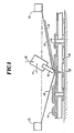
- a mesh screen is held between members 10 in a parallel position over the printed wiring board 11 resting on work surface 12 in order to superimpose on wiring traces 13 and initial photopolymer coating layer 19, a second layer 14, which is deposited from mesh screen 18 by means of the rubber blade 15 under influence of forces 16 and 17.
- an alternative intermediate step may be taken to provide a flush top surface upon which the phototool image pattern 20 is superimposed with the emulsion side in contact with the upper surface of the liquid photopolymer layer 14' .
- the upper layer 14' is partially polymerized to a depth of about .002 in. (.005 cm).
- the upper layer 14' is a liquid photopolymer layer having photo properties such that when a substantially constant thickness layer greater than about .002 in (.005 cm) thick has only one surface exposed to the presence of air and the other surface in contact with the phototransparency 20 carrying an image such as at 21 covering the through hole 22, that when subjected to actinic radiation in the order of .109 joules per square centimeter through the phototransparency, the liquid polymer layer will become polymerized to a depth of at least 30% of its thickness on the side adjacent the transparency and will be unpolymerized on the side exposed to air.
- the .003 in (.007cm) layer carried on the phototransparency 20 has two thirds of its thickness polymerized and one third remaining in liquid photopolymer unpolymerized form to provide when superimposed on a previously deposited liquid polymer layer surface to surface liquid photopolymer contact with the lower layer 1 9 of the liquid paste consistency photopolymer.
- This procedure insures that the wiring traces 13 will have solder mask coating at least .002 in (.005 cm) thick over all traces without starvation.
- a liquid photopolymer is a photosensitive polymer composition which does not contain volatiles, but only solids, where the photoactive polymers in the unpolymerized (unexposed by actinic radiation) state are in liquid or unhardened form.
- actinic radiation usually ultra violet radiation
- the photopolymer then becomes hardened in the polymerized state, such as over the particular pattern carried by the phototransparency image, so that the unpolymerized liquid photopolymer can be washed out in a development step.
- this invention provides a photopolymer solder mask layer for overlying fine, closely spaced wiring traces on a printed circuit board with a minimum depth of the solder mask covering thereover assured without starvation or thinning. Accordingly, the liquid solder mask polymer which has the character to be disposed on the printed wiring board in pastelike consistency to fill the gaps between the traces without air bubbles, even in undercut regions 23 alongside the wiring traces 13, and to form two superimposed layers in liquid to liquid surface interface, also assures thickness and quality of a solder mask overlying wiring traces.
- the method provided herein of depositing a substantially constant thickness layer of liquid photopolymer of the aforesaid-characteristics on the phototool transparency and exposing that layer to enough actinic radiation through the phototransparency with the outer photopolymer surface exposed to air to polymerize a substantial portion of the depth of the photopolymer layer adjacent the phototransparency while leaving the outer surface exposed to air in liquid unpolymerized form provides assurance of the thick solder mask coating over circuit board wiring traces upon which the photopolymer is transferred.
- This method dependent-upon special photopolymer characteristics, is characterized by the ability to preexpose the photopolymer layer on the phototransparency through the desired image with one surface exposed to air to permit polymerization through a part of the layer depth and a liquid opposite surface that has the property of conforming about wiring traces and other uneven surfaces, where the liquid part of the layer is then exposed through the phototransparency a second time to polymerize the coating through its entire depth and to secure the desired pattern of polymerized coating to the printed wiring board or other equivalent substrate, as a permanent coating.
- This is distinguished from known prior art preexposure techniques as set forth for example in U. S. Patent 4,087,182 H. Aiba et al. May, 1978, wherein preexposure required both surfaces of the liquid photopolymer to be covered, and was for the entirely different purpose and effect of preliminarily activating the photopolymerizable material so that the time required for exposure through the image could be shortened.
- the photosensitivity of the photopolymer which permits partial polymerisation of a layer when one side is exposed to air and the flow or viscosity characteristics giving a pastelike consistency to the liquid photopolymer are also critical So that it may be used directly on a printed wiring board over a specified area to cover wiring traces making the surface very uneven, the vicosity is in a restricted range. Also the viscosity is closely related to the thickness of the layer. Most of the commercially available liquid negative acting photopolymers thus have been specifically directed to very thin layers, such as a few microns.
- the flow characteristics are critical.
- the photopolymer need be capable of coating with a substantially constant thickness layer in the range of about .002 in (.005 cm) to about .004 in. (.01 cm). A simple and inexpensive way of doing this is by depositing from a mesh screen of a mesh between about 50 to 120.
- the general viscosity objective is to maintain a deposited layer in place with a viscosity thickness that in the deposited depth, it will not run off or change position at the edges to destroy a high resolution pattern when the board is handled; turned over, etc. Also it must be thin enough in viscosity to flow into and around circuit crevices between wiring traces, including undercuts, without entrapping air bubbles.
- the first as aforesaid is a partial exposure through the thickness of a liquid layer disposed on the phototransparency with one side of the layer exposed to the air during photo exposure through the phototransparency image to keep the air side in liquid form for flowing over and around the wiring traces.
- the second is with the transparency in place over the wiring traces and substrate where both surfaces are in air free contact for in depth exposure through the same phototransparency image to polymerize the entire thickness of the liquid polymer.
- This polymerization step cures the liquid layer through its entire depth over the same image pattern so that it may be developed by washing out the uncured liquid pohotopolymer but leaves the layer loosely bonded to the wiring board over the wiring traces.
- a defective layer need not to superimposed over the wiring.
- a defective solder mask layer it may be stripped from the board and a new mask laid down.
- a third curing and securing radiation exposure step may be made without an interposed phototransparency to expose the deposited pattern in place on the board after development, if inspection shows a properly deposited solder mask. If this final cure step is done at the second step, it would make board salvage difficult should there be a defect in the solder mask.
- the polymer thus need be of a characteristic not only to be partially polymerized through its thickness, as aforesaid, but also which permits a second step polymerization which cures through the entire depth of the layer but which does not so securely bind the layer to the wiring board that it may not be stripped.
- the photosensitivity is important in terms of energy applied to the photopolymer to polymerize it. Since it is desirable to use a flexible thin film transparency, the amount of heating in response to exposure radiation is very limited. Also standard and thus low cost radiation developing equipment using two mercury vapor lamps rated at 200 watts conveyance per linear inch is available. Thus the photosensitivity of the polymer need be matched to the capabilities of affordable processing equipment. In order to assure this, the photopolymer photo sensitivity is such that the results in the following examples may be attained. Since this invention is limited to a particular process with particular materials or specified dimensions. special tests in general are required to be meaningful. Thus the following conditions specify and define the unique combinational photo sensitivity properties necessary in the present invention.
- the photo sensitivity is such that with 30 second exposure to a one kilowatt mercury vapor lamp at a lamp to phototool distance of 30 in. (75 cm) a polymerized layer of .002 in. (.005 cm) thickness is formed next to the phototool and a layer .001 in. (.003 cm) thick regains unpolymerized on the surface exposed to air.
- the radiation energy thus received by the photopolymer is .109 Joules per square centimeter.
- the layer is polymerised through the depth and is bonded in place on the substrate.
- the radiation energy thus received by the photopolymer is 3.54 joules per square centimeter.
- the cure depth characteristic is alternatively measured as a cure depth of .024 in. (.06 cm) when conveyed at 10 feet (3.4 m) per minute past two tubular mercury vapor lamps, each rated at 200 watts per inch.
- the cure depth is satisfactory when there is no unpolymerized residue at .02 in. (.05 cm) depth.
- the desired photosensitivity level of a photopolymer may be established by the use of photosensiticers, such as those described in U. S. Patent 3,824, 104 H. A. Kloczewski, et al., July 16, 1974.
- photopolymer solder mask compositions afforded by and used in accordance with the teachings of this invention need to have ingredients compatibly interacting to provide the characteristics of high resolution (above about 100 lines) through layers of about. .002 in (.005 cm) to about .006 in. (.015 cm) with appropriate electrical insulation, together with adherance and thermal resistance properties when cured to produce a permanent solder mask coating on a printed wiring board.
- the viscosity and flow characteristics need to be such that wiring traces of up to .004 in (.01 cm) thickness may be covered without entrapment of air bubbles when transferred in a substantially constant thickness layer from screens with a mesh range of about 50 to 120.
- composition need have a photosensitivity characteristic such that energy and heat is low enough to work with thin polyester phototools and standard ultra violet lamp radiation sources, with polymerization and curing properties that are compatible with partial polymerization through a layer thickness, and two successive exposure cyles through a phototool image.
- a near 100% non volatile composition that does not change dimension significantly during processing and which in its liquid or unpolymerized (unexposed) form has a pastelike viscosity stably remaining in place where screened as a substantially constant thickness layer on a printed waring board for handling and inspection during Several manufacturing steps in converting the polymer in situ to a permanent high resolution solder mask coating pattern firmly secured to the wiring board over wiring traces theron.
- an easily applied test of the desired flow characteritics of the pastelike consistency photopolymers of this invention involves a test printed wiring board over which the liquid polymer is deposited.
- the viscosity and flow characteristics demanded by this invention are met if .004 in. (.01 cm) thick wiring traces .012 in. (.03 cm) wide, separated by .012 in. (.03 cm) spacings, are coated with the photopolymer from a 60 mesh polyester screen fabric and there are no mesh marks or air bubbles that remain on the surface and a uniform color is seen over the coating thereby indicating a substantially constant thickness coating over the rough surface.
- the photopolymer composition preferably includes a surfactant, or other wise controls bubble formation and surface tension, providing the characteristics of removing any mesh marks or bubbles from the screening step within a specified time period such as less than 30 seconds.
- a photoimaging quality solder mask negative acting photopolymer composition embodying the invention has the following consistency: All ingredients are shown as percentages by weight. An acceptable surfactant is available from Monsanto by the trade name "Modaflow”.
- This composition at an UV exposure of 0.6 joules per square cm. has a cure depth of 19.5 mils (.05 cm) with a tack free surface of pencil hardness 4H and resistance to methylene-chloride immersion greater than. ten minutes. This exposure is obtained by passing a coated specimen under three 200 watt per inch UV lamps at a rate of twelve feet per minute.
- the solder mask has the following set of properties:
- photopolymer solutions for use with 200 screen meshes and the like are conformed to desired viscosity by addition of fumed silica; were conformed where unacceptable to satisfactory depth of cure with one surface exposed to air by addition of up to 2 parts of photo-initiators such as Solex UV initiator UV 611 available from Advance Processing and Supply Corp.; were defoamed by addition of up to 0.1 part of BYK-052 defoamer, a surfactant available from BYK-Mallinekrodt Co., when surface bubbles did not dissipate after about ten seconds, and by adding up to 4 parts of hexanediol diacrylate.
- photo-initiators such as Solex UV initiator UV 611 available from Advance Processing and Supply Corp.
- BYK-052 defoamer a surfactant available from BYK-Mallinekrodt Co.
- Example 2 For any of those solutions of Example 2 that had photopolymer compositions with poor adhesion to copper surfaces, a dry B-stage epoxy powder that dossnot dissolve in the photopolymer composition but remains suspended, which becomes polymerized only after a threshold temperature. During the processing stage this serves as a filler which acts in attaining the hereinbefore specified.viscosity range. Typically 0.1 part is used.
- the copper to polymer bonding surface is generated by a final cure baking cycle at 275°F for 30 minutes. This liquifies the epoxy and bonds the epoxy sites to the copper surface forming a composite bonding structure reinforcing that of the polymer. Dielectric strength is also increased.
- a suitable such epoxy powder is available as Corvel ECA1555 from The Polymer Corp. of Reading, PA.
- the solution may include one of the available photo-initiators, preferably about 5% of that available from Ciba Geigg under the trademark "Ingacure #651".
Landscapes
- Physics & Mathematics (AREA)
- Engineering & Computer Science (AREA)
- General Physics & Mathematics (AREA)
- Manufacturing & Machinery (AREA)
- Microelectronics & Electronic Packaging (AREA)
- Mechanical Engineering (AREA)
- Spectroscopy & Molecular Physics (AREA)
- Non-Metallic Protective Coatings For Printed Circuits (AREA)
- Exposure And Positioning Against Photoresist Photosensitive Materials (AREA)
- Materials For Photolithography (AREA)
Applications Claiming Priority (2)
| Application Number | Priority Date | Filing Date | Title |
|---|---|---|---|
| US650109 | 1984-09-13 | ||
| US06/650,109 US4752553A (en) | 1982-04-01 | 1984-09-13 | High resolution solder mask photopolymers for screen coating over circuit traces |
Publications (2)
| Publication Number | Publication Date |
|---|---|
| EP0174555A2 true EP0174555A2 (fr) | 1986-03-19 |
| EP0174555A3 EP0174555A3 (fr) | 1987-08-19 |
Family
ID=24607499
Family Applications (1)
| Application Number | Title | Priority Date | Filing Date |
|---|---|---|---|
| EP85110855A Withdrawn EP0174555A3 (fr) | 1984-09-13 | 1985-08-28 | Photopolymères pour masque de soudure à haute résolution utilisés pour le recouvrement à l'écran de traces conductrices |
Country Status (6)
| Country | Link |
|---|---|
| US (1) | US4752553A (fr) |
| EP (1) | EP0174555A3 (fr) |
| JP (1) | JPS6187152A (fr) |
| KR (1) | KR860002739A (fr) |
| AU (3) | AU589908B2 (fr) |
| GB (1) | GB2164654B (fr) |
Cited By (3)
| Publication number | Priority date | Publication date | Assignee | Title |
|---|---|---|---|---|
| US7129109B2 (en) | 2001-02-02 | 2006-10-31 | Shell Solar Gmbh | Method for structuring an oxide layer applied to a substrate material |
| US7869844B2 (en) | 2004-09-15 | 2011-01-11 | Laird Technologies, Inc. | Sliding mechanism for opening and closing of cellular phone |
| US7967346B2 (en) | 2007-07-30 | 2011-06-28 | Laird Technologies Korea Yh | Slider mechanisms for opening and closing portable terminals |
Families Citing this family (11)
| Publication number | Priority date | Publication date | Assignee | Title |
|---|---|---|---|---|
| GB2241915A (en) * | 1990-03-17 | 1991-09-18 | Scapa Group Plc | Production of perforate structures. |
| US5667934A (en) * | 1990-10-09 | 1997-09-16 | International Business Machines Corporation | Thermally stable photoimaging composition |
| US5420171A (en) * | 1991-12-31 | 1995-05-30 | Tech Spray, Inc. | UV curable temporary solder mask |
| JP2856240B2 (ja) * | 1992-10-30 | 1999-02-10 | インターナショナル・ビジネス・マシーンズ・コーポレイション | プリント回路基板を再加工する方法 |
| US6611053B2 (en) * | 2000-06-08 | 2003-08-26 | Micron Technology, Inc. | Protective structure for bond wires |
| KR100442293B1 (ko) * | 2001-12-27 | 2004-07-30 | 엘지.필립스 엘시디 주식회사 | 패턴 형성방법 |
| EP2562599B1 (fr) | 2009-01-29 | 2014-12-10 | Digiflex Ltd. | Procédé de production d'un photomasque sur une surface photopolymérique |
| US20120097985A1 (en) * | 2010-10-21 | 2012-04-26 | Wen-Huang Liu | Light Emitting Diode (LED) Package And Method Of Fabrication |
| JP6955486B2 (ja) * | 2016-04-19 | 2021-10-27 | 株式会社カネカ | プリント配線板の製造方法 |
| EP3321330B1 (fr) * | 2016-11-10 | 2022-01-05 | Agfa-Gevaert Nv | Encres de jet d'encre de masque de soudure pour fabriquer des cartes de circuit imprimé |
| EP3901226A1 (fr) * | 2020-04-21 | 2021-10-27 | Agfa-Gevaert Nv | Procédé de fabrication d'une cartes de circuit imprimé |
Family Cites Families (31)
| Publication number | Priority date | Publication date | Assignee | Title |
|---|---|---|---|---|
| BE525225A (fr) * | 1951-08-20 | |||
| US3847767A (en) * | 1973-03-13 | 1974-11-12 | Grace W R & Co | Method of producing a screen printable photocurable solder resist |
| US3824104A (en) * | 1973-04-05 | 1974-07-16 | Grace W & Co Washington Res Ce | Solder resistant photopolymer composition |
| US4025348A (en) * | 1974-05-10 | 1977-05-24 | Hitachi Chemical Company, Ltd. | Photosensitive resin compositions |
| DE2443786C2 (de) * | 1974-09-13 | 1984-01-19 | Basf Ag, 6700 Ludwigshafen | Flüssige, photovernetzbare Formmasse zur Herstellung von Reliefdruckplatten |
| JPS51116703A (en) * | 1975-04-04 | 1976-10-14 | Asahi Chemical Ind | Method of producing photosensitive resin plate |
| DE2557408C2 (de) * | 1975-12-19 | 1983-08-25 | Bayer Ag, 5090 Leverkusen | Verfahren zur Herstellung eines in organischen Lösungsmitteln löslichen, vernetzbaren Acryloyl- und/oder Methacryloylgruppen und Carboxylgruppen enthaltenden Urethanharzes und seine Verwendung |
| SU941918A1 (ru) * | 1976-08-10 | 1982-07-07 | Предприятие П/Я Г-4444 | Сухой пленочный фоторезист |
| CA1116919A (fr) * | 1976-10-27 | 1982-01-26 | Joseph E. Gervay | Element retardateur de flammes, sensible au rayonnement, constitue d'une matiere photopolymerisable contenant des halogenes et un liant polymerique contenant de l'acrylonitrile |
| GB2030584B (en) * | 1978-10-03 | 1983-03-23 | Lankro Chem Ltd | Photopolymerisable solder resist compositions |
| US4510276A (en) * | 1979-12-13 | 1985-04-09 | Kollmorgen Technologies Corporation | Epoxy resin coating compositions for printed circuit boards |
| US4260675A (en) * | 1979-05-10 | 1981-04-07 | Sullivan Donald F | Photoprinting plate and method of preparing printed circuit board solder masks therewith |
| US4246147A (en) * | 1979-06-04 | 1981-01-20 | International Business Machines Corporation | Screenable and strippable solder mask and use thereof |
| BE883410A (fr) * | 1979-06-15 | 1980-11-21 | Du Pont | Film de photoresist pouvant etre developpe par un solvant |
| JPS5619752A (en) * | 1979-07-27 | 1981-02-24 | Hitachi Chemical Co Ltd | Photosensitive resin composition laminate |
| US4376815A (en) * | 1979-10-22 | 1983-03-15 | Oddi Michael J | Method of applying photoresist by screening in the formation of printed circuits |
| US4291118A (en) * | 1979-12-26 | 1981-09-22 | W. R. Grace & Co. | Relief imaging liquids |
| US4378411A (en) * | 1980-01-02 | 1983-03-29 | Minnesota Mining And Manufacturing Company | Radiation-curable polymers |
| US4424089A (en) * | 1980-05-08 | 1984-01-03 | Sullivan Donald F | Photoprinting process and apparatus for exposing paste-consistency photopolymers |
| US4506004A (en) * | 1982-04-01 | 1985-03-19 | Sullivan Donald F | Printed wiring board |
| JPS5711338A (en) * | 1980-06-23 | 1982-01-21 | Japan Synthetic Rubber Co Ltd | Film photoresist having laminate structure |
| DE3136818C2 (de) * | 1980-09-19 | 1990-08-02 | Hitachi Chemical Co., Ltd., Tokio/Tokyo | Verwendung eines lichtempfindlichen Gemisches und eines lichtempfindlichen Aufzeichnungsmaterials zur Bildung einer Lötmaske |
| JPS5764734A (en) * | 1980-10-08 | 1982-04-20 | Hitachi Chem Co Ltd | Photosensitive resin composition and photosensitive element |
| US4422914A (en) * | 1981-01-16 | 1983-12-27 | W. R. Grace & Co. | Polymer composition having terminal alkene and terminal carboxyl groups |
| US4438190A (en) * | 1981-03-04 | 1984-03-20 | Hitachi Chemical Company, Ltd. | Photosensitive resin composition containing unsaturated monomers and unsaturated phosphates |
| US4413051A (en) * | 1981-05-04 | 1983-11-01 | Dynamics Research Corporation | Method for providing high resolution, highly defined, thick film patterns |
| CA1198082A (fr) * | 1981-12-11 | 1985-12-17 | Gerald B. Fefferman | Enduction a distance des traversees d'une plaquette a circuit imprime, et durcissement de la sous-couche |
| GB2135326B (en) * | 1982-12-20 | 1986-09-03 | Fuji Photo Film Co Ltd | Photopolymerizable compositions having improved adhesive to metal surfaces |
| US4528261A (en) * | 1983-03-28 | 1985-07-09 | E. I. Du Pont De Nemours And Company | Prelamination, imagewise exposure of photohardenable layer in process for sensitizing, registering and exposing circuit boards |
| JPS59204036A (ja) * | 1983-05-06 | 1984-11-19 | Dainippon Ink & Chem Inc | レジストパタ−ンの形成法 |
| US4501689A (en) * | 1983-09-26 | 1985-02-26 | Makoto Yanagawa | Photopolymerizable composition |
-
1984
- 1984-09-13 US US06/650,109 patent/US4752553A/en not_active Expired - Fee Related
-
1985
- 1985-08-28 EP EP85110855A patent/EP0174555A3/fr not_active Withdrawn
- 1985-09-05 GB GB08522077A patent/GB2164654B/en not_active Expired
- 1985-09-06 AU AU47146/85A patent/AU589908B2/en not_active Ceased
- 1985-09-10 JP JP60200426A patent/JPS6187152A/ja active Pending
- 1985-09-12 KR KR1019850006673A patent/KR860002739A/ko not_active Withdrawn
-
1990
- 1990-01-10 AU AU47897/90A patent/AU4789790A/en not_active Abandoned
- 1990-01-10 AU AU47898/90A patent/AU4789890A/en not_active Abandoned
Cited By (3)
| Publication number | Priority date | Publication date | Assignee | Title |
|---|---|---|---|---|
| US7129109B2 (en) | 2001-02-02 | 2006-10-31 | Shell Solar Gmbh | Method for structuring an oxide layer applied to a substrate material |
| US7869844B2 (en) | 2004-09-15 | 2011-01-11 | Laird Technologies, Inc. | Sliding mechanism for opening and closing of cellular phone |
| US7967346B2 (en) | 2007-07-30 | 2011-06-28 | Laird Technologies Korea Yh | Slider mechanisms for opening and closing portable terminals |
Also Published As
| Publication number | Publication date |
|---|---|
| AU4789790A (en) | 1990-06-07 |
| US4752553A (en) | 1988-06-21 |
| GB8522077D0 (en) | 1985-10-09 |
| AU589908B2 (en) | 1989-10-26 |
| JPS6187152A (ja) | 1986-05-02 |
| AU4714685A (en) | 1986-03-20 |
| GB2164654A (en) | 1986-03-26 |
| EP0174555A3 (fr) | 1987-08-19 |
| KR860002739A (ko) | 1986-04-28 |
| GB2164654B (en) | 1988-07-06 |
| AU4789890A (en) | 1990-06-07 |
Similar Documents
| Publication | Publication Date | Title |
|---|---|---|
| US4752553A (en) | High resolution solder mask photopolymers for screen coating over circuit traces | |
| US4424089A (en) | Photoprinting process and apparatus for exposing paste-consistency photopolymers | |
| CA1208811A (fr) | Exposition d'une couche photodurcissable a une image dans un processus d'activation de cartes de circuits | |
| US4260675A (en) | Photoprinting plate and method of preparing printed circuit board solder masks therewith | |
| CA1131791A (fr) | Utilisation d'un support photosensible pour produire des connexions a trou passant dans les plaques a circuits imprimes | |
| US4506004A (en) | Printed wiring board | |
| EP0141868A1 (fr) | Ensemble photomasque à haut pouvoir résolvant pour l'obtention d'images avec des photopolymères | |
| US4291116A (en) | Method of image reproduction and materials therefor | |
| US4631111A (en) | Dichromic process for preparation of conductive circuit | |
| JPH0756355A (ja) | 回路板の被覆方法 | |
| US4645733A (en) | High resolution printed circuits formed in photopolymer pattern indentations overlaying printed wiring board substrates | |
| US4888270A (en) | Photoprinting process and apparatus for exposing paste consistency photopolymers | |
| US4954421A (en) | Photoflashing a liquid polymer layer on a phototool surface exposed to air | |
| EP0096863B1 (fr) | Procédé pour le positionnement et l'insolation de feuilles portant un liquide photosensible | |
| JPH02135349A (ja) | 光撮像可能な永久レジスト | |
| CN107443947A (zh) | 网版图案及其制造方法 | |
| US4657839A (en) | Photoprinting process and apparatus for exposing paste-consistency photopolymers | |
| US4669869A (en) | Photoprinting process and apparatus for exposing paste-consistency photopolymers | |
| EP0150623A2 (fr) | Matériel photosensible pour stencil | |
| US4560639A (en) | Reusable phototransparency image forming tools for direct contact printing | |
| US4618567A (en) | High resolution liquid photopolymer coating patterns over irregular printed wiring board surface conductors | |
| CA1197406A (fr) | Transfert d'images haute resolution par phototransparence a l'aide de photopolymeres | |
| DE2845754A1 (de) | Bildreproduktionsverfahren und materialien dafuer | |
| GB2166253A (en) | Printed circuit boards | |
| GB2151365A (en) | High resolution image forming with photopolymers |
Legal Events
| Date | Code | Title | Description |
|---|---|---|---|
| PUAI | Public reference made under article 153(3) epc to a published international application that has entered the european phase |
Free format text: ORIGINAL CODE: 0009012 |
|
| AK | Designated contracting states |
Kind code of ref document: A2 Designated state(s): BE DE FR IT NL SE |
|
| PUAL | Search report despatched |
Free format text: ORIGINAL CODE: 0009013 |
|
| AK | Designated contracting states |
Kind code of ref document: A3 Designated state(s): BE DE FR IT NL SE |
|
| 17P | Request for examination filed |
Effective date: 19871113 |
|
| RAP1 | Party data changed (applicant data changed or rights of an application transferred) |
Owner name: M&T CHEMICALS INC. |
|
| RIN1 | Information on inventor provided before grant (corrected) | ||
| RIN1 | Information on inventor provided before grant (corrected) |
Inventor name: SULLIVAN, DONALD FORT |
|
| 17Q | First examination report despatched |
Effective date: 19900126 |
|
| STAA | Information on the status of an ep patent application or granted ep patent |
Free format text: STATUS: THE APPLICATION IS DEEMED TO BE WITHDRAWN |
|
| 18D | Application deemed to be withdrawn |
Effective date: 19900806 |
|
| RIN1 | Information on inventor provided before grant (corrected) |
Inventor name: SULLIVAN, DONALD FORT |