EP0174638A2 - Circuit intégré avec fonction de contrôle d'un signal interne - Google Patents
Circuit intégré avec fonction de contrôle d'un signal interne Download PDFInfo
- Publication number
- EP0174638A2 EP0174638A2 EP85111433A EP85111433A EP0174638A2 EP 0174638 A2 EP0174638 A2 EP 0174638A2 EP 85111433 A EP85111433 A EP 85111433A EP 85111433 A EP85111433 A EP 85111433A EP 0174638 A2 EP0174638 A2 EP 0174638A2
- Authority
- EP
- European Patent Office
- Prior art keywords
- signal
- integrated circuit
- refresh
- internal
- voltage
- Prior art date
- Legal status (The legal status is an assumption and is not a legal conclusion. Google has not performed a legal analysis and makes no representation as to the accuracy of the status listed.)
- Granted
Links
Images

Classifications
-
- G—PHYSICS
- G11—INFORMATION STORAGE
- G11C—STATIC STORES
- G11C7/00—Arrangements for writing information into, or reading information out from, a digital store
- G11C7/22—Read-write [R-W] timing or clocking circuits; Read-write [R-W] control signal generators or management
-
- G—PHYSICS
- G11—INFORMATION STORAGE
- G11C—STATIC STORES
- G11C11/00—Digital stores characterised by the use of particular electric or magnetic storage elements; Storage elements therefor
- G11C11/21—Digital stores characterised by the use of particular electric or magnetic storage elements; Storage elements therefor using electric elements
- G11C11/34—Digital stores characterised by the use of particular electric or magnetic storage elements; Storage elements therefor using electric elements using semiconductor devices
- G11C11/40—Digital stores characterised by the use of particular electric or magnetic storage elements; Storage elements therefor using electric elements using semiconductor devices using transistors
- G11C11/401—Digital stores characterised by the use of particular electric or magnetic storage elements; Storage elements therefor using electric elements using semiconductor devices using transistors forming cells needing refreshing or charge regeneration, i.e. dynamic cells
- G11C11/406—Management or control of the refreshing or charge-regeneration cycles
Definitions
- the present invention relates to integrated circuits and more particularly to integrated circuit memory devices having automatic refreshing function.
- Integrated circuits have been widely used in various fields, and types of integrated circuits are very large in number.
- the above type IC memory has a refresh timer circuit and an auto-refresh timing signal generator.
- a refresh control signal applied to the refresh timer circuit from the outside is kept at an active level
- the refresh timer circuit produces an internal refresh command signal intermittently
- the auto-refresh timing signal generator produces a refresh timing signal for allowing an internal refresh operation in response to the internal command signal.
- refresh control signal is kept active, refresh of memory cells is sequentially conducted without necessity of control from the outside.
- a long period of time has been required to evaluate data-holding function of memory cells in such memory because a holding time of memory cells is generally 10 seconds or more and generally two to three times of the holding time is employed in evaluation in order to take the safety side.
- evaluation of memories would be conducted effectively.
- the number of pins of such memories has been limited to a certain number, e.g. 16, according to the commercial specification or standard, and therefore there has been no allowance to provide an additonal pin for observing the internal signal.
- the integrated circuit according to the invention is of the type having a semiconductor chip, first and second functional circuits formed on the chip, the first functional circuit generating an internal signal in response to at least one input signal, the second functional circuit receiving the internal signal and generating an output to be driven outside the chip, and is featured in that a detection circuit for detecting the internal signal is provided on the chip.
- the detection circuit includes a transistor adapted to receive the internal signal at a control electrode, and a voltage switching element which assumes a conductive state when a voltage of a predetermined value or more is impressed thereacross.
- the transistor and the voltage switching elements are connected in series between two of external terminals.
- the voltage switching element By applying a voltage of the predetermined value or more between the above two terminals, the voltage switching element is rendered conductive, so that a current corresponding to the internal signal flows through the series connection of the transistor and the voltage switching element. Thus, the state of the internal signal can be detected by observing the current flowing through the series connection.
- a dynamic memory to which the present invention is applied is described.
- the memory device formed on a semiconductor chip 1 includes a memory cell matrix 101 of dynamic type memory cells arranged in rows and columns, a circuit block 102 of sense amplifiers and data I/O gates.
- the memory is known multi-addressing type in which row address signals and column address signals are taken in via set of address input terminals A 1 to An in response to active levels of a row address strobe RAS and a column address strobe CAS, respectively.
- a RAS input buffer control logic circuit 114 receives RAS and drives a RAS clock generator 115 which generates a timing signal ⁇ L for enabling a row address inverter buffer 118, a timing signal ⁇ D for enabling a row decoder 116 to select one of rows of the matrix 101 and a timing signal ⁇ D for enabling sense amplifiers to refresh contents of the memory cells on the selected row.
- a CAS clock generator 108 receives CAS and the timing signal ⁇ R and generates a timing signal ⁇ C for enabling a column address inverter buffer 104, a column decoder 103, data I/O gates, a write clock generator 107, a data input buffer 106 and a data output buffer 105, in a known predetermined sequence.
- the signal ⁇ C is representatively illustrated as a single timing signal, a plurality of sequential signals are employed for the above blocks 104, 103, 107, 106 and 105 in practice case.
- the memory is provided with a refresh control timer 109, an auto refreshing timing generator 112, a refresh address counter 113 and a multiplexer 117.
- the refresh timer 109 receives a refresh control signal RFSH , and generates control signals R 1 to R 3 when RFSH is kept at a low level, thereby to introduce an internal refresh mode to the memory.
- control signal R 1 controls the multiplexer 117 so that the multiplexer connects parallel outputs RC of the address counter 113 to the row decoder 116 in place of the output of the row address inverter buffer 118.
- the control signal R 2 enables the auto refresh timing generator 112 so that the generator 112 produces a refresh timing signal ⁇ Ra at the beginning of each refresh cycle which is applied to the RAS input buffer control logic circuit 114 and a refresh address incrementing signal ⁇ Rb which is applied to the refresh address counter 113 thereby to increment the content of the counter 113.
- the circuit 114 controls the RAS clock generator 115 so that the generator 115 generates the timing signals ⁇ L , ⁇ D and ⁇ R .
- the row decoder 116 selects one of rows of the matrix 101 based on the content of the refresh address counter 113 and the sense amplifiers 102 are enabled in response to the timing signal 0 R thereby to refresh the memory cells on the selected row. Thereafter, the address content of the address counter 113 in response to the signal ⁇ Rb .
- the above sequence of operations are repeated as long as the RFSH is kept at a low level.
- the further detailed feature of this memory is disclosed in United States Patent Specification No. 4,334,295 issued to Nagami.
- a refresh detecting circuit 10 is provided on the semiconductor chip 1 according to the present invention.
- the refresh detection circuit 10 includes a field effect transistor Q 12 having a gate receiving the signal ⁇ R and a source coupled to a power voltage terminal V CC and a field effect transistor Q 11 having a gate and a drain commonly connected to a write control terminal WE which assumes a high level during a read cycle and a refresh cycle and a low level during a write cycle, and a source connected to a drain of the transistor Q 12 .
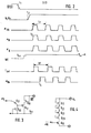
- RFSH is turned to a low (GND) level from a high level at a time point t 1 , and the refresh time 109 generates the signals R 1 and R 2 at a time point t 2 so that an internal refresh mode is introduced in the memory.
- the timing generator 112 generates the signal ⁇ Ra at a time point t 3 so that the RAS clock generator 115 generates the signals ⁇ D and ⁇ R so that the output RC of the refresh address counter 113 drives the row decoder 116 so as to select one row of the matrix and contents of memory cells on the selected row are refreshed by the sense amplifiers.
- the terminal WE is raised to the voltage (V CC + ⁇ ) which is larger than the sum of the voltage V CC and a threshold voltage of the transistor Q 11 , from t 2 .
- the memory does not operate in a write cycle, there is affection on a write clock generator 107.
- the transistor Q 11 assumes a conductive state so that a detection current Idet flows from the terminal WE to the voltage terminal in response to the activation of the signal ⁇ R substantially at t 3 .
- the timing generator 112 After the refresh conducted by the signal ⁇ R , the timing generator 112 generates the signal ⁇ Rb to increment the content of the refresh address counter 112 for preparation of a subsequent refresh cycle, at a time point t 4 .
- the timing generator 112 After a refresh cycle period T F has elapsed from t 3 , the timing generator 112 generates the signal ⁇ RA and the clock generator 115 generates the signals ⁇ D and ⁇ R , so that memory cells on the different row are refreshed.
- the above refresh cycle is repeatedly with a refresh cycle T F which is solely determined by the timing generator 112 and cannot be controlled from the outside. As illustrated, the above refresh cycle T F can be observed by the current Idet flowing through the terminal WE according to the invention.
- the signal ⁇ D or ⁇ Ra may be applied to the gate of the transistor Q 12 .
- the gate and drain of the transistor Q 11 may be connected to other terminal which is not used in the refresh cycle.
- Fig. 3. shows another embodiment of the refresh detecting circuit 10.
- a field effect transistor Q 13 and a boot capacitor C 21 are further provided to the circuit 10 of Fig. 1. Namely, a drain-source path of the transistor Q 13 is coupled between the power voltage terminal V CC and the gate of the transistor Q 12 with a gate coupled to V CC .
- the internal signal ⁇ R is applied to the gate of the transistor Q 12 via the capacitor C 21 .
- the gate of Q 22 is at a potential of (V CC - V TH ) in which V TH is a the threshold voltage of the transistor Q 12 . Therefore, Q 12 assumes a non-conductive state.
- Fig. 4 shows a third embodiment of the invention.
- diode-connected field effect transistors Q 21 to Q 23 are inserted in series between the source of the transistor Q 11 and the drain of the transistor Q12.
- two address input terminals A. and A. are connected to the transistors Q 11 and Q12.
- a detection of the internal signal ⁇ R is performed.
- the detection of an internal signal is conducted effectively according to the invention. It should be noted that the present invention is not limited to the above embodiment. For example, the present invention applicable to integrated circuits other than memories.
Landscapes
- Engineering & Computer Science (AREA)
- Microelectronics & Electronic Packaging (AREA)
- Computer Hardware Design (AREA)
- Dram (AREA)
- For Increasing The Reliability Of Semiconductor Memories (AREA)
Applications Claiming Priority (2)
| Application Number | Priority Date | Filing Date | Title |
|---|---|---|---|
| JP189107/84 | 1984-09-10 | ||
| JP59189107A JPS6166295A (ja) | 1984-09-10 | 1984-09-10 | 半導体メモリ |
Publications (3)
| Publication Number | Publication Date |
|---|---|
| EP0174638A2 true EP0174638A2 (fr) | 1986-03-19 |
| EP0174638A3 EP0174638A3 (en) | 1989-09-13 |
| EP0174638B1 EP0174638B1 (fr) | 1992-04-01 |
Family
ID=16235481
Family Applications (1)
| Application Number | Title | Priority Date | Filing Date |
|---|---|---|---|
| EP85111433A Expired EP0174638B1 (fr) | 1984-09-10 | 1985-09-10 | Circuit intégré avec fonction de contrôle d'un signal interne |
Country Status (4)
| Country | Link |
|---|---|
| US (1) | US4807197A (fr) |
| EP (1) | EP0174638B1 (fr) |
| JP (1) | JPS6166295A (fr) |
| DE (1) | DE3585760D1 (fr) |
Cited By (3)
| Publication number | Priority date | Publication date | Assignee | Title |
|---|---|---|---|---|
| EP0239916A3 (en) * | 1986-03-24 | 1989-06-14 | Nec Corporation | Refresh address counter test control circuit for dynamic random access memory system |
| EP0519584A3 (en) * | 1991-06-21 | 1993-09-22 | Sharp Kabushiki Kaisha | Semiconductor memory |
| US5347491A (en) * | 1991-04-11 | 1994-09-13 | Nec Corporation | Dynamic random access memory device having autorefreshing unit for producing internal row address strobe signal and internal column address strobe signal |
Families Citing this family (3)
| Publication number | Priority date | Publication date | Assignee | Title |
|---|---|---|---|---|
| KR100372245B1 (ko) * | 1995-08-24 | 2004-02-25 | 삼성전자주식회사 | 워드라인순차제어반도체메모리장치 |
| US6075744A (en) * | 1997-10-10 | 2000-06-13 | Rambus Inc. | Dram core refresh with reduced spike current |
| DE102006020098A1 (de) * | 2006-04-29 | 2007-10-31 | Infineon Technologies Ag | Speicherschaltung und Verfahren zum Auffrischen von dynamischen Speicherzellen |
Family Cites Families (5)
| Publication number | Priority date | Publication date | Assignee | Title |
|---|---|---|---|---|
| US4145760A (en) * | 1978-04-11 | 1979-03-20 | Ncr Corporation | Memory device having a reduced number of pins |
| JPS55150192A (en) * | 1979-05-08 | 1980-11-21 | Nec Corp | Memory unit |
| JPS5835783A (ja) * | 1981-08-24 | 1983-03-02 | Fujitsu Ltd | 半導体メモリ |
| JPS5972153A (ja) * | 1982-10-18 | 1984-04-24 | Toshiba Corp | 半導体集積回路装置 |
| JPS59104795A (ja) * | 1982-12-06 | 1984-06-16 | Mitsubishi Electric Corp | 半導体メモリ装置 |
-
1984
- 1984-09-10 JP JP59189107A patent/JPS6166295A/ja active Granted
-
1985
- 1985-09-10 DE DE8585111433T patent/DE3585760D1/de not_active Expired - Lifetime
- 1985-09-10 US US06/774,430 patent/US4807197A/en not_active Expired - Fee Related
- 1985-09-10 EP EP85111433A patent/EP0174638B1/fr not_active Expired
Cited By (3)
| Publication number | Priority date | Publication date | Assignee | Title |
|---|---|---|---|---|
| EP0239916A3 (en) * | 1986-03-24 | 1989-06-14 | Nec Corporation | Refresh address counter test control circuit for dynamic random access memory system |
| US5347491A (en) * | 1991-04-11 | 1994-09-13 | Nec Corporation | Dynamic random access memory device having autorefreshing unit for producing internal row address strobe signal and internal column address strobe signal |
| EP0519584A3 (en) * | 1991-06-21 | 1993-09-22 | Sharp Kabushiki Kaisha | Semiconductor memory |
Also Published As
| Publication number | Publication date |
|---|---|
| JPH048876B2 (fr) | 1992-02-18 |
| US4807197A (en) | 1989-02-21 |
| DE3585760D1 (de) | 1992-05-07 |
| JPS6166295A (ja) | 1986-04-05 |
| EP0174638A3 (en) | 1989-09-13 |
| EP0174638B1 (fr) | 1992-04-01 |
Similar Documents
| Publication | Publication Date | Title |
|---|---|---|
| US4612630A (en) | EEPROM margin testing design | |
| KR100196977B1 (ko) | 프로그래머블 다이나믹 랜덤 액세스 메모리 | |
| US4821238A (en) | Semiconductor memory device having test pattern generating circuit | |
| EP0128499B1 (fr) | Mémoire MOS | |
| US5204837A (en) | Semiconductor memory device having test mode | |
| US5365481A (en) | Semiconductor memory device having test mode and method of setting test mode | |
| KR100203529B1 (ko) | 다이나믹형 반도체메모리 및 그 테스트방법 | |
| CA1048645A (fr) | Methode d'essai pour memoire a semiconducteurs | |
| KR960001327B1 (ko) | 테스트모드기능 내장 다이내믹 랜덤 액세스 메모리장치 | |
| US5265057A (en) | Semiconductor memory | |
| EP0509360B1 (fr) | Dispositif de mémoire à accès sélectif muni d'un sélecteur à multiple ligne des mots usé dans un test de marquage à chaud | |
| JPH0346193A (ja) | スタティック型半導体記憶装置 | |
| EP0585870A2 (fr) | Mémoire dynamique à accès aléatoire comportant un circuit d'application de tension élevée | |
| US5414672A (en) | Semiconductor memory device including address transition detector | |
| US4725985A (en) | Circuit for applying a voltage to a memory cell MOS capacitor of a semiconductor memory device | |
| US4742486A (en) | Semiconductor integrated circuit having function for switching operational mode of internal circuit | |
| US6327198B1 (en) | Semiconductor memory device having a test mode setting circuit | |
| US5432744A (en) | Dynamic semiconductor memory circuit | |
| US5608674A (en) | Semiconductor memory device | |
| US4802134A (en) | Semiconductor memory device having serial addressing scheme | |
| EP0174638A2 (fr) | Circuit intégré avec fonction de contrôle d'un signal interne | |
| US4760559A (en) | Semiconductor memory device | |
| EP0456255B1 (fr) | Dispositif de mémoire dynamique et méthode pour l'examiner | |
| KR100191023B1 (ko) | 외부 입출력제어신호에 대한 입력버퍼회로의 관통전류를 제어 할 수 있는 다이나믹형 반도체 기억장치 | |
| US5949724A (en) | Burn-in stress circuit for semiconductor memory device |
Legal Events
| Date | Code | Title | Description |
|---|---|---|---|
| PUAI | Public reference made under article 153(3) epc to a published international application that has entered the european phase |
Free format text: ORIGINAL CODE: 0009012 |
|
| 17P | Request for examination filed |
Effective date: 19850910 |
|
| AK | Designated contracting states |
Kind code of ref document: A2 Designated state(s): DE FR GB |
|
| PUAL | Search report despatched |
Free format text: ORIGINAL CODE: 0009013 |
|
| AK | Designated contracting states |
Kind code of ref document: A3 Designated state(s): DE FR GB |
|
| 17Q | First examination report despatched |
Effective date: 19901005 |
|
| GRAA | (expected) grant |
Free format text: ORIGINAL CODE: 0009210 |
|
| AK | Designated contracting states |
Kind code of ref document: B1 Designated state(s): DE FR GB |
|
| REF | Corresponds to: |
Ref document number: 3585760 Country of ref document: DE Date of ref document: 19920507 |
|
| ET | Fr: translation filed | ||
| PLBE | No opposition filed within time limit |
Free format text: ORIGINAL CODE: 0009261 |
|
| STAA | Information on the status of an ep patent application or granted ep patent |
Free format text: STATUS: NO OPPOSITION FILED WITHIN TIME LIMIT |
|
| 26N | No opposition filed | ||
| PGFP | Annual fee paid to national office [announced via postgrant information from national office to epo] |
Ref country code: DE Payment date: 19931123 Year of fee payment: 9 |
|
| PGFP | Annual fee paid to national office [announced via postgrant information from national office to epo] |
Ref country code: GB Payment date: 19940908 Year of fee payment: 10 |
|
| PGFP | Annual fee paid to national office [announced via postgrant information from national office to epo] |
Ref country code: FR Payment date: 19940916 Year of fee payment: 10 |
|
| PG25 | Lapsed in a contracting state [announced via postgrant information from national office to epo] |
Ref country code: DE Effective date: 19950601 |
|
| PG25 | Lapsed in a contracting state [announced via postgrant information from national office to epo] |
Ref country code: GB Effective date: 19950910 |
|
| GBPC | Gb: european patent ceased through non-payment of renewal fee |
Effective date: 19950910 |
|
| PG25 | Lapsed in a contracting state [announced via postgrant information from national office to epo] |
Ref country code: FR Effective date: 19960531 |
|
| REG | Reference to a national code |
Ref country code: FR Ref legal event code: ST |