EP0174773A2 - Dispositif semi-conducteur avec couches d'interconnexion - Google Patents
Dispositif semi-conducteur avec couches d'interconnexion Download PDFInfo
- Publication number
- EP0174773A2 EP0174773A2 EP85306106A EP85306106A EP0174773A2 EP 0174773 A2 EP0174773 A2 EP 0174773A2 EP 85306106 A EP85306106 A EP 85306106A EP 85306106 A EP85306106 A EP 85306106A EP 0174773 A2 EP0174773 A2 EP 0174773A2
- Authority
- EP
- European Patent Office
- Prior art keywords
- semiconductor device
- metallic silicide
- region
- aluminium
- nitrided
- Prior art date
- Legal status (The legal status is an assumption and is not a legal conclusion. Google has not performed a legal analysis and makes no representation as to the accuracy of the status listed.)
- Granted
Links
Images
Classifications
-
- H—ELECTRICITY
- H10—SEMICONDUCTOR DEVICES; ELECTRIC SOLID-STATE DEVICES NOT OTHERWISE PROVIDED FOR
- H10W—GENERIC PACKAGES, INTERCONNECTIONS, CONNECTORS OR OTHER CONSTRUCTIONAL DETAILS OF DEVICES COVERED BY CLASS H10
- H10W20/00—Interconnections in chips, wafers or substrates
- H10W20/01—Manufacture or treatment
- H10W20/031—Manufacture or treatment of conductive parts of the interconnections
- H10W20/064—Manufacture or treatment of conductive parts of the interconnections by modifying the conductivity of conductive parts, e.g. by alloying
- H10W20/066—Manufacture or treatment of conductive parts of the interconnections by modifying the conductivity of conductive parts, e.g. by alloying by forming silicides of refractory metals
-
- H—ELECTRICITY
- H10—SEMICONDUCTOR DEVICES; ELECTRIC SOLID-STATE DEVICES NOT OTHERWISE PROVIDED FOR
- H10W—GENERIC PACKAGES, INTERCONNECTIONS, CONNECTORS OR OTHER CONSTRUCTIONAL DETAILS OF DEVICES COVERED BY CLASS H10
- H10W20/00—Interconnections in chips, wafers or substrates
- H10W20/40—Interconnections external to wafers or substrates, e.g. back-end-of-line [BEOL] metallisations or vias connecting to gate electrodes
- H10W20/41—Interconnections external to wafers or substrates, e.g. back-end-of-line [BEOL] metallisations or vias connecting to gate electrodes characterised by their conductive parts
- H10W20/44—Conductive materials thereof
- H10W20/4403—Conductive materials thereof based on metals, e.g. alloys, metal silicides
- H10W20/4437—Conductive materials thereof based on metals, e.g. alloys, metal silicides the principal metal being a transition metal
- H10W20/4441—Conductive materials thereof based on metals, e.g. alloys, metal silicides the principal metal being a transition metal the principal metal being a refractory metal
-
- Y—GENERAL TAGGING OF NEW TECHNOLOGICAL DEVELOPMENTS; GENERAL TAGGING OF CROSS-SECTIONAL TECHNOLOGIES SPANNING OVER SEVERAL SECTIONS OF THE IPC; TECHNICAL SUBJECTS COVERED BY FORMER USPC CROSS-REFERENCE ART COLLECTIONS [XRACs] AND DIGESTS
- Y10—TECHNICAL SUBJECTS COVERED BY FORMER USPC
- Y10S—TECHNICAL SUBJECTS COVERED BY FORMER USPC CROSS-REFERENCE ART COLLECTIONS [XRACs] AND DIGESTS
- Y10S148/00—Metal treatment
- Y10S148/019—Contacts of silicides
Definitions
- This invention relates to semiconductor devices and the manufacture thereof and, in particular, to semiconductor devices including silicides.
- Polysilicon has conventionally been employed for gates and interconnections in integrated circuits. However, for small geometry, high speed integrated circuits it is desirable to use alternative materials with lower resistivity, such as metallic silicides.
- Our co-pending GB Applications No.8328552 Serial No.
- No.8312281 Serial No.2139419 (P.D. Scovell et al 7-4-3) describe methods of forming metallic silicide elements.
- Titanium disilicide is now one of the most favoured replacements for heavily-doped polysilicon as an interconnect in MOS devices with geometries down to lum. Titanium disilicide has numerous beneficial qualities. It is a refractory metal. It has the lowest thin film resistivity of any refractory silicide. It is readily etched. Metal over the silicide can be etched with great selectivity, and a high quality silicon dioxide layer can be grown over the silicide with no chance of forming volatile metal oxides. One significant disadvantage of this material is that it does not form a barrier to silicon diffusion from beneath the silicide. Thus where aluminium is disposed over silicide, silicon can diffuse up into the aluminium where it can precipitate to form a high resistance layer, and this diffusion is a significant cause of device failure.
- a semiconductor device characterised by a metallic silicide element (1) and a metal element (6) in electrical contact therewith via a nitrided region (5)-of the metallic silicide element (1).
- a method of manufacturing a semiconductor device characterised by the steps of forming a metallic silicide element (1) on a semiconductor wafer (2), providing an electrically insulating layer (3) over the wafer, exposing a region of the metallic silicide element (1) via a hole in the electrically insulating layer (3), annealing the wafer in nitrogen whereby to locally nitride (5) the exposed metallic silicide region (1), metallising the wafer, and patterning the metallisation to form a metal element (6), the metallic silicide element (1) being in electrical contact with the metal element (6) via the locally nitrided metallic silicide region (5).
- a method of manufacturing a semiconductor device characterised by the steps of forming a titanium disilicide interconnect (1), locally nitriding a region (5) of the interconnect (1) and disposing an aluminium element (6) in electrical contact with the nitrided region (5).
- Titanium nitride is known to be a good barrier to silicon diffusion while still having an acceptably low resistivity. It is thus proposed to selectively form titanium nitride at points where electrical contact between aluminium metallisation and underlying titanium silicide is required.
- the silicide provides a low resistivity interconnect while the nitride provides the ideal contact material to aluminium, having a low contact resistance and preventing silicon diffusing up into the aluminium.
- the titanium nitride can be formed in a simple manner with only minimal disturbance to the conventional MOS Process.
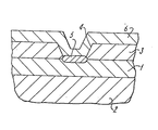
- reference numeral 1 indicates a titanium disilicide interconnect extending over a substrate 2 (wafer) including active components (not shown) of an integrated circuit.
- Such an interconnect 1 is manufactured by forming a layer of titanium disilicide over the substrate 2 and subsequent patterning thereof. After patterning the silicide, a thick oxide (silicon dioxide) layer 3 is provided over the entire wafer. Holes such as 4 are then cut (etched) in layer 3 to expose the silicide 1.
- the processing steps outlined above are those of the normal MOS Process.
- the next step which is not part of the normal MOS Process, comprises annealing the wafer in nitrogen. The nitrogen reacts with silicide exposed by the holes 4 to form titanium nitride regions (contacts) 5 thereat. The only exposed silicide is in the contact holes 4. Following this anneal, aluminium is deposited as in the normal MOS process, resulting in layer 5 which can be subsequently patterned as in the normal process.
- the annealing in nitrogen may involve, for example, a temperature of 1000°C for one hour, or alternatively 1100°C for a few seconds. Both processes result in the formation of an adequate titanium nitride region 5.
- the method proposed thus involves locally nitriding a low resistivity silicide interconnect to form a low resistivity nitride region which forms a barrier to silicon diffusion.
- the process used to form the nitride layer is simple and achieves a truly self-aligned barrier.
Landscapes
- Internal Circuitry In Semiconductor Integrated Circuit Devices (AREA)
- Electrodes Of Semiconductors (AREA)
- Bipolar Transistors (AREA)
- Heterocyclic Carbon Compounds Containing A Hetero Ring Having Oxygen Or Sulfur (AREA)
- Recrystallisation Techniques (AREA)
- Semiconductor Integrated Circuits (AREA)
- Semiconductor Memories (AREA)
Priority Applications (1)
| Application Number | Priority Date | Filing Date | Title |
|---|---|---|---|
| AT85306106T ATE60853T1 (de) | 1984-09-14 | 1985-08-29 | Halbleiteranordnung mit verbindungsschichten. |
Applications Claiming Priority (2)
| Application Number | Priority Date | Filing Date | Title |
|---|---|---|---|
| GB08423265A GB2164491B (en) | 1984-09-14 | 1984-09-14 | Semiconductor devices |
| GB8423265 | 1984-09-14 |
Publications (3)
| Publication Number | Publication Date |
|---|---|
| EP0174773A2 true EP0174773A2 (fr) | 1986-03-19 |
| EP0174773A3 EP0174773A3 (en) | 1987-01-21 |
| EP0174773B1 EP0174773B1 (fr) | 1991-02-06 |
Family
ID=10566719
Family Applications (1)
| Application Number | Title | Priority Date | Filing Date |
|---|---|---|---|
| EP85306106A Expired - Lifetime EP0174773B1 (fr) | 1984-09-14 | 1985-08-29 | Dispositif semi-conducteur avec couches d'interconnexion |
Country Status (6)
| Country | Link |
|---|---|
| US (1) | US4772571A (fr) |
| EP (1) | EP0174773B1 (fr) |
| JP (1) | JPS6173370A (fr) |
| AT (1) | ATE60853T1 (fr) |
| DE (1) | DE3581682D1 (fr) |
| GB (1) | GB2164491B (fr) |
Cited By (5)
| Publication number | Priority date | Publication date | Assignee | Title |
|---|---|---|---|---|
| EP0194950A3 (en) * | 1985-03-15 | 1988-08-10 | Fairchild Semiconductor Corporation | High temperature interconnect system for an integrated circuit |
| EP0363133A1 (fr) * | 1988-10-06 | 1990-04-11 | The Boc Group, Inc. | Procédé de métallisation d'un circuit intégré |
| US4920071A (en) * | 1985-03-15 | 1990-04-24 | Fairchild Camera And Instrument Corporation | High temperature interconnect system for an integrated circuit |
| DE4228679A1 (de) * | 1991-08-30 | 1993-03-11 | Mitsubishi Electric Corp | Kontaktstruktur und verfahren zu deren herstellung sowie halbleiterspeichereinrichtung und verfahren zu deren herstellung |
| KR200465941Y1 (ko) * | 2011-11-11 | 2013-03-19 | 박혜원 | 쿠션 쇼파 |
Families Citing this family (37)
| Publication number | Priority date | Publication date | Assignee | Title |
|---|---|---|---|---|
| US4931411A (en) * | 1985-05-01 | 1990-06-05 | Texas Instruments Incorporated | Integrated circuit process with TiN-gate transistor |
| JPS6358927A (ja) * | 1986-08-29 | 1988-03-14 | Mitsubishi Electric Corp | 半導体装置の製造方法 |
| CA1306072C (fr) * | 1987-03-30 | 1992-08-04 | John E. Cronin | Structures conductrices composees d'un metal refractaire et d'une mince couche de nitrure de titanium, et procedes de fabrication connexes |
| US4962414A (en) * | 1988-02-11 | 1990-10-09 | Sgs-Thomson Microelectronics, Inc. | Method for forming a contact VIA |
| JPH01298765A (ja) * | 1988-05-27 | 1989-12-01 | Fujitsu Ltd | 半導体装置及びその製造方法 |
| US6271137B1 (en) | 1989-11-30 | 2001-08-07 | Stmicroelectronics, Inc. | Method of producing an aluminum stacked contact/via for multilayer |
| US6242811B1 (en) | 1989-11-30 | 2001-06-05 | Stmicroelectronics, Inc. | Interlevel contact including aluminum-refractory metal alloy formed during aluminum deposition at an elevated temperature |
| US5472912A (en) * | 1989-11-30 | 1995-12-05 | Sgs-Thomson Microelectronics, Inc. | Method of making an integrated circuit structure by using a non-conductive plug |
| US5108951A (en) * | 1990-11-05 | 1992-04-28 | Sgs-Thomson Microelectronics, Inc. | Method for forming a metal contact |
| DE69031903T2 (de) * | 1989-11-30 | 1998-04-16 | Sgs Thomson Microelectronics | Verfahren zum Herstellen von Zwischenschicht-Kontakten |
| US5658828A (en) * | 1989-11-30 | 1997-08-19 | Sgs-Thomson Microelectronics, Inc. | Method for forming an aluminum contact through an insulating layer |
| US5172211A (en) * | 1990-01-12 | 1992-12-15 | Paradigm Technology, Inc. | High resistance polysilicon load resistor |
| US5483104A (en) * | 1990-01-12 | 1996-01-09 | Paradigm Technology, Inc. | Self-aligning contact and interconnect structure |
| US5166771A (en) * | 1990-01-12 | 1992-11-24 | Paradigm Technology, Inc. | Self-aligning contact and interconnect structure |
| KR920005242A (ko) * | 1990-08-20 | 1992-03-28 | 김광호 | 게이트-절연체-반도체의 구조를 가지는 트랜지스터의 제조방법 |
| US5369302A (en) * | 1990-10-22 | 1994-11-29 | Sgs-Thomson Microelectronics, Inc. | Method to improve step coverage by contact reflow |
| US6287963B1 (en) | 1990-11-05 | 2001-09-11 | Stmicroelectronics, Inc. | Method for forming a metal contact |
| US5389575A (en) * | 1991-07-12 | 1995-02-14 | Hughes Aircraft Company | Self-aligned contact diffusion barrier method |
| DE69319993T2 (de) * | 1992-09-22 | 1998-12-10 | Sgs-Thomson Microelectronics, Inc., Carrollton, Tex. | Methode zur Herstellung eines Metallkontaktes |
| US5652180A (en) * | 1993-06-28 | 1997-07-29 | Kawasaki Steel Corporation | Method of manufacturing semiconductor device with contact structure |
| US6001729A (en) * | 1995-01-10 | 1999-12-14 | Kawasaki Steel Corporation | Method of forming wiring structure for semiconductor device |
| JPH08191054A (ja) * | 1995-01-10 | 1996-07-23 | Kawasaki Steel Corp | 半導体装置及びその製造方法 |
| US6271120B1 (en) * | 1995-03-10 | 2001-08-07 | Advanced Micro Devices, Inc. | Method of enhanced silicide layer for advanced metal diffusion barrier layer application |
| US5956611A (en) * | 1997-09-03 | 1999-09-21 | Micron Technologies, Inc. | Field emission displays with reduced light leakage |
| US6365488B1 (en) * | 1998-03-05 | 2002-04-02 | Industrial Technology Research Institute | Method of manufacturing SOI wafer with buried layer |
| US6238737B1 (en) * | 1999-06-22 | 2001-05-29 | International Business Machines Corporation | Method for protecting refractory metal thin film requiring high temperature processing in an oxidizing atmosphere and structure formed thereby |
| US7812404B2 (en) * | 2005-05-09 | 2010-10-12 | Sandisk 3D Llc | Nonvolatile memory cell comprising a diode and a resistance-switching material |
| US7834338B2 (en) * | 2005-11-23 | 2010-11-16 | Sandisk 3D Llc | Memory cell comprising nickel-cobalt oxide switching element |
| US7829875B2 (en) * | 2006-03-31 | 2010-11-09 | Sandisk 3D Llc | Nonvolatile rewritable memory cell comprising a resistivity-switching oxide or nitride and an antifuse |
| US7875871B2 (en) * | 2006-03-31 | 2011-01-25 | Sandisk 3D Llc | Heterojunction device comprising a semiconductor and a resistivity-switching oxide or nitride |
| US7808810B2 (en) * | 2006-03-31 | 2010-10-05 | Sandisk 3D Llc | Multilevel nonvolatile memory cell comprising a resistivity-switching oxide or nitride and an antifuse |
| US20090104756A1 (en) * | 2007-06-29 | 2009-04-23 | Tanmay Kumar | Method to form a rewriteable memory cell comprising a diode and a resistivity-switching grown oxide |
| US7846785B2 (en) * | 2007-06-29 | 2010-12-07 | Sandisk 3D Llc | Memory cell that employs a selectively deposited reversible resistance-switching element and methods of forming the same |
| US7902537B2 (en) | 2007-06-29 | 2011-03-08 | Sandisk 3D Llc | Memory cell that employs a selectively grown reversible resistance-switching element and methods of forming the same |
| US8233308B2 (en) | 2007-06-29 | 2012-07-31 | Sandisk 3D Llc | Memory cell that employs a selectively deposited reversible resistance-switching element and methods of forming the same |
| US7824956B2 (en) * | 2007-06-29 | 2010-11-02 | Sandisk 3D Llc | Memory cell that employs a selectively grown reversible resistance-switching element and methods of forming the same |
| US9761461B2 (en) | 2014-04-16 | 2017-09-12 | Cirrus Logic, Inc. | Systems and methods for fabricating a polycrystaline semiconductor resistor on a semiconductor substrate |
Family Cites Families (13)
| Publication number | Priority date | Publication date | Assignee | Title |
|---|---|---|---|---|
| US3701931A (en) * | 1971-05-06 | 1972-10-31 | Ibm | Gold tantalum-nitrogen high conductivity metallurgy |
| US3879746A (en) * | 1972-05-30 | 1975-04-22 | Bell Telephone Labor Inc | Gate metallization structure |
| US4332839A (en) * | 1978-12-29 | 1982-06-01 | Bell Telephone Laboratories, Incorporated | Method for making integrated semiconductor circuit structure with formation of Ti or Ta silicide |
| DE3027954A1 (de) * | 1980-07-23 | 1982-02-25 | Siemens AG, 1000 Berlin und 8000 München | Integrierte mos-schaltung mit mindestens einer zusaetzlichen leiterbahnebene sowie ein verfahren zur herstellung derselben |
| US4622735A (en) * | 1980-12-12 | 1986-11-18 | Tokyo Shibaura Denki Kabushiki Kaisha | Method for manufacturing a semiconductor device utilizing self-aligned silicide regions |
| JPS58103168A (ja) * | 1981-12-16 | 1983-06-20 | Fujitsu Ltd | 半導体装置 |
| GB2114809B (en) * | 1982-02-04 | 1986-02-05 | Standard Telephones Cables Ltd | Metallic silicide production |
| US4429011A (en) * | 1982-03-29 | 1984-01-31 | General Electric Company | Composite conductive structures and method of making same |
| JPS58175846A (ja) * | 1982-04-08 | 1983-10-15 | Toshiba Corp | 半導体装置の製造方法 |
| JPS59175763A (ja) * | 1983-03-25 | 1984-10-04 | Fujitsu Ltd | 半導体装置 |
| FR2544909B1 (fr) * | 1983-04-21 | 1985-06-21 | Commissariat Energie Atomique | Procede de conditionnement de dechets contamines en milieu acide, notamment de materiaux echangeurs de cations |
| US4545116A (en) * | 1983-05-06 | 1985-10-08 | Texas Instruments Incorporated | Method of forming a titanium disilicide |
| US4567058A (en) * | 1984-07-27 | 1986-01-28 | Fairchild Camera & Instrument Corporation | Method for controlling lateral diffusion of silicon in a self-aligned TiSi2 process |
-
1984
- 1984-09-14 GB GB08423265A patent/GB2164491B/en not_active Expired
-
1985
- 1985-08-29 AT AT85306106T patent/ATE60853T1/de not_active IP Right Cessation
- 1985-08-29 EP EP85306106A patent/EP0174773B1/fr not_active Expired - Lifetime
- 1985-08-29 DE DE8585306106T patent/DE3581682D1/de not_active Expired - Fee Related
- 1985-09-10 JP JP60200390A patent/JPS6173370A/ja active Pending
-
1987
- 1987-05-18 US US07/050,467 patent/US4772571A/en not_active Expired - Lifetime
Cited By (7)
| Publication number | Priority date | Publication date | Assignee | Title |
|---|---|---|---|---|
| EP0194950A3 (en) * | 1985-03-15 | 1988-08-10 | Fairchild Semiconductor Corporation | High temperature interconnect system for an integrated circuit |
| US4920071A (en) * | 1985-03-15 | 1990-04-24 | Fairchild Camera And Instrument Corporation | High temperature interconnect system for an integrated circuit |
| US5414301A (en) * | 1985-03-15 | 1995-05-09 | National Semiconductor Corporation | High temperature interconnect system for an integrated circuit |
| EP0363133A1 (fr) * | 1988-10-06 | 1990-04-11 | The Boc Group, Inc. | Procédé de métallisation d'un circuit intégré |
| DE4228679A1 (de) * | 1991-08-30 | 1993-03-11 | Mitsubishi Electric Corp | Kontaktstruktur und verfahren zu deren herstellung sowie halbleiterspeichereinrichtung und verfahren zu deren herstellung |
| US5614745A (en) * | 1991-08-30 | 1997-03-25 | Mitsubishi Denki Kabushiki Kaisha | Contact structure between two conductive layers in semiconductor device and method of manufacturing the same |
| KR200465941Y1 (ko) * | 2011-11-11 | 2013-03-19 | 박혜원 | 쿠션 쇼파 |
Also Published As
| Publication number | Publication date |
|---|---|
| ATE60853T1 (de) | 1991-02-15 |
| US4772571A (en) | 1988-09-20 |
| EP0174773A3 (en) | 1987-01-21 |
| GB2164491B (en) | 1988-04-07 |
| DE3581682D1 (de) | 1991-03-14 |
| JPS6173370A (ja) | 1986-04-15 |
| GB2164491A (en) | 1986-03-19 |
| EP0174773B1 (fr) | 1991-02-06 |
| GB8423265D0 (en) | 1984-10-17 |
Similar Documents
| Publication | Publication Date | Title |
|---|---|---|
| EP0174773B1 (fr) | Dispositif semi-conducteur avec couches d'interconnexion | |
| US4648175A (en) | Use of selectively deposited tungsten for contact formation and shunting metallization | |
| US4960732A (en) | Contact plug and interconnect employing a barrier lining and a backfilled conductor material | |
| US4884123A (en) | Contact plug and interconnect employing a barrier lining and a backfilled conductor material | |
| KR890004463B1 (ko) | 금속 전극 배선막을 가진 반도체 장치 | |
| KR100315963B1 (ko) | 낮은 콘택 저항과 낮은 접합 누설을 갖는 금속 배선 콘택구조체 및 그 제조 방법 | |
| US4538344A (en) | Method of forming electrode/wiring layer | |
| EP0464791B1 (fr) | Procédé pour enterrer un matériau à faible résistance dans un trou de contact | |
| US5278099A (en) | Method for manufacturing a semiconductor device having wiring electrodes | |
| US4900257A (en) | Method of making a polycide gate using a titanium nitride capping layer | |
| GB2077993A (en) | Low sheet resistivity composite conductor gate MOS device | |
| KR100281887B1 (ko) | 반도체장치의 제조방법 | |
| EP0807967B1 (fr) | Résistance de titane diffusée et méthode de fabrication | |
| US5322815A (en) | Method for producing semiconductor device with multilayer leads | |
| US4085499A (en) | Method of making a MOS-type semiconductor device | |
| KR0158441B1 (ko) | 반도체 소자 제조 방법 | |
| EP0186296B1 (fr) | Procédé pour fabriquer un contact sur un dispositif semi-conducteur | |
| US5698468A (en) | Silicidation process with etch stop | |
| US6100186A (en) | Method of selectively forming a contact in a contact hole | |
| EP0613180A2 (fr) | Dispositif semi-conducteur comprenant des électrodes d'interconnexion. | |
| US5395798A (en) | Refractory metal silicide deposition process | |
| JPH0562456B2 (fr) | ||
| JP2819918B2 (ja) | 半導体集積回路装置の製造方法 | |
| KR940010500B1 (ko) | 반도체 장치의 제조방법 | |
| JPS61156885A (ja) | 半導体装置の製造方法 |
Legal Events
| Date | Code | Title | Description |
|---|---|---|---|
| PUAI | Public reference made under article 153(3) epc to a published international application that has entered the european phase |
Free format text: ORIGINAL CODE: 0009012 |
|
| AK | Designated contracting states |
Kind code of ref document: A2 Designated state(s): AT BE CH DE FR IT LI LU NL SE |
|
| PUAL | Search report despatched |
Free format text: ORIGINAL CODE: 0009013 |
|
| AK | Designated contracting states |
Kind code of ref document: A3 Designated state(s): AT BE CH DE FR IT LI LU NL SE |
|
| 17P | Request for examination filed |
Effective date: 19870306 |
|
| RAP1 | Party data changed (applicant data changed or rights of an application transferred) |
Owner name: STC PLC |
|
| 17Q | First examination report despatched |
Effective date: 19890804 |
|
| GRAA | (expected) grant |
Free format text: ORIGINAL CODE: 0009210 |
|
| AK | Designated contracting states |
Kind code of ref document: B1 Designated state(s): AT BE CH DE FR IT LI LU NL SE |
|
| PG25 | Lapsed in a contracting state [announced via postgrant information from national office to epo] |
Ref country code: SE Effective date: 19910206 Ref country code: NL Effective date: 19910206 Ref country code: LI Effective date: 19910206 Ref country code: IT Free format text: LAPSE BECAUSE OF FAILURE TO SUBMIT A TRANSLATION OF THE DESCRIPTION OR TO PAY THE FEE WITHIN THE PRESCRIBED TIME-LIMIT;WARNING: LAPSES OF ITALIAN PATENTS WITH EFFECTIVE DATE BEFORE 2007 MAY HAVE OCCURRED AT ANY TIME BEFORE 2007. THE CORRECT EFFECTIVE DATE MAY BE DIFFERENT FROM THE ONE RECORDED. Effective date: 19910206 Ref country code: FR Effective date: 19910206 Ref country code: CH Effective date: 19910206 Ref country code: BE Effective date: 19910206 Ref country code: AT Effective date: 19910206 |
|
| REF | Corresponds to: |
Ref document number: 60853 Country of ref document: AT Date of ref document: 19910215 Kind code of ref document: T |
|
| REF | Corresponds to: |
Ref document number: 3581682 Country of ref document: DE Date of ref document: 19910314 |
|
| REG | Reference to a national code |
Ref country code: CH Ref legal event code: PL |
|
| EN | Fr: translation not filed | ||
| NLV1 | Nl: lapsed or annulled due to failure to fulfill the requirements of art. 29p and 29m of the patents act | ||
| PG25 | Lapsed in a contracting state [announced via postgrant information from national office to epo] |
Ref country code: LU Free format text: LAPSE BECAUSE OF NON-PAYMENT OF DUE FEES Effective date: 19910831 |
|
| PLBE | No opposition filed within time limit |
Free format text: ORIGINAL CODE: 0009261 |
|
| STAA | Information on the status of an ep patent application or granted ep patent |
Free format text: STATUS: NO OPPOSITION FILED WITHIN TIME LIMIT |
|
| 26N | No opposition filed | ||
| PGFP | Annual fee paid to national office [announced via postgrant information from national office to epo] |
Ref country code: DE Payment date: 20000724 Year of fee payment: 16 |
|
| PG25 | Lapsed in a contracting state [announced via postgrant information from national office to epo] |
Ref country code: DE Free format text: LAPSE BECAUSE OF NON-PAYMENT OF DUE FEES Effective date: 20020501 |