EP0174997B1 - Procede de dopage regule des parois laterales d'une tranchee dans un corps de semi-conducteur - Google Patents
Procede de dopage regule des parois laterales d'une tranchee dans un corps de semi-conducteur Download PDFInfo
- Publication number
- EP0174997B1 EP0174997B1 EP85901826A EP85901826A EP0174997B1 EP 0174997 B1 EP0174997 B1 EP 0174997B1 EP 85901826 A EP85901826 A EP 85901826A EP 85901826 A EP85901826 A EP 85901826A EP 0174997 B1 EP0174997 B1 EP 0174997B1
- Authority
- EP
- European Patent Office
- Prior art keywords
- layer
- trench
- transfer layer
- impurities
- semiconductor body
- Prior art date
- Legal status (The legal status is an assumption and is not a legal conclusion. Google has not performed a legal analysis and makes no representation as to the accuracy of the status listed.)
- Expired
Links
Images

Classifications
-
- H—ELECTRICITY
- H10—SEMICONDUCTOR DEVICES; ELECTRIC SOLID-STATE DEVICES NOT OTHERWISE PROVIDED FOR
- H10B—ELECTRONIC MEMORY DEVICES
- H10B12/00—Dynamic random access memory [DRAM] devices
- H10B12/30—DRAM devices comprising one-transistor - one-capacitor [1T-1C] memory cells
- H10B12/37—DRAM devices comprising one-transistor - one-capacitor [1T-1C] memory cells the capacitor being at least partially in a trench in the substrate
-
- H—ELECTRICITY
- H10—SEMICONDUCTOR DEVICES; ELECTRIC SOLID-STATE DEVICES NOT OTHERWISE PROVIDED FOR
- H10P—GENERIC PROCESSES OR APPARATUS FOR THE MANUFACTURE OR TREATMENT OF DEVICES COVERED BY CLASS H10
- H10P32/00—Diffusion of dopants within, into or out of wafers, substrates or parts of devices
- H10P32/10—Diffusion of dopants within, into or out of semiconductor bodies or layers
- H10P32/14—Diffusion of dopants within, into or out of semiconductor bodies or layers within a single semiconductor body or layer in a solid phase; between different semiconductor bodies or layers, both in a solid phase
- H10P32/1408—Diffusion of dopants within, into or out of semiconductor bodies or layers within a single semiconductor body or layer in a solid phase; between different semiconductor bodies or layers, both in a solid phase from or through or into an external applied layer, e.g. photoresist or nitride layers
- H10P32/1414—Diffusion of dopants within, into or out of semiconductor bodies or layers within a single semiconductor body or layer in a solid phase; between different semiconductor bodies or layers, both in a solid phase from or through or into an external applied layer, e.g. photoresist or nitride layers the applied layer being silicon, silicide or SIPOS, e.g. polysilicon or porous silicon
-
- H—ELECTRICITY
- H10—SEMICONDUCTOR DEVICES; ELECTRIC SOLID-STATE DEVICES NOT OTHERWISE PROVIDED FOR
- H10P—GENERIC PROCESSES OR APPARATUS FOR THE MANUFACTURE OR TREATMENT OF DEVICES COVERED BY CLASS H10
- H10P32/00—Diffusion of dopants within, into or out of wafers, substrates or parts of devices
- H10P32/10—Diffusion of dopants within, into or out of semiconductor bodies or layers
- H10P32/17—Diffusion of dopants within, into or out of semiconductor bodies or layers characterised by the semiconductor material
- H10P32/171—Diffusion of dopants within, into or out of semiconductor bodies or layers characterised by the semiconductor material being group IV material
-
- H—ELECTRICITY
- H10—SEMICONDUCTOR DEVICES; ELECTRIC SOLID-STATE DEVICES NOT OTHERWISE PROVIDED FOR
- H10W—GENERIC PACKAGES, INTERCONNECTIONS, CONNECTORS OR OTHER CONSTRUCTIONAL DETAILS OF DEVICES COVERED BY CLASS H10
- H10W10/00—Isolation regions in semiconductor bodies between components of integrated devices
- H10W10/01—Manufacture or treatment
- H10W10/011—Manufacture or treatment of isolation regions comprising dielectric materials
- H10W10/014—Manufacture or treatment of isolation regions comprising dielectric materials using trench refilling with dielectric materials, e.g. shallow trench isolations
- H10W10/0148—Manufacture or treatment of isolation regions comprising dielectric materials using trench refilling with dielectric materials, e.g. shallow trench isolations comprising introducing impurities in side walls or bottom walls of trenches, e.g. for forming channel stoppers
-
- H—ELECTRICITY
- H10—SEMICONDUCTOR DEVICES; ELECTRIC SOLID-STATE DEVICES NOT OTHERWISE PROVIDED FOR
- H10W—GENERIC PACKAGES, INTERCONNECTIONS, CONNECTORS OR OTHER CONSTRUCTIONAL DETAILS OF DEVICES COVERED BY CLASS H10
- H10W10/00—Isolation regions in semiconductor bodies between components of integrated devices
- H10W10/10—Isolation regions comprising dielectric materials
- H10W10/17—Isolation regions comprising dielectric materials formed using trench refilling with dielectric materials, e.g. shallow trench isolations
-
- Y—GENERAL TAGGING OF NEW TECHNOLOGICAL DEVELOPMENTS; GENERAL TAGGING OF CROSS-SECTIONAL TECHNOLOGIES SPANNING OVER SEVERAL SECTIONS OF THE IPC; TECHNICAL SUBJECTS COVERED BY FORMER USPC CROSS-REFERENCE ART COLLECTIONS [XRACs] AND DIGESTS
- Y10—TECHNICAL SUBJECTS COVERED BY FORMER USPC
- Y10S—TECHNICAL SUBJECTS COVERED BY FORMER USPC CROSS-REFERENCE ART COLLECTIONS [XRACs] AND DIGESTS
- Y10S148/00—Metal treatment
- Y10S148/035—Diffusion through a layer
Definitions
- This invention relates to a process for improving the controllability of the doping of various portions of semiconductor devices.
- Semiconductor integrated circuit devices are built essentially in two dimensions, i.e., on the surface of a substrate. As the size of these devices continues to shrink, fundamental limitations on further size reductions are approached.
- An apt example is the capacitor in semiconductor memory devices. It has been reduced in size to the point where the charge capacity barely exceeds charge levels produced by noise mechanisms, e.g., alpha particle noise. It is inevitable that future devices will be constructed in three dimensions, opening a new horizon for microcircuit technology.
- One such approach has already been proposed and, in principle, built. See US-A-4353086. See also IEEE Electron Device Letters, Vol. EDL-4, No.
- One feature of such structures is a vertical sidewall that is doped selectively in a controlled shallow region. Doping such a sidewall by chemical diffusion from an impurity rich vapor is straightforward but does not afford the degree of control over the impurity level and distribution (including depth) that is required for many current devices. Doping a vertically extending sidewall by ion implantation, a process that normally does afford the desired shallow depth and controlled concentration, is difficult because the ion implanting beam is highly directional and does not effectively impact the sidewall.
- the impurities are initially introduced at a first surface (for example a portion of the major surface adjacent to a trench), diffuse through the transfer layer and enter the semiconductor body at a second surface such as a trench sidewall.
- the transfer layer is preferably of a material in which the diffusion rate of impurities is high (e.g. 5x) relative to the rate in single crystal silicon.
- the preferred material is polysilicon or amorphous silicion in which these rates differ by more than an order of magnitude.
- Another recommended material is refractory metal silicide, e.g. TaSi 2 or WSi 2 .
- Fig. 1 illustrates a semiconductor substrate 10 having a trench 12 formed therein by any of a variety of known techniques.
- the substrate 10 is silicon and, for example, is p-type.
- a layer 11, of e.g., Si0 2 covers the substrate surface.
- the trench can be formed by applying a masking layer 11, opening a window in layer 11 by reactive ion etching (RIE) and RIE etching the substrate anisotropically to form trench 12.
- RIE reactive ion etching
- Anisotropic dry etching processes using for example RIE, are known in the art and are capable of forming trenches with nearly vertical sidewalls and aspect ratios, depth to width, greater than one. See, e.g., US-A-4104086.
- «vertical» is intended to mean 90° to the surface ⁇ 20°, and suitable aspect ratios are of the order of one or more. (Generally, trenches with smaller aspect ratios can be sidewall doped using known processes.)
- This layer is advantageously formed by CVD to insure coverage of the sidewalls of the trench. Thickness of layer 13 is not critical but typically is at least 50 nm (500A) to ensure wall coverage.
- layer 11 is shown interposed between the polysilicon layer 13 and the substrate surface to prevent doping of the substrate top surface. However, applications may be found where doping of the top surface is desirable in which case layer 11 is absent or removed prior to depositing the polysilicon layer.
- the structure shown in Fig. 2 is then ion implanted, Fig. 3, to deposit impurities in the layer 13. Due to the directional nature of the ion beam, relatively few impurities deposit in the sidewall portions of layer 13. If the device being made is a storage capacitor for an n-channel access transistor, the substrate 10 will be p-type and a recommended implant is arsenic or phosphorus at 10 14 cm 2.
- the implanted structure is then heated to diffuse the implanted impurities upwardly from the bottom and/or downwardly from the top as shown schematically in Fig. 4. Impurities such as phosphorous diffuse rapidly along the sidewall at temperatures of the order of 950 °C. Upon further heating substantial doping of the sidewall of the substrate occurs as shown in Fig.
- a desired p-n junction 14 Diffusion time of the order of 30 min to 2 h is adequate to produce this result.
- the impurities are shown as diffusing first throughout the layer 13 and thereafter into the substrate 10. Due to the more rapid diffusion of impurities in polysilicon (layer 13) as compared with single crystal silicon (substrate 10), this is (effectively) what occurs but in actuality, the process does not occur in successive, distinct steps, as shown, but occurs simultaneously at different rates, as will be evident to those skilled in the art.
- doping layer 13 may, if desired, be removed.
- a preferred way of removing layer 13 is to oxidize it completely, by known thermal techniques. Removal of the resulting oxide layer by known selective etching is straightforward. Alternatively, the oxide layer may remain, to function as the dielectric for the capacitor. Applications may arise for retaining layer 13, e.g. in making diodes, or ohmic contacts to substrate 10. In the case of the latter, boron is suitable as the impurity.
- a dielectric layer (not shown) is grown or deposited in the trench and a conductive layer is applied thereover, e.g., as described in US-A-4353086.
- the dielectric is typically Si0 2 , grown by a thermal growth process and the conductive layer may be aluminium but is preferably polysilicon.
- the polysilicon layer may be deposited to a thickness that fills the trench to provide an essentially planar topology.
- the thermal diffusion process illustrated by Fig. 4 and/or 5 can be advantageously effected in conjunction with the growth of the dielectric layer for the memory cell.
- the dielectric layer may also be produced by oxidation of the transfer layer as indicated earlier.
- the trench capacitor arrangement described in US-A-4353086 requires isolation between facing sidewalls.
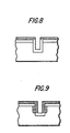
- An approach for manufacturing this structure is shown in Figs. 7 and 8. Isolation atthe bottom of the trench is achieved, for example, by etching the trench at 20a of Fig. 7 anisotropically to remove the implanted region at the bottom of the trench.
- doping of the sidewalls results from impurities ascending the sidewall from the bottom of the trench as well as descending from the top. As shown in Figs. 8 and 9 it can be sufficient to dope the sidewalls primarily from the top of the trench.
- trench-isolated devices For an n-channel trench-isolated structure, the sidewall doping is boron at a level of the order of 2x10¹⁶/cm3. Further details on trench isolation using conventional doping methods can be found in US-A-4104086 and US-A-4353086.
- layer 11 in this example includes a silicon nitride layer deposited on a silicon dioxide layer.
- a structure similar to that shown in Fig. 1 is formed by RIE etching a trench 1 11m wide and 5 1 1m deep.
- Layer 11 consists of 17,5 nm (175A) of grown oxide covered with 120 nm (1200A) of silicon nitride.
- the polysilicon layer 13 is 100 nm (1000A) thick and is deposited by conventional CVD.
- the polysilicon layer is capped with 70 nm (700A) of undoped oxide. The cap is optional (hence is not shown) and is recommended to obtain the desired implant profile in the transfer layer and to minimize evaporation of impurities during subsequent heat treatments.
- Boron is then implanted at 40 keV and 10 13 / CM 2 , followed by a drive-in step in nitrogen at 950 °C for 60 min.
- the polysilicon transfer layer is then oxidized through followed by an anneal at 950 °C for 60 min.
- the transfer layer, now converted to oxide, may remain in place. If desired the trench may be filled with dielectric material as described in US-A-4104086.
- the doping technique set forth herein has been described in terms of doping a sidewall.
- the method can be used for doping a layer or portion of a layer that is relatively inaccessible to the implant beam.
- a layer or region might, for example, be situated underneath another layer, in which case a portion of a transfer layer that is accessible to the beam is implanted and the implanted impurities are thereafter diffused to a region of the transfer layer that is inaccessible to the ion beam.
- the region of the transfer layer that is implanted will lie in one dimensional plane, typically normal or approximately normal to the ion implant beam, and the region to which the impurities are to be transferred may be along a vertical, or approximately vertical, plane inaccessible, or largely inaccessible to the ion beam, as in the case of the sidewalls described herein. Or the region to which the impurities are transferred may lie transversely with respect to the beam but inaccessible thereto due to intervening layers.
- Means for introducing the impurities may be by ion implantation or by predeposit from a gas or vapor source, both cases followed typically by a thermal treatment.
- the site where the impurities are desired is typically inaccessible, or not conveniently accessible, to the conventional source of impurities.
- Other situations where the invention is useful are where the site underlies one or more physical layers, making the site inaccessible to either an ion beam or a gas or vapor impurity source.
- Difficulties may arise in some applications of the so-called trench technology due to effects occurring at the bottom of the trench.
- layers deposited or formed at the bottom of the trench may exhibit non-uniformities. Since electric field effects are likely to be non-uniform in the vicinity of the corners of the trench, the potential for dielectric breakdown and other device failures is liable to be increased due to the corners and/or bottom of the trench. Moreover, stress effects within the substrate at these corners may encourage leakage of charge stored in the vicinity of the trench bottom. Therefore, it is sometimes advantageous, depending upon the particular devices being made, to utilize a structure like that shown in Figs. 7 and 9 in which the storage layer does not extend to, or around, the corners of the trench bottom.
Landscapes
- Semiconductor Integrated Circuits (AREA)
- Semiconductor Memories (AREA)
- Element Separation (AREA)
Abstract
Claims (11)
Applications Claiming Priority (2)
| Application Number | Priority Date | Filing Date | Title |
|---|---|---|---|
| US06/596,850 US4569701A (en) | 1984-04-05 | 1984-04-05 | Technique for doping from a polysilicon transfer layer |
| US596850 | 1996-02-05 |
Publications (2)
| Publication Number | Publication Date |
|---|---|
| EP0174997A1 EP0174997A1 (fr) | 1986-03-26 |
| EP0174997B1 true EP0174997B1 (fr) | 1988-08-03 |
Family
ID=24388981
Family Applications (1)
| Application Number | Title | Priority Date | Filing Date |
|---|---|---|---|
| EP85901826A Expired EP0174997B1 (fr) | 1984-04-05 | 1985-03-25 | Procede de dopage regule des parois laterales d'une tranchee dans un corps de semi-conducteur |
Country Status (6)
| Country | Link |
|---|---|
| US (1) | US4569701A (fr) |
| EP (1) | EP0174997B1 (fr) |
| JP (1) | JPS61501809A (fr) |
| CA (1) | CA1230431A (fr) |
| DE (1) | DE3564165D1 (fr) |
| WO (1) | WO1985004760A1 (fr) |
Families Citing this family (66)
| Publication number | Priority date | Publication date | Assignee | Title |
|---|---|---|---|---|
| GB2104722B (en) * | 1981-06-25 | 1985-04-24 | Suwa Seikosha Kk | Mos semiconductor device and method of manufacturing the same |
| JPS6181653A (ja) * | 1984-09-28 | 1986-04-25 | Nec Corp | 半導体装置の自己整合誘電体分離方法 |
| US4694561A (en) * | 1984-11-30 | 1987-09-22 | American Telephone And Telegraph Company, At&T Bell Laboratories | Method of making high-performance trench capacitors for DRAM cells |
| US4698104A (en) * | 1984-12-06 | 1987-10-06 | Xerox Corporation | Controlled isotropic doping of semiconductor materials |
| US4666557A (en) * | 1984-12-10 | 1987-05-19 | Ncr Corporation | Method for forming channel stops in vertical semiconductor surfaces |
| US4676847A (en) * | 1985-01-25 | 1987-06-30 | American Telephone And Telegraph Company At&T Bell Laboratories | Controlled boron doping of silicon |
| US4604150A (en) * | 1985-01-25 | 1986-08-05 | At&T Bell Laboratories | Controlled boron doping of silicon |
| JPS61202426A (ja) * | 1985-03-05 | 1986-09-08 | Matsushita Electric Ind Co Ltd | 半導体装置の製造方法 |
| US4627883A (en) * | 1985-04-01 | 1986-12-09 | Gte Laboratories Incorporated | Method of forming an isolated semiconductor structure |
| JPS61258468A (ja) * | 1985-05-13 | 1986-11-15 | Hitachi Ltd | 半導体記憶装置およびその製造方法 |
| US4653177A (en) * | 1985-07-25 | 1987-03-31 | At&T Bell Laboratories | Method of making and selectively doping isolation trenches utilized in CMOS devices |
| DE3686878T2 (de) * | 1985-07-25 | 1993-02-25 | American Telephone & Telegraph | Dram-arrays hoher leistung mit graben-kondensatoren. |
| US4889492A (en) * | 1986-05-07 | 1989-12-26 | Motorola, Inc. | High capacitance trench capacitor and well extension process |
| EP0259629A1 (fr) * | 1986-08-19 | 1988-03-16 | Siemens Aktiengesellschaft | Procédé pour fabriquer un dopage défini dans les parois latérales et les fonds des fossés creusés dans des substrats semi-conducteurs |
| US4782036A (en) * | 1986-08-29 | 1988-11-01 | Siemens Aktiengesellschaft | Process for producing a predetermined doping in side walls and bases of trenches etched into semiconductor substrates |
| JPH01287956A (ja) * | 1987-07-10 | 1989-11-20 | Toshiba Corp | 半導体記憶装置およびその製造方法 |
| JPH0644559B2 (ja) * | 1987-09-04 | 1994-06-08 | 株式会社東芝 | 半導体集積回路の製造方法 |
| US4871689A (en) * | 1987-11-17 | 1989-10-03 | Motorola Inc. | Multilayer trench isolation process and structure |
| US5354710A (en) * | 1988-01-14 | 1994-10-11 | Kabushiki Kaisha Toshiba | Method of manufacturing semiconductor devices using an adsorption enhancement layer |
| US5100823A (en) * | 1988-02-29 | 1992-03-31 | Motorola, Inc. | Method of making buried stacked transistor-capacitor |
| US4839309A (en) * | 1988-03-30 | 1989-06-13 | American Telephone And Telegraph Company, At&T Technologies, Inc. | Fabrication of high-speed dielectrically isolated devices utilizing buried silicide outdiffusion |
| KR920000708B1 (ko) * | 1988-07-22 | 1992-01-20 | 현대전자산업 주식회사 | 포토레지스트 에치백 기술을 이용한 트렌치 캐패시터 형성방법 |
| JP2593524B2 (ja) * | 1988-07-25 | 1997-03-26 | 株式会社東芝 | 半導体装置の製造方法 |
| KR910008830B1 (ko) * | 1988-08-18 | 1991-10-21 | 현대전자산업 주식회사 | 산화물벽과 질화물벽을 이용한 트렌치 측면벽 도핑방법 및 그 반도체 소자 |
| US5182224A (en) * | 1988-09-22 | 1993-01-26 | Hyundai Electronics Industries Co., Ltd. | Method of making dynamic random access memory cell having a SDHT structure |
| JP2733271B2 (ja) * | 1988-12-23 | 1998-03-30 | シャープ株式会社 | 半導体装置の製造方法 |
| US5084418A (en) * | 1988-12-27 | 1992-01-28 | Texas Instruments Incorporated | Method of making an array device with buried interconnects |
| US5264381A (en) * | 1989-01-18 | 1993-11-23 | Mitsubishi Denki Kabushiki Kaisha | Method of manufacturing a static induction type switching device |
| US5143859A (en) * | 1989-01-18 | 1992-09-01 | Mitsubishi Denki Kabushiki Kaisha | Method of manufacturing a static induction type switching device |
| US5026663A (en) * | 1989-07-21 | 1991-06-25 | Motorola, Inc. | Method of fabricating a structure having self-aligned diffused junctions |
| JP2641781B2 (ja) * | 1990-02-23 | 1997-08-20 | シャープ株式会社 | 半導体素子分離領域の形成方法 |
| US5296392A (en) * | 1990-03-06 | 1994-03-22 | Digital Equipment Corporation | Method of forming trench isolated regions with sidewall doping |
| EP0505877A2 (fr) * | 1991-03-27 | 1992-09-30 | Seiko Instruments Inc. | Méthode de dopage à l'aide d'une source de diffusion adsorbée |
| US5229322A (en) * | 1991-12-05 | 1993-07-20 | International Business Machines Corporation | Method of making low resistance substrate or buried layer contact |
| US5324684A (en) * | 1992-02-25 | 1994-06-28 | Ag Processing Technologies, Inc. | Gas phase doping of semiconductor material in a cold-wall radiantly heated reactor under reduced pressure |
| US5350941A (en) * | 1992-09-23 | 1994-09-27 | Texas Instruments Incorporated | Trench isolation structure having a trench formed in a LOCOS structure and a channel stop region on the sidewalls of the trench |
| DE59409300D1 (de) * | 1993-06-23 | 2000-05-31 | Siemens Ag | Verfahren zur Herstellung von einem Isolationsgraben in einem Substrat für Smart-Power-Technologien |
| DE59405680D1 (de) * | 1993-06-23 | 1998-05-20 | Siemens Ag | Verfahren zur Herstellung eines Isolationsgrabens in einem Substrat für Smart-Power-Technologien |
| US5416041A (en) * | 1993-09-27 | 1995-05-16 | Siemens Aktiengesellschaft | Method for producing an insulating trench in an SOI substrate |
| US5451809A (en) * | 1994-09-07 | 1995-09-19 | Kabushiki Kaisha Toshiba | Smooth surface doped silicon film formation |
| US6228750B1 (en) | 1994-12-30 | 2001-05-08 | Lucent Technologies | Method of doping a semiconductor surface |
| JP2636796B2 (ja) * | 1995-05-24 | 1997-07-30 | 日本電気株式会社 | 半導体装置の製造方法 |
| KR0179807B1 (ko) * | 1995-12-30 | 1999-03-20 | 문정환 | 반도체 기억소자 제조방법 |
| KR100244271B1 (ko) * | 1997-05-06 | 2000-02-01 | 김영환 | 반도체소자 구조 및 제조방법 |
| AT2173U1 (de) * | 1997-06-19 | 1998-05-25 | Austria Mikrosysteme Int | Verfahren zur herstellung von begrenzten, dotierten teilgebieten in einem substratmaterial aus monokristallinem silizium |
| US6107135A (en) * | 1998-02-11 | 2000-08-22 | Kabushiki Kaisha Toshiba | Method of making a semiconductor memory device having a buried plate electrode |
| GB2344215B (en) * | 1998-11-26 | 2003-10-08 | Siemens Plc | Method of forming a buried plate |
| US6891209B2 (en) * | 2001-08-13 | 2005-05-10 | Amberwave Systems Corporation | Dynamic random access memory trench capacitors |
| US7736976B2 (en) * | 2001-10-04 | 2010-06-15 | Vishay General Semiconductor Llc | Method for fabricating a power semiconductor device having a voltage sustaining layer with a terraced trench facilitating formation of floating islands |
| US6465304B1 (en) | 2001-10-04 | 2002-10-15 | General Semiconductor, Inc. | Method for fabricating a power semiconductor device having a floating island voltage sustaining layer |
| US6576516B1 (en) * | 2001-12-31 | 2003-06-10 | General Semiconductor, Inc. | High voltage power MOSFET having a voltage sustaining region that includes doped columns formed by trench etching and diffusion from regions of oppositely doped polysilicon |
| US6656797B2 (en) | 2001-12-31 | 2003-12-02 | General Semiconductor, Inc. | High voltage power MOSFET having a voltage sustaining region that includes doped columns formed by trench etching and ion implantation |
| US6566201B1 (en) | 2001-12-31 | 2003-05-20 | General Semiconductor, Inc. | Method for fabricating a high voltage power MOSFET having a voltage sustaining region that includes doped columns formed by rapid diffusion |
| US6750104B2 (en) | 2001-12-31 | 2004-06-15 | General Semiconductor, Inc. | High voltage power MOSFET having a voltage sustaining region that includes doped columns formed by trench etching using an etchant gas that is also a doping source |
| US6686244B2 (en) * | 2002-03-21 | 2004-02-03 | General Semiconductor, Inc. | Power semiconductor device having a voltage sustaining region that includes doped columns formed with a single ion implantation step |
| TWI230456B (en) * | 2003-05-14 | 2005-04-01 | Promos Technologies Inc | Shallow trench isolation and dynamic random access memory and fabricating methods thereof |
| JP5110776B2 (ja) * | 2004-07-01 | 2012-12-26 | セイコーインスツル株式会社 | 半導体装置の製造方法 |
| KR100685620B1 (ko) * | 2006-02-16 | 2007-02-22 | 주식회사 하이닉스반도체 | 반도체 소자 및 그 제조 방법 |
| KR100769146B1 (ko) * | 2006-08-17 | 2007-10-22 | 동부일렉트로닉스 주식회사 | 전기적 특성을 향상시키는 반도체 소자 및 그 제조 방법 |
| JP2011249354A (ja) * | 2010-05-21 | 2011-12-08 | Sharp Corp | 半導体装置の製造方法 |
| US8940388B2 (en) | 2011-03-02 | 2015-01-27 | Micron Technology, Inc. | Insulative elements |
| US9111853B2 (en) * | 2013-03-15 | 2015-08-18 | Micron Technology, Inc. | Methods of forming doped elements of semiconductor device structures |
| CN106328503B (zh) * | 2015-06-30 | 2019-08-27 | 中芯国际集成电路制造(上海)有限公司 | 半导体结构的形成方法 |
| US10522549B2 (en) * | 2018-02-17 | 2019-12-31 | Varian Semiconductor Equipment Associates, Inc. | Uniform gate dielectric for DRAM device |
| US11361991B2 (en) * | 2018-03-09 | 2022-06-14 | Applied Materials, Inc. | Method for Si gap fill by PECVD |
| US10937654B2 (en) * | 2019-01-24 | 2021-03-02 | Micron Technology, Inc. | Methods of doping a silicon-containing material and methods of forming a semiconductor device |
Family Cites Families (12)
| Publication number | Priority date | Publication date | Assignee | Title |
|---|---|---|---|---|
| US4074304A (en) * | 1974-10-04 | 1978-02-14 | Nippon Electric Company, Ltd. | Semiconductor device having a miniature junction area and process for fabricating same |
| DE2449688C3 (de) * | 1974-10-18 | 1980-07-10 | Siemens Ag, 1000 Berlin Und 8000 Muenchen | Verfahren zur Herstellung einer dotierten Zone eines Leitfähigkeitstyps in einem Halbleiterkörper |
| US4016587A (en) * | 1974-12-03 | 1977-04-05 | International Business Machines Corporation | Raised source and drain IGFET device and method |
| US4026733A (en) * | 1975-10-29 | 1977-05-31 | Intel Corporation | Process for defining polycrystalline silicon patterns |
| US4104086A (en) * | 1977-08-15 | 1978-08-01 | International Business Machines Corporation | Method for forming isolated regions of silicon utilizing reactive ion etching |
| US4239559A (en) * | 1978-04-21 | 1980-12-16 | Hitachi, Ltd. | Method for fabricating a semiconductor device by controlled diffusion between adjacent layers |
| US4389255A (en) * | 1980-01-14 | 1983-06-21 | Burroughs Corporation | Method of forming buried collector for bipolar transistor in a semiconductor by selective implantation of poly-si followed by oxidation and etch-off |
| US4353086A (en) * | 1980-05-07 | 1982-10-05 | Bell Telephone Laboratories, Incorporated | Silicon integrated circuits |
| US4397075A (en) * | 1980-07-03 | 1983-08-09 | International Business Machines Corporation | FET Memory cell structure and process |
| US4325182A (en) * | 1980-08-25 | 1982-04-20 | General Electric Company | Fast isolation diffusion |
| GB2104722B (en) * | 1981-06-25 | 1985-04-24 | Suwa Seikosha Kk | Mos semiconductor device and method of manufacturing the same |
| US4431460A (en) * | 1982-03-08 | 1984-02-14 | International Business Machines Corporation | Method of producing shallow, narrow base bipolar transistor structures via dual implantations of selected polycrystalline layer |
-
1984
- 1984-04-05 US US06/596,850 patent/US4569701A/en not_active Expired - Lifetime
-
1985
- 1985-03-25 JP JP60501521A patent/JPS61501809A/ja active Granted
- 1985-03-25 EP EP85901826A patent/EP0174997B1/fr not_active Expired
- 1985-03-25 WO PCT/US1985/000503 patent/WO1985004760A1/fr not_active Ceased
- 1985-03-25 DE DE8585901826T patent/DE3564165D1/de not_active Expired
- 1985-04-04 CA CA000478431A patent/CA1230431A/fr not_active Expired
Also Published As
| Publication number | Publication date |
|---|---|
| JPH0560649B2 (fr) | 1993-09-02 |
| WO1985004760A1 (fr) | 1985-10-24 |
| DE3564165D1 (en) | 1988-09-08 |
| US4569701A (en) | 1986-02-11 |
| JPS61501809A (ja) | 1986-08-21 |
| CA1230431A (fr) | 1987-12-15 |
| EP0174997A1 (fr) | 1986-03-26 |
Similar Documents
| Publication | Publication Date | Title |
|---|---|---|
| CA1230431A (fr) | Technique de dopage a partir d'une couche de transfert a polysilicium | |
| US4604150A (en) | Controlled boron doping of silicon | |
| EP0066081B1 (fr) | Transistor à effet de champ vertical à grande densité et procédé pour sa fabrication | |
| US4676847A (en) | Controlled boron doping of silicon | |
| US6177696B1 (en) | Integration scheme enhancing deep trench capacitance in semiconductor integrated circuit devices | |
| KR100202278B1 (ko) | 반도체 메모리 장치내 매설 스트랩의 제어된 재결정화 | |
| US4833094A (en) | Method of making a dynamic ram cell having shared trench storage capacitor with sidewall-defined bridge contacts and gate electrodes | |
| JP2705716B2 (ja) | Dramセルの製造方法 | |
| EP0264858B1 (fr) | Cellule de mémoire du type RAM comprenant un condensateur de stockage commun dans un sillon, dont les parois déterminent les contacts à pont et les électrodes de porte | |
| US5821629A (en) | Buried structure SRAM cell and methods for fabrication | |
| US6218236B1 (en) | Method of forming a buried bitline in a vertical DRAM device | |
| US6846744B1 (en) | Method of fabricating a bottle shaped deep trench for trench capacitor DRAM devices | |
| US5026659A (en) | Process for fabricating stacked trench capacitors of dynamic ram | |
| KR100530932B1 (ko) | 집적회로제조방법 | |
| US6933215B2 (en) | Process for doping a semiconductor body | |
| US6420750B1 (en) | Structure and method for buried-strap with reduced outdiffusion | |
| US20030109140A1 (en) | Buried strap formation method for sub-150 nm best DRAM devices | |
| US6677197B2 (en) | High aspect ratio PBL SiN barrier formation | |
| KR20000017093A (ko) | 반도체 장치 | |
| US5899716A (en) | Oxygen ion implantation procedure to increase the surface area of an STC structure | |
| US6436760B1 (en) | Method for reducing surface oxide in polysilicon processing | |
| US5472902A (en) | Silicon-on-insulator isolation technology using liquid phase deposition | |
| US6492282B1 (en) | Integrated circuits and manufacturing methods | |
| KR100476603B1 (ko) | 트렌치형 dram 셀의 보다 높은 충전 유지 시간을 위한페디스털 칼라 구조 | |
| US5534457A (en) | Method of forming a stacked capacitor with an "I" shaped storage node |
Legal Events
| Date | Code | Title | Description |
|---|---|---|---|
| PUAI | Public reference made under article 153(3) epc to a published international application that has entered the european phase |
Free format text: ORIGINAL CODE: 0009012 |
|
| AK | Designated contracting states |
Kind code of ref document: A1 Designated state(s): DE FR GB NL |
|
| 17P | Request for examination filed |
Effective date: 19860326 |
|
| 17Q | First examination report despatched |
Effective date: 19870407 |
|
| GRAA | (expected) grant |
Free format text: ORIGINAL CODE: 0009210 |
|
| AK | Designated contracting states |
Kind code of ref document: B1 Designated state(s): DE FR GB NL |
|
| REF | Corresponds to: |
Ref document number: 3564165 Country of ref document: DE Date of ref document: 19880908 |
|
| ET | Fr: translation filed | ||
| PLBE | No opposition filed within time limit |
Free format text: ORIGINAL CODE: 0009261 |
|
| STAA | Information on the status of an ep patent application or granted ep patent |
Free format text: STATUS: NO OPPOSITION FILED WITHIN TIME LIMIT |
|
| 26N | No opposition filed | ||
| PGFP | Annual fee paid to national office [announced via postgrant information from national office to epo] |
Ref country code: GB Payment date: 20010226 Year of fee payment: 17 |
|
| PGFP | Annual fee paid to national office [announced via postgrant information from national office to epo] |
Ref country code: NL Payment date: 20010312 Year of fee payment: 17 |
|
| PGFP | Annual fee paid to national office [announced via postgrant information from national office to epo] |
Ref country code: DE Payment date: 20010330 Year of fee payment: 17 |
|
| REG | Reference to a national code |
Ref country code: GB Ref legal event code: IF02 |
|
| PG25 | Lapsed in a contracting state [announced via postgrant information from national office to epo] |
Ref country code: GB Free format text: LAPSE BECAUSE OF NON-PAYMENT OF DUE FEES Effective date: 20020325 |
|
| PG25 | Lapsed in a contracting state [announced via postgrant information from national office to epo] |
Ref country code: NL Free format text: LAPSE BECAUSE OF NON-PAYMENT OF DUE FEES Effective date: 20021001 Ref country code: DE Free format text: LAPSE BECAUSE OF NON-PAYMENT OF DUE FEES Effective date: 20021001 |
|
| GBPC | Gb: european patent ceased through non-payment of renewal fee |
Effective date: 20020325 |
|
| NLV4 | Nl: lapsed or anulled due to non-payment of the annual fee |
Effective date: 20021001 |
|
| PGFP | Annual fee paid to national office [announced via postgrant information from national office to epo] |
Ref country code: FR Payment date: 20040507 Year of fee payment: 20 |