EP0175080A2 - Mémoire de micro-ordinateur et son procédé de fonctionnement - Google Patents
Mémoire de micro-ordinateur et son procédé de fonctionnement Download PDFInfo
- Publication number
- EP0175080A2 EP0175080A2 EP85108699A EP85108699A EP0175080A2 EP 0175080 A2 EP0175080 A2 EP 0175080A2 EP 85108699 A EP85108699 A EP 85108699A EP 85108699 A EP85108699 A EP 85108699A EP 0175080 A2 EP0175080 A2 EP 0175080A2
- Authority
- EP
- European Patent Office
- Prior art keywords
- bank
- memory
- row
- cache
- distributed cache
- Prior art date
- Legal status (The legal status is an assumption and is not a legal conclusion. Google has not performed a legal analysis and makes no representation as to the accuracy of the status listed.)
- Granted
Links
Images


Classifications
-
- G—PHYSICS
- G06—COMPUTING OR CALCULATING; COUNTING
- G06F—ELECTRIC DIGITAL DATA PROCESSING
- G06F12/00—Accessing, addressing or allocating within memory systems or architectures
- G06F12/02—Addressing or allocation; Relocation
- G06F12/08—Addressing or allocation; Relocation in hierarchically structured memory systems, e.g. virtual memory systems
- G06F12/0802—Addressing of a memory level in which the access to the desired data or data block requires associative addressing means, e.g. caches
- G06F12/0893—Caches characterised by their organisation or structure
Definitions
- the present invention is generally related to memory systems for microcomputers, and more particularly to a memory controller for static column mode dynamic random access memories (DRAMs) which significantly improves system performance.
- DRAMs static column mode dynamic random access memories
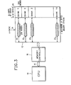
- a typical microcomputer system has the central processing unit (CPU) 10 connected to the memory 12 over a bus 14 as shown in Figure 1.
- CPU central processing unit
- the memory controller 18 performs the task of refreshing the DRAMs, bank interleaving, clocking and handshake protocol with the CPU 10.
- Some microcomputers also have an instruction and/or data cache 20 to increase system throughput.
- the cache is a fast memory, and it normally resides on the CPU side of the bus.
- the control logic associated with the cache attempts to maximize the number of accesses to the cache. An access to the cache is termed a "hit".
- the main memory is accessed only when the desired 'word is not available in the cache, i.e. a "miss".
- DRAMs with static column mode now offered by some manufacturers represents a new trend in dynamic memories. They have an on-chip static buffer for storing an entire row '(256 bits for a 64 Kbit DRAM chip).
- a 64K DRAM has 256 rows of 256 bits each.
- a 256K DRAM has 512 rows of 512 bits each, whereas a 64K by 4 DRAM has 4 times 256 rows of 256 bits.
- the objects of the invention are attained by organizing a microcomputer memory system into a plurality of banks, each bank consisting of an array of static-column mode dynamic random access memories of the type having an on-chip static buffer for storing an entire row.
- the static buffers associated with each bank are used as a distributed cache to hold the last accessed row for the associated bank.
- a memory controller receives real addresses on the memory bus and extracts bank and row numbers from the address. The memory controller determines whether the accessed row for a memory bank is in the distributed cache and, if it is, accesses the distributed cache for that bank. Otherwise, the memory controller switches the contents of the distributed cache with the contents of the addressed row for that bank. Because access times to the static buffers are very short, a significant increase in system performance is achieved.
- the static buffer on the DRAM can be looked upon as an on-chip cache for the currently addressed row. If a new access requires a bit from a different row, the old one in buffer is written back into the DRAM cell matrix and the new one loaded into the buffer automatically in just 130 ns. Thus, operation is at 40 ns. from the static buffer with occasional overhead of 13G ns. when the buffered row has to be switched, these figures being typical for currently available DRAMs.
- the memory 12 is orgainized in sixteen banks with each bank consisting of an array of eight 64K by 4 DRAMs. Each bank has a 256 word or 1K byte static buffer 22 1 to 22 16 .
- the static buffers associated with the banks are referred to as "d-cache" 24 for distributed cache.
- the d-cache 24 is a fast access buffer associated with the bank. It holds the last accessed row for the associated bank. It should be noted that the d-cache is physically on the DRAM chips and is not added externally to the system. Moreover, it caches everything, including data, instructions, stack and so forth.
- the term "distributed" empnasizes two aspects of the invention. First, the d-cache is not tightly coupled to the CPU but is on the memory side of the system, and second, a unit of d-cache is strictly associated with a definite memory bank.
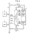
- Figure 4 shows the memory 12 in more generalized form organized into a plurality of banks numbered 1 to n.
- Figure 4 also shows in more detail the input and output signal lines of the memory controller 18.
- the memory controller 18 receives real addresses from the CPU 10 (or some other DMA unit 24 on the bus 14) and accesses the DRAMs for read or write operation. It does the refreshing of the DRAMs. It also keeps track of the row of each bank currently cached in the d-cache.
- the memory controller also maintains all the timing for the DRAMs in terms of refresh and access times. It also provides for the - proper handshake protocol with the bus. For each bank, the memory controller maintains two fields, the number of the row which is currently in the d-cache and a valid entry flag for the d-cache as shown in the table below:
- the DRAMs use the buffer also during the refresh operation, destroying the d-cache contents. Thus, the valid bits are also set to 0 following a refresh operation in a bank.
- the memory controller On being accessed from the bus, the memory controller extracts the bank and row numbers from the address.
- the physical address break-up is as follows:
- the memory controller 18 determines if the accessed row for that bank is already in the d-cache (a hit). If it is, then the memory controller sends out the column address (position within the d-cache) and activates the column address select (CAS) line for that bank. An active CAS for a bank selects that bank for access. Such a hit access is very fast, on the order of 35 to 40 ns. If the accessed word is not in the d-cache (a miss), then the contents of the d-cache have to be switched. To do that, the row address select (RAS) for that bank is made inactive and made active again with the row number of the new address.
- RAS row address select
- This operation takes only 130 ns., writes back the d-cache contents into the DRAM cell matrix and loads the entire new row into the d-cache. This extremely short time needed to switch the entire d-cache contents is one of the major reasons for the good performance of the invention.
- the accessed word is read into latch 26 from memory 12 and strobed to the bus 14 by the memory controller 18 in the usual manner.
- the refresh operation is imperative for any dynamic RAM.
- Standard DRAMs require total refreshing (all rows) once every 4 milliseconds. with 256 rows, a row in a bank has to be refreshed, on an average, every 16 microseconds. Since a refresh operation destroys the d-cache contents, every 16 microseconds, the d-cache is declared invalid and the first access following refresh will be a miss. Thus, the d-cache maximum life expectancy, due to refresh, is 16 nicroseconds. With the availability of extended refresh (64 milliseconds) DRAMs, this is improved to 256 microseconds. To improve the overall system performance, same row numbers of all banks are refreshed simultaneously. This means a total of 256 refresh operations in 4 milliseconds are needed for the entire memory, independent of the number of banks.
- the refresh operation by itself consists of making the RAS line active and once again making the RAS line inactive. It lasts 130 ns.
- the memory controller can address up to 16 banks of memory. With each bank containing 64K words (255K bytes), this amounts to one megaword (4 M bytes). This also gives a total of up to 4K words (16K bytes) of d-cache. Since one memory bank yields only one d-cache block, to have more d-cache it is very important to have the total memory broken up in a number of memory banks. 64K by 4 configuration of 256K DRAMs result in more banks than the 256K by 1 configuration.
- the memory controller as shown in Figure 4 keeps d-cache for all the banks active or ready for fast access by keeping the RAS line for each bank active. It uses the CAS lines to select the bank it wants to access.
- the entire currently used work area (code, data, stack and etc.) .of the program can be in d-cache.
- An additional benefit of multiple memory banks is that one or more redundant memory banks could be supported and brought into action if it is detected that one of the currently running banks has failed.
- the memory controller can dynamically map the bank number from the processor to the ones currently operating.
- FIG. 5 shows a block diagram of the memory controller 18.
- the bus control unit 28 interfaces with the system bus 14. It receives real addresses and sends and receives data to and from the system bus. All transactions with the CPU or other units on the system bus are synchronized with the bus clock by the timing and control circuitry 30.
- the CPU or other system bus units can access the memory controller 18 every bus cycle with a new read or write request. If the memory controller is busy and can not accept a request, the bus control unit 28 sends back a RETRY signal asking the requesting unit to repeat the request in the following cycle. If the memory controller 18 is ready to send back the data for a previous request, the bus controller informs systems bus units one cycle in advance so as to reserve the system bus for data transmission. Any request for read or write may take an unknown number of cycles to be processed by tne memory controller depending on a number of conditions such as refresh, d-cache hit or miss and the like, but the sequence of execution is strictly the same as the sequence of requests.
- a set of buffers 32 and address registers 34 are provided in order to maintain a pipelined flow of addresses and data from the system bus to the d-cache manager 36 and the error checking and correcting (ECC) unit 38 on the one hand, and from the ECC unit 38 to the system bus 14 on the other.
- the d-cache manager 36 interfaces with the refresh controller 40 to provide the required refresh to the DRAM chips in each of the banks in the memory.
- the d-cache manager interfaces to a 32-bit bus on the DRAM side and drives up to sixteen memory banks. Each bank is made up of ten or forty memory chips (depending on whether the chips are organized "by 1" or "by 4") comprising 32-bit wide memory with bits for ECC.
- the d-cache manager 36 maintains a row address table which keeps track of the active row addresses in each memory bank. The addresses of all load/store requests are compared against the entries in this table to determine if a fast access is possiole or not.
- the d-cache manager 36 has one pair of RAS/CAS lines for each bank. Row access strobe (RAS) is used to load and unload DRAM rows into the row buffer (d-cache), and column access strobe (CAS) is used to select the bank.
- RAS Row access strobe
- CAS column access strobe
- the memory clock is asynchronous to the bus clock and is selected to optimize the access time to the DRAMS.
- the bus clock is selected to match the processor speed.
- the refresh controller 40 contains a refresh counter that cycles through the row addresses for all rows on the DRAMs. There is also a clock counter which signals a refresh period. At each such refresh period, the row pointed to by the contents of the refresh counter is refreshed in every DRAM in the system, and the refresh counter is incremented in preparation for the next refresh. When refresh occurs, the contents of the row address table in the d-cache manager is invalidiated.
- the ECC unit 38 does a pass-through generation, checking and correcting errors. Single bit errors are corrected and flagged for recording purposes. Douole bit errors are signaled to the units on the system bus.
- the buffer, RAM access and ECC occur in a pipelined fashion and 'hence once the pipeline is loaded and running, one access per bus cycle is achieved.
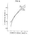
- Performance studies were done on models of a 32 bit microprocessor coupled to a memory system.
- a PL/1 type compilation was used as a benchmark program. The purpose was to determine how the number of banks of DRAMs effect performance and d-cache hit ratios. Also evaluated was the effect of a processor with 1/2-Kbyte and 1-Kbyte on-chip instruction cache coupled with the static column DRAMs.
- the first column in the above table is the relative performance figures for no on-chip cache.
- the second column is the relative performance figures for 1/2-K byte of I-cache, and the third column is for 1K byte of I-cache.
- Figure 6 shows the d-cacne hit ratio. From these performance studies, several conclusions can be drawn. First, the d-cache DRAMs offer a substantial performance advantage over standard DRAMs. Second, the performance of microprocessors with I-cache improves significantly with d-cache DRAMs. Third, the performance is a function of the number of memory banks since the amount of d-cache available increases with the number of banks. Thus, higher performance results from partitioning the available amount of memory into a large number of banks. Fourth, the performance of a system without I-cache can, in fact, be better than one with I-cache. This is because I-cache requires an overhead of sequentially loaoing the cacne buffer, at times with words whicn may never be used.
- a d-cache has literally zero operating overhead because the time to load the d-cache is the same as that to access the first word in it. Another reason for better performance is 'that d-cache caches literally all types of information, code, data, stack, etc. Thus, access to every type of information is speeded up.
- the hit ratios on d-cache is very high. It is the ratio of fast accesses to total accesses. The hit ratio increases with the number of memory banks for both cases, with and without on chip I-cache. This is because the amount of d-cache available increases with the number of banks.
- DRAMs with static column mode when used with the memory controller according to the invention can significantly improve (by more than 50%) system performance beyond that of systems with standard DRAMs, even with on chip I-cacne.
Landscapes
- Engineering & Computer Science (AREA)
- Theoretical Computer Science (AREA)
- Physics & Mathematics (AREA)
- General Engineering & Computer Science (AREA)
- General Physics & Mathematics (AREA)
- Memory System Of A Hierarchy Structure (AREA)
- Dram (AREA)
- Memory System (AREA)
Applications Claiming Priority (2)
| Application Number | Priority Date | Filing Date | Title |
|---|---|---|---|
| US06/651,562 US4725945A (en) | 1984-09-18 | 1984-09-18 | Distributed cache in dynamic rams |
| US651562 | 1984-09-18 |
Publications (3)
| Publication Number | Publication Date |
|---|---|
| EP0175080A2 true EP0175080A2 (fr) | 1986-03-26 |
| EP0175080A3 EP0175080A3 (en) | 1988-07-27 |
| EP0175080B1 EP0175080B1 (fr) | 1991-11-13 |
Family
ID=24613332
Family Applications (1)
| Application Number | Title | Priority Date | Filing Date |
|---|---|---|---|
| EP85108699A Expired EP0175080B1 (fr) | 1984-09-18 | 1985-07-12 | Mémoire de micro-ordinateur et son procédé de fonctionnement |
Country Status (5)
| Country | Link |
|---|---|
| US (1) | US4725945A (fr) |
| EP (1) | EP0175080B1 (fr) |
| JP (1) | JPS6174041A (fr) |
| CA (1) | CA1233272A (fr) |
| DE (1) | DE3584656D1 (fr) |
Cited By (6)
| Publication number | Priority date | Publication date | Assignee | Title |
|---|---|---|---|---|
| FR2602070A1 (fr) * | 1986-07-24 | 1988-01-29 | Sun Microsystems Inc | Systeme et procede d'acces a une memoire d'ordinateur. |
| FR2627298A1 (fr) * | 1988-02-16 | 1989-08-18 | Sun Microsystems Inc | Systeme informatique a antememoire et procede pour acceder a des donnees dans un tel systeme |
| EP0239951A3 (en) * | 1986-03-31 | 1990-10-24 | Wang Laboratories Inc. | Pseudo-static memory subsystem |
| GB2244157A (en) * | 1990-05-15 | 1991-11-20 | Sun Microsystems Inc | Apparatus for row caching in random access memory |
| EP0468141A3 (en) * | 1990-07-23 | 1992-09-30 | International Business Machines Corporation | Memory |
| AU637616B2 (en) * | 1989-07-03 | 1993-06-03 | Tandem Computers Incorporated | Apparatus and method for reading, writing, and refreshing memory with direct virtual or physical access |
Families Citing this family (88)
| Publication number | Priority date | Publication date | Assignee | Title |
|---|---|---|---|---|
| JPS62103898A (ja) * | 1985-10-31 | 1987-05-14 | Mitsubishi Electric Corp | ダイナミツクランダムアクセスメモリ装置 |
| US5226136A (en) * | 1986-05-06 | 1993-07-06 | Nintendo Company Limited | Memory cartridge bank selecting apparatus |
| JPS62260244A (ja) * | 1986-05-06 | 1987-11-12 | Nintendo Co Ltd | メモリカ−トリツジ |
| CA1330596C (fr) * | 1986-11-19 | 1994-07-05 | Yoshiaki Nakanishi | Cartouche de memoire et appareil de traitement de donnees |
| JPS63175287A (ja) * | 1987-01-16 | 1988-07-19 | Hitachi Ltd | 記憶装置 |
| US4894770A (en) * | 1987-06-01 | 1990-01-16 | Massachusetts Institute Of Technology | Set associative memory |
| JP2714944B2 (ja) * | 1987-08-05 | 1998-02-16 | 三菱電機株式会社 | 半導体記憶装置 |
| US5179687A (en) * | 1987-09-26 | 1993-01-12 | Mitsubishi Denki Kabushiki Kaisha | Semiconductor memory device containing a cache and an operation method thereof |
| US5051889A (en) * | 1987-10-23 | 1991-09-24 | Chips And Technologies, Incorporated | Page interleaved memory access |
| US5226147A (en) * | 1987-11-06 | 1993-07-06 | Mitsubishi Denki Kabushiki Kaisha | Semiconductor memory device for simple cache system |
| JPH01146187A (ja) * | 1987-12-02 | 1989-06-08 | Mitsubishi Electric Corp | キヤッシュメモリ内蔵半導体記憶装置 |
| JPH01154261A (ja) * | 1987-12-11 | 1989-06-16 | Toshiba Corp | 情報処理装置 |
| US5146581A (en) * | 1988-02-24 | 1992-09-08 | Sanyo Electric Co., Ltd. | Subprogram executing data processing system having bank switching control storing in the same address area in each of memory banks |
| US5329489A (en) * | 1988-03-31 | 1994-07-12 | Texas Instruments Incorporated | DRAM having exclusively enabled column buffer blocks |
| JP2895488B2 (ja) | 1988-04-18 | 1999-05-24 | 株式会社東芝 | 半導体記憶装置及び半導体記憶システム |
| US5301278A (en) * | 1988-04-29 | 1994-04-05 | International Business Machines Corporation | Flexible dynamic memory controller |
| US4974146A (en) * | 1988-05-06 | 1990-11-27 | Science Applications International Corporation | Array processor |
| US4870622A (en) * | 1988-06-24 | 1989-09-26 | Advanced Micro Devices, Inc. | DRAM controller cache |
| US4939692A (en) * | 1988-09-15 | 1990-07-03 | Intel Corporation | Read-only memory for microprocessor systems having shared address/data lines |
| US4905141A (en) * | 1988-10-25 | 1990-02-27 | International Business Machines Corporation | Partitioned cache memory with partition look-aside table (PLAT) for early partition assignment identification |
| US6092153A (en) * | 1988-11-14 | 2000-07-18 | Lass; Stanley Edwin | Subsettable top level cache |
| CA2011518C (fr) * | 1989-04-25 | 1993-04-20 | Ronald N. Fortino | Puces de memoire vive dynamique avec antememoire repartie et methode de controle connexe |
| US5261073A (en) * | 1989-05-05 | 1993-11-09 | Wang Laboratories, Inc. | Method and apparatus for providing memory system status signals |
| US4967397A (en) * | 1989-05-15 | 1990-10-30 | Unisys Corporation | Dynamic RAM controller |
| US5138705A (en) * | 1989-06-26 | 1992-08-11 | International Business Machines Corporation | Chip organization for an extendable memory structure providing busless internal page transfers |
| JP2646032B2 (ja) * | 1989-10-14 | 1997-08-25 | 三菱電機株式会社 | Lifo方式の半導体記憶装置およびその制御方法 |
| JP2777247B2 (ja) * | 1990-01-16 | 1998-07-16 | 三菱電機株式会社 | 半導体記憶装置およびキャッシュシステム |
| DE69123987T2 (de) * | 1990-01-31 | 1997-04-30 | Hewlett Packard Co | Stossbetrieb für Mikroprozessor mit externem Systemspeicher |
| US5257360A (en) * | 1990-03-23 | 1993-10-26 | Advanced Micro Devices,Inc. | Re-configurable block length cache |
| JP2862948B2 (ja) * | 1990-04-13 | 1999-03-03 | 三菱電機株式会社 | 半導体記憶装置 |
| JP3225531B2 (ja) * | 1990-05-15 | 2001-11-05 | セイコーエプソン株式会社 | メモリカード |
| US5200564A (en) * | 1990-06-29 | 1993-04-06 | Casio Computer Co., Ltd. | Digital information processing apparatus with multiple CPUs |
| US5584034A (en) * | 1990-06-29 | 1996-12-10 | Casio Computer Co., Ltd. | Apparatus for executing respective portions of a process by main and sub CPUS |
| JPH0682339B2 (ja) * | 1990-08-31 | 1994-10-19 | インターナショナル・ビジネス・マシーンズ・コーポレイション | メモリ・アクセス・システムおよび方法 |
| DE69233510T2 (de) * | 1991-03-01 | 2006-02-02 | Advanced Micro Devices, Inc., Sunnyvale | Ausgangspuffer für Mikroprozessor |
| US5276838A (en) * | 1991-03-04 | 1994-01-04 | International Business Machines Corporation | Dynamically repositioned memory bank queues |
| US5289584A (en) * | 1991-06-21 | 1994-02-22 | Compaq Computer Corp. | Memory system with FIFO data input |
| JP2729423B2 (ja) * | 1991-10-29 | 1998-03-18 | 三菱電機株式会社 | 半導体記憶装置 |
| DE69324508T2 (de) * | 1992-01-22 | 1999-12-23 | Enhanced Memory Systems, Inc. | DRAM mit integrierten Registern |
| KR950000504B1 (ko) * | 1992-01-31 | 1995-01-24 | 삼성전자 주식회사 | 복수개의 로우 어드레스 스트로브 신호를 가지는 반도체 메모리 장치 |
| US5282177A (en) * | 1992-04-08 | 1994-01-25 | Micron Technology, Inc. | Multiple register block write method and circuit for video DRAMs |
| US5251174A (en) * | 1992-06-12 | 1993-10-05 | Acer Incorporated | Memory system |
| US5307320A (en) * | 1992-09-23 | 1994-04-26 | Intel Corporation | High integration DRAM controller |
| US5530902A (en) * | 1993-06-14 | 1996-06-25 | Motorola, Inc. | Data packet switching system having DMA controller, service arbiter, buffer type managers, and buffer managers for managing data transfer to provide less processor intervention |
| US5573629A (en) * | 1994-08-03 | 1996-11-12 | Herd Manufacturing, Inc. | Tape application apparatus |
| JP2704607B2 (ja) * | 1994-08-03 | 1998-01-26 | 三菱電機株式会社 | 半導体記憶装置 |
| US5508968A (en) * | 1994-08-12 | 1996-04-16 | International Business Machines Corporation | Dynamic random access memory persistent page implemented as processor register sets |
| AU5386796A (en) * | 1995-04-11 | 1996-10-30 | Kinetech, Inc. | Identifying data in a data processing system |
| US5787267A (en) * | 1995-06-07 | 1998-07-28 | Monolithic System Technology, Inc. | Caching method and circuit for a memory system with circuit module architecture |
| US5873114A (en) * | 1995-08-18 | 1999-02-16 | Advanced Micro Devices, Inc. | Integrated processor and memory control unit including refresh queue logic for refreshing DRAM during idle cycles |
| US5835941A (en) * | 1995-11-17 | 1998-11-10 | Micron Technology Inc. | Internally cached static random access memory architecture |
| US6567904B1 (en) | 1995-12-29 | 2003-05-20 | Intel Corporation | Method and apparatus for automatically detecting whether a memory unit location is unpopulated or populated with synchronous or asynchronous memory devices |
| US5900011A (en) * | 1996-07-01 | 1999-05-04 | Sun Microsystems, Inc. | Integrated processor/memory device with victim data cache |
| US6167486A (en) | 1996-11-18 | 2000-12-26 | Nec Electronics, Inc. | Parallel access virtual channel memory system with cacheable channels |
| US7272703B2 (en) * | 1997-08-01 | 2007-09-18 | Micron Technology, Inc. | Program controlled embedded-DRAM-DSP architecture and methods |
| US6119254A (en) * | 1997-12-23 | 2000-09-12 | Stmicroelectronics, N.V. | Hardware tracing/logging for highly integrated embedded controller device |
| US6661421B1 (en) | 1998-05-21 | 2003-12-09 | Mitsubishi Electric & Electronics Usa, Inc. | Methods for operation of semiconductor memory |
| US6559851B1 (en) | 1998-05-21 | 2003-05-06 | Mitsubishi Electric & Electronics Usa, Inc. | Methods for semiconductor systems for graphics processing |
| US6535218B1 (en) | 1998-05-21 | 2003-03-18 | Mitsubishi Electric & Electronics Usa, Inc. | Frame buffer memory for graphic processing |
| US6504550B1 (en) | 1998-05-21 | 2003-01-07 | Mitsubishi Electric & Electronics Usa, Inc. | System for graphics processing employing semiconductor device |
| US5963481A (en) * | 1998-06-30 | 1999-10-05 | Enhanced Memory Systems, Inc. | Embedded enhanced DRAM, and associated method |
| US6072746A (en) | 1998-08-14 | 2000-06-06 | International Business Machines Corporation | Self-timed address decoder for register file and compare circuit of a multi-port CAM |
| US6330636B1 (en) | 1999-01-29 | 2001-12-11 | Enhanced Memory Systems, Inc. | Double data rate synchronous dynamic random access memory device incorporating a static RAM cache per memory bank |
| US6094705A (en) * | 1999-03-10 | 2000-07-25 | Picoturbo, Inc. | Method and system for selective DRAM refresh to reduce power consumption |
| US6539487B1 (en) * | 1999-11-09 | 2003-03-25 | International Business Machines Corporation | System for dynamically selecting maximum number of accessible banks of memory per cycle by monitoring actual power to each of the banks to determine the number of accessible banks |
| US6708254B2 (en) | 1999-11-10 | 2004-03-16 | Nec Electronics America, Inc. | Parallel access virtual channel memory system |
| WO2001067234A2 (fr) | 2000-03-08 | 2001-09-13 | Sun Microsystems, Inc. | Architecture de traitement d'ordinateur vliw possedant un nombre extensible de fichiers de registre |
| US6631439B2 (en) | 2000-03-08 | 2003-10-07 | Sun Microsystems, Inc. | VLIW computer processing architecture with on-chip dynamic RAM |
| US7080234B2 (en) * | 2000-03-08 | 2006-07-18 | Sun Microsystems, Inc. | VLIW computer processing architecture having the problem counter stored in a register file register |
| US6662265B1 (en) * | 2000-08-31 | 2003-12-09 | Hewlett-Packard Development Company, L.P. | Mechanism to track all open pages in a DRAM memory system |
| US6647455B2 (en) | 2001-06-27 | 2003-11-11 | Intel Corporation | On-die cache memory with repeaters |
| US6662271B2 (en) * | 2001-06-27 | 2003-12-09 | Intel Corporation | Cache architecture with redundant sub array |
| US6631444B2 (en) | 2001-06-27 | 2003-10-07 | Intel Corporation | Cache architecture for pipelined operation with on-die processor |
| US7389387B2 (en) * | 2001-12-31 | 2008-06-17 | Intel Corporation | Distributed memory module cache writeback |
| US6801980B2 (en) * | 2002-04-25 | 2004-10-05 | International Business Machines Corporation | Destructive-read random access memory system buffered with destructive-read memory cache |
| DE10345978A1 (de) * | 2003-10-02 | 2005-04-28 | Infineon Technologies Ag | Speichervorrichtung mit Redundanz und Verfahren zur Datenspeicherung |
| US7173863B2 (en) * | 2004-03-08 | 2007-02-06 | Sandisk Corporation | Flash controller cache architecture |
| US7882299B2 (en) * | 2004-12-21 | 2011-02-01 | Sandisk Corporation | System and method for use of on-chip non-volatile memory write cache |
| JP2006297359A (ja) * | 2005-04-21 | 2006-11-02 | Sogo Setsubi Keikaku:Kk | フィルタユニット |
| US8185576B2 (en) | 2006-03-14 | 2012-05-22 | Altnet, Inc. | Filter for a distributed network |
| US20090144404A1 (en) * | 2007-12-04 | 2009-06-04 | Microsoft Corporation | Load management in a distributed system |
| US20090150536A1 (en) * | 2007-12-05 | 2009-06-11 | Microsoft Corporation | Application layer congestion control |
| US7830734B2 (en) | 2008-03-14 | 2010-11-09 | Promos Technologies Pte. Ltd. | Asymetric data path position and delays technique enabling high speed access in integrated circuit memory devices |
| US8266408B2 (en) * | 2009-03-17 | 2012-09-11 | Memoir Systems, Inc. | System and method for storing data in a virtualized high speed memory system |
| US8433880B2 (en) * | 2009-03-17 | 2013-04-30 | Memoir Systems, Inc. | System and method for storing data in a virtualized high speed memory system |
| US9442846B2 (en) | 2009-03-17 | 2016-09-13 | Cisco Technology, Inc. | High speed memory systems and methods for designing hierarchical memory systems |
| WO2011075167A1 (fr) * | 2009-12-15 | 2011-06-23 | Memoir Systems,Inc. | Système et procédé de mise en cache à latence réduite |
| AU2011272622B2 (en) | 2010-06-30 | 2014-05-22 | Koken Ltd. | Air blowing device |
Family Cites Families (11)
| Publication number | Priority date | Publication date | Assignee | Title |
|---|---|---|---|---|
| US3969706A (en) * | 1974-10-08 | 1976-07-13 | Mostek Corporation | Dynamic random access memory misfet integrated circuit |
| JPS5971184A (ja) * | 1982-10-15 | 1984-04-21 | Nec Corp | 記憶装置 |
| JPS59104791A (ja) * | 1982-12-04 | 1984-06-16 | Fujitsu Ltd | 半導体記憶装置 |
| JPS60115094A (ja) * | 1983-11-16 | 1985-06-21 | Fujitsu Ltd | ダイナミツクランダムアクセスメモリ装置 |
| US4584672A (en) * | 1984-02-22 | 1986-04-22 | Intel Corporation | CMOS dynamic random-access memory with active cycle one half power supply potential bit line precharge |
| US4561702A (en) * | 1984-05-09 | 1985-12-31 | Texas Instruments Incorporated | CMOS Address buffer circuit |
| US4577293A (en) * | 1984-06-01 | 1986-03-18 | International Business Machines Corporation | Distributed, on-chip cache |
| US4630240A (en) * | 1984-07-02 | 1986-12-16 | Texas Instruments Incorporated | Dynamic memory with intermediate column derode |
| US4658382A (en) * | 1984-07-11 | 1987-04-14 | Texas Instruments Incorporated | Dynamic memory with improved dummy cell circuitry |
| US4601018A (en) * | 1985-01-29 | 1986-07-15 | Allen Baum | Banked memory circuit |
| US4649522A (en) * | 1985-02-11 | 1987-03-10 | At&T Bell Laboratories | Fast column access memory |
-
1984
- 1984-09-18 US US06/651,562 patent/US4725945A/en not_active Expired - Fee Related
-
1985
- 1985-05-23 CA CA000482187A patent/CA1233272A/fr not_active Expired
- 1985-06-04 JP JP60119888A patent/JPS6174041A/ja active Granted
- 1985-07-12 EP EP85108699A patent/EP0175080B1/fr not_active Expired
- 1985-07-12 DE DE8585108699T patent/DE3584656D1/de not_active Expired - Lifetime
Non-Patent Citations (1)
| Title |
|---|
| THE 11th ANNUAL INTERNATIONAL SYMPOSIUM ON COMPUTER ARCHITECTURE, Ann Arbor, Michigan, 5th-7th June 1984, pages 167-174, IEEE, New York, US; J.R. GOODMAN et al.: "The use of static column RAM as a memory hierarchy" * |
Cited By (7)
| Publication number | Priority date | Publication date | Assignee | Title |
|---|---|---|---|---|
| EP0239951A3 (en) * | 1986-03-31 | 1990-10-24 | Wang Laboratories Inc. | Pseudo-static memory subsystem |
| FR2602070A1 (fr) * | 1986-07-24 | 1988-01-29 | Sun Microsystems Inc | Systeme et procede d'acces a une memoire d'ordinateur. |
| FR2627298A1 (fr) * | 1988-02-16 | 1989-08-18 | Sun Microsystems Inc | Systeme informatique a antememoire et procede pour acceder a des donnees dans un tel systeme |
| GB2215099A (en) * | 1988-02-16 | 1989-09-13 | Sun Microsystems Inc | Distributed cache architecture |
| AU637616B2 (en) * | 1989-07-03 | 1993-06-03 | Tandem Computers Incorporated | Apparatus and method for reading, writing, and refreshing memory with direct virtual or physical access |
| GB2244157A (en) * | 1990-05-15 | 1991-11-20 | Sun Microsystems Inc | Apparatus for row caching in random access memory |
| EP0468141A3 (en) * | 1990-07-23 | 1992-09-30 | International Business Machines Corporation | Memory |
Also Published As
| Publication number | Publication date |
|---|---|
| US4725945A (en) | 1988-02-16 |
| EP0175080B1 (fr) | 1991-11-13 |
| EP0175080A3 (en) | 1988-07-27 |
| CA1233272A (fr) | 1988-02-23 |
| JPH0359458B2 (fr) | 1991-09-10 |
| DE3584656D1 (de) | 1991-12-19 |
| JPS6174041A (ja) | 1986-04-16 |
Similar Documents
| Publication | Publication Date | Title |
|---|---|---|
| US4725945A (en) | Distributed cache in dynamic rams | |
| US5371870A (en) | Stream buffer memory having a multiple-entry address history buffer for detecting sequential reads to initiate prefetching | |
| US5329629A (en) | Apparatus and method for reading, writing, and refreshing memory with direct virtual or physical access | |
| US5659713A (en) | Memory stream buffer with variable-size prefetch depending on memory interleaving configuration | |
| US5390308A (en) | Method and apparatus for address mapping of dynamic random access memory | |
| US5594886A (en) | Pseudo-LRU cache memory replacement method and apparatus utilizing nodes | |
| US4577293A (en) | Distributed, on-chip cache | |
| US5056002A (en) | Cache memory for use with multiprocessor systems | |
| US5778436A (en) | Predictive caching system and method based on memory access which previously followed a cache miss | |
| US5751994A (en) | System and method for enhancing computer operation by prefetching data elements on a common bus without delaying bus access by multiple bus masters | |
| JP2822588B2 (ja) | キャッシュメモリ装置 | |
| US5490113A (en) | Memory stream buffer | |
| EP0380855B1 (fr) | Configuration mémoire pour utilisation avec des moyens pour réaliser l'interfaçage entre l'unité de commande système pour un multiprocesseur et la mémoire principale | |
| US5684973A (en) | Expandable memory system and method for interleaving addresses among memory banks of different speeds and sizes | |
| US5461718A (en) | System for sequential read of memory stream buffer detecting page mode cycles availability fetching data into a selected FIFO, and sending data without aceessing memory | |
| US5249284A (en) | Method and system for maintaining data coherency between main and cache memories | |
| US7236421B1 (en) | Read-modify-write memory using read-or-write banks | |
| US5752272A (en) | Memory access control device with prefetch and read out block length control functions | |
| US6041393A (en) | Array padding for higher memory throughput in the presence of dirty misses | |
| US6779074B2 (en) | Memory device having different burst order addressing for read and write operations | |
| US5420994A (en) | Method for reading a multiple byte data element in a memory system with at least one cache and a main memory | |
| US5161219A (en) | Computer system with input/output cache | |
| US5452418A (en) | Method of using stream buffer to perform operation under normal operation mode and selectively switching to test mode to check data integrity during system operation | |
| US6725344B2 (en) | Sram with tag and data arrays for private external microprocessor bus | |
| EP0535701A1 (fr) | Architecture et procédé pour combiner une antémémoire statique et une mémoire principale dynamique sur la même puce (CDRAM) |
Legal Events
| Date | Code | Title | Description |
|---|---|---|---|
| PUAI | Public reference made under article 153(3) epc to a published international application that has entered the european phase |
Free format text: ORIGINAL CODE: 0009012 |
|
| AK | Designated contracting states |
Kind code of ref document: A2 Designated state(s): DE FR GB |
|
| 17P | Request for examination filed |
Effective date: 19860704 |
|
| PUAL | Search report despatched |
Free format text: ORIGINAL CODE: 0009013 |
|
| AK | Designated contracting states |
Kind code of ref document: A3 Designated state(s): DE FR GB |
|
| 17Q | First examination report despatched |
Effective date: 19900327 |
|
| GRAA | (expected) grant |
Free format text: ORIGINAL CODE: 0009210 |
|
| AK | Designated contracting states |
Kind code of ref document: B1 Designated state(s): DE FR GB |
|
| REF | Corresponds to: |
Ref document number: 3584656 Country of ref document: DE Date of ref document: 19911219 |
|
| ET | Fr: translation filed | ||
| PLBE | No opposition filed within time limit |
Free format text: ORIGINAL CODE: 0009261 |
|
| STAA | Information on the status of an ep patent application or granted ep patent |
Free format text: STATUS: NO OPPOSITION FILED WITHIN TIME LIMIT |
|
| 26N | No opposition filed | ||
| PGFP | Annual fee paid to national office [announced via postgrant information from national office to epo] |
Ref country code: GB Payment date: 19950622 Year of fee payment: 11 |
|
| PGFP | Annual fee paid to national office [announced via postgrant information from national office to epo] |
Ref country code: FR Payment date: 19950704 Year of fee payment: 11 |
|
| PGFP | Annual fee paid to national office [announced via postgrant information from national office to epo] |
Ref country code: DE Payment date: 19950720 Year of fee payment: 11 |
|
| PG25 | Lapsed in a contracting state [announced via postgrant information from national office to epo] |
Ref country code: GB Effective date: 19960712 |
|
| GBPC | Gb: european patent ceased through non-payment of renewal fee |
Effective date: 19960712 |
|
| PG25 | Lapsed in a contracting state [announced via postgrant information from national office to epo] |
Ref country code: FR Effective date: 19970328 |
|
| PG25 | Lapsed in a contracting state [announced via postgrant information from national office to epo] |
Ref country code: DE Effective date: 19970402 |
|
| REG | Reference to a national code |
Ref country code: FR Ref legal event code: ST |