EP0175888A2 - Schaltung zur Begrenzung von momentanen Phasenschwankungen während des Schaltens - Google Patents
Schaltung zur Begrenzung von momentanen Phasenschwankungen während des Schaltens Download PDFInfo
- Publication number
- EP0175888A2 EP0175888A2 EP85109756A EP85109756A EP0175888A2 EP 0175888 A2 EP0175888 A2 EP 0175888A2 EP 85109756 A EP85109756 A EP 85109756A EP 85109756 A EP85109756 A EP 85109756A EP 0175888 A2 EP0175888 A2 EP 0175888A2
- Authority
- EP
- European Patent Office
- Prior art keywords
- output
- operational amplifier
- input
- phase
- arrangement
- Prior art date
- Legal status (The legal status is an assumption and is not a legal conclusion. Google has not performed a legal analysis and makes no representation as to the accuracy of the status listed.)
- Granted
Links
Images
Classifications
-
- H—ELECTRICITY
- H04—ELECTRIC COMMUNICATION TECHNIQUE
- H04L—TRANSMISSION OF DIGITAL INFORMATION, e.g. TELEGRAPHIC COMMUNICATION
- H04L1/00—Arrangements for detecting or preventing errors in the information received
- H04L1/22—Arrangements for detecting or preventing errors in the information received using redundant apparatus to increase reliability
-
- H—ELECTRICITY
- H03—ELECTRONIC CIRCUITRY
- H03L—AUTOMATIC CONTROL, STARTING, SYNCHRONISATION OR STABILISATION OF GENERATORS OF ELECTRONIC OSCILLATIONS OR PULSES
- H03L7/00—Automatic control of frequency or phase; Synchronisation
- H03L7/06—Automatic control of frequency or phase; Synchronisation using a reference signal applied to a frequency- or phase-locked loop
- H03L7/08—Details of the phase-locked loop
- H03L7/085—Details of the phase-locked loop concerning mainly the frequency- or phase-detection arrangement including the filtering or amplification of its output signal
- H03L7/087—Details of the phase-locked loop concerning mainly the frequency- or phase-detection arrangement including the filtering or amplification of its output signal using at least two phase detectors or a frequency and phase detector in the loop
-
- H—ELECTRICITY
- H04—ELECTRIC COMMUNICATION TECHNIQUE
- H04L—TRANSMISSION OF DIGITAL INFORMATION, e.g. TELEGRAPHIC COMMUNICATION
- H04L7/00—Arrangements for synchronising receiver with transmitter
- H04L7/0079—Receiver details
- H04L7/0083—Receiver details taking measures against momentary loss of synchronisation, e.g. inhibiting the synchronisation, using idle words or using redundant clocks
Definitions
- the present invention relates to PCM switching and more particularly to an arrangement for elimi- . nating the effects of hits during switching between the two digital signals.
- a PCM signal during switching is-characterized in that a control voltage of a voltage controlled oscillator is applied to an electric circuit before the switching between the two digital signals occurs and this control voltage maintains under control the voltage controlled oscillator during the switching transient and maintains it in phase.
- the invention relates also to an electrical circuit for carrying out said method.
- This electrical circuit is characterized in that it comprises a negative feedback loop consisting of a first operational amplifier to whose input the control voltage of the voltage controlled oscillator is applied before the switching occurs and a memory circuit which during the switching transient maintains the output voltage from a second operational amplifier at a value equal to the control voltage of the oscillator prior to switching.
- the hitless switching according to the present invention maintains the resultant jitter transient within the predetermined limits by providing a circuit which has the advantages of being simpler and less expensive with respect to prior art solutions.
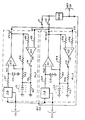
- CK1 indicates the clock signal of a digital signal at input 1
- CK2 indicates the clock signal of a digital signal at input 2
- REF CK indicates the reference clock signal which is generated by a conventional voltage controlled quartz oscillator VCXO and is applied to the inputs of the two identical automatic phase control circuits PLL1 and PLL2, which traversly control the phase of the voltage controlled quartz oscillator VCXO in a similar manner.
- 11 and 12 indicate switches which, according to a predetermined logic, determine the phase latching of the oscillator VCXO to the clock signal of the digital signal at input 1 labeled CK 1 through the phase control circuit PLL1 or the digital signal at input 2 labeled CK 2 through the phase control circuit PLL2.
- ⁇ indicates a conventional phase comparator . circuit which compares the phase of the clock signal of the digital signal at input 1 (CK1) or 2 (CK2) with the phase of the reference clock signal REF CK.
- the signal Vxl indicates the direct voltage, having a magnitude proportional to the phase difference between the two input signals CK1 and REF CK to the phase comparator ⁇ , at the input to the operational amplifier IC3.
- the signal V3 indicates the voltage at the output of the operational amplifier IC3, which is equal to the control voltage VC1 of the voltage controlled quartz oscillator VCXO when the switch Il is closed and simultaneously the switch I2 is open. This same voltage V3 is also applied to a first input of the operational amplifier IC4 of the phase control circuit PLL1 and to a first input of the operational amplifier IC2 of the phase control circuit PLL2.
- the signal Vx2 indicates the direct voltage having a magnitude proportional to the phase difference between the two input signals CK2 and REF CK to the phase comparator ⁇ of phase control circuit PLL2, at the non-inverting input to the operational smplifier IC1.
- the signal Vl indicates the output voltage from the operational amplifier IC1 which is equal to the control voltage of the voltage controlled quartz oscillator VCXO when the switch 12 is closed and simultaneously the switch Il is open. This same voltage Vl is also applied to a second non-inverting input of the operational amplifier IC2 of phase control circuit PLL2 and to a second inverting input of the operational amplifier IC4 of the phase control circuit of PLL1.
- the signal V2 indicates the output voltage from the operational amplifier IC2 of the phase control circuit PLL2; I3 indicates a switch which is closed when the switch 11 is closed and the switch 12 is open.
- the closure of switch 13 makes it possible to apply the signal voltage V2 to the memory circuit of the phase control circuit PLL2 consisting of the resistances R11, R12 and the capacitor C11.
- the resistor R13 is a matching resistor between the output of the memory circuit and a second inverting input of the operational amplifier IC1 of the phase control circuit PLL2.
- the signal V4 indicates the output voltage from the operational amplifier IC4 of phase control circuit PLLl; 14 indicates a switch which is closed when the switch I2 is closed and the switch 11 is open, and under such conditions applies the signal voltage V4 to the memory circuit of the phase control circuit PLL1 consisting of the resistances Rl, R2 and the capacitor C1; R3 designates a matching resistance between the output of the memory circuit and a second inverting input of the operational amplifier IC3 of the phase control circuit PLL1.
- the voltage V3 VC1 besides controlling the phase of the voltage controlled quartz oscillator VCXO, is applied to the input of the operational amplifier IC2 of the phase control circuit PLL2 and provides at its output a voltage V2 which charges the memory circuit consisting of capacitor Cll and resistors Rll and R12 of the phase control circuit PLL2; this provides at the input of operational amplifier IC1 of the phase control circuit PLL2 a negative feedback voltage such as to maintain the output signal voltage V1 from the operational amplifier ICl of the phase control circuit PLL2 at a value equal to VC1, independently of the value of the input signal voltage Vx2.
- Vl Vcl and is maintained at the same value by the charge voltage of the capacitor C11.
- the signal voltage Vl will then tend to reach the new value VC2 equal to the new value of the control voltage of the oscillator VCXO at a rate equal to that of the discharge of the capacitor Cll on R12.
- the discharge time constant for this memory comprised of the capacitor Cl and resistor R2 is given by T ⁇ CR2 and is dimensioned in such a manner that the jitter transient imparted to the signal is within the amplitude and frequency limits predetermined by the international recommendation (recommendation G.703 of CCITT).
- phase control circuit PLL1 operates as described above for phase control circuit PLL2.
- the voltage V1 VC2 besides controlling the phase of the voltage controlled quartz oscillator VCXO, is applied to the input of operational amplifiers IC4 of the phase control circuit PLL1 and determines at its output a signal voltage V4 which charges the memory circuit of the phase control circuit PLL1; this then establishes an the input of operational amplifier IC3 of PLL1 a degenerative voltage such as to maintain the signal voltage V3 at the output from operational amplifier IC3 of PLL1 at a value equal to VC2, independently of the value of the input voltage Vx1.
Landscapes
- Engineering & Computer Science (AREA)
- Computer Networks & Wireless Communication (AREA)
- Signal Processing (AREA)
- Stabilization Of Oscillater, Synchronisation, Frequency Synthesizers (AREA)
- Analogue/Digital Conversion (AREA)
- Synchronisation In Digital Transmission Systems (AREA)
Applications Claiming Priority (2)
| Application Number | Priority Date | Filing Date | Title |
|---|---|---|---|
| US06/654,337 US4600896A (en) | 1984-09-25 | 1984-09-25 | Circuit for limiting jitter transients during switching of phase control signals to an oscillator |
| US654337 | 1984-09-25 |
Publications (3)
| Publication Number | Publication Date |
|---|---|
| EP0175888A2 true EP0175888A2 (de) | 1986-04-02 |
| EP0175888A3 EP0175888A3 (en) | 1987-11-11 |
| EP0175888B1 EP0175888B1 (de) | 1991-06-19 |
Family
ID=24624450
Family Applications (1)
| Application Number | Title | Priority Date | Filing Date |
|---|---|---|---|
| EP85109756A Expired - Lifetime EP0175888B1 (de) | 1984-09-25 | 1985-08-02 | Schaltung zur Begrenzung von momentanen Phasenschwankungen während des Schaltens |
Country Status (8)
| Country | Link |
|---|---|
| US (1) | US4600896A (de) |
| EP (1) | EP0175888B1 (de) |
| JP (1) | JPS6181022A (de) |
| AU (1) | AU587583B2 (de) |
| CA (1) | CA1213946A (de) |
| DE (1) | DE3583268D1 (de) |
| IT (1) | IT1175870B (de) |
| ZA (1) | ZA856787B (de) |
Cited By (4)
| Publication number | Priority date | Publication date | Assignee | Title |
|---|---|---|---|---|
| EP0353616A1 (de) * | 1988-08-02 | 1990-02-07 | Siemens Aktiengesellschaft | Verfahren zur Synchronisation eines Taktes auf störbehaftete Referenztakte |
| EP0517431A1 (de) * | 1991-05-28 | 1992-12-09 | Codex Corporation | Schaltung und Verfahren zum Umschalten zwischen redundanten Takten in einem Phasenregelkreis |
| WO1997020410A1 (en) * | 1995-11-30 | 1997-06-05 | Telefonaktiebolaget Lm Ericsson (Publ) | A method for reducing transients in a clock signal generating system |
| WO1998024185A1 (de) * | 1996-11-26 | 1998-06-04 | Siemens Aktiengesellschaft | Synchronisationseinrichtung einer baugruppe |
Families Citing this family (7)
| Publication number | Priority date | Publication date | Assignee | Title |
|---|---|---|---|---|
| US4600896A (en) * | 1984-09-25 | 1986-07-15 | Gte Communication Systems Corporation | Circuit for limiting jitter transients during switching of phase control signals to an oscillator |
| US4752749A (en) * | 1986-12-22 | 1988-06-21 | Rockwell International Corporation | Fast response tuner |
| JP3208736B2 (ja) * | 1991-11-08 | 2001-09-17 | ソニー株式会社 | Pll回路 |
| DE4408852C1 (de) * | 1994-03-16 | 1994-11-17 | Ant Nachrichtentech | Verfahren zur Bereitstellung eines Rahmentaktes sowie Anordnung und Anwendung |
| KR0177731B1 (ko) * | 1994-09-15 | 1999-05-15 | 정장호 | 망동기용 디지탈 위상동기루프 제어방법 |
| US5986486A (en) * | 1997-11-10 | 1999-11-16 | Adc Telecommunications, Inc. | Circuits and methods for a phase lock loop for synchronous reference clocks |
| US7140952B1 (en) * | 2005-09-22 | 2006-11-28 | Pratt & Whitney Canada Corp. | Oxidation protected blade and method of manufacturing |
Family Cites Families (2)
| Publication number | Priority date | Publication date | Assignee | Title |
|---|---|---|---|---|
| US4511859A (en) * | 1982-08-30 | 1985-04-16 | At&T Bell Laboratories | Apparatus for generating a common output signal as a function of any of a plurality of diverse input signals |
| US4600896A (en) * | 1984-09-25 | 1986-07-15 | Gte Communication Systems Corporation | Circuit for limiting jitter transients during switching of phase control signals to an oscillator |
-
1984
- 1984-09-25 US US06/654,337 patent/US4600896A/en not_active Expired - Fee Related
- 1984-10-19 IT IT23237/84A patent/IT1175870B/it active
-
1985
- 1985-06-14 CA CA000484092A patent/CA1213946A/en not_active Expired
- 1985-08-02 DE DE8585109756T patent/DE3583268D1/de not_active Expired - Lifetime
- 1985-08-02 EP EP85109756A patent/EP0175888B1/de not_active Expired - Lifetime
- 1985-08-29 JP JP60190886A patent/JPS6181022A/ja active Granted
- 1985-09-04 ZA ZA856787A patent/ZA856787B/xx unknown
- 1985-09-24 AU AU47824/85A patent/AU587583B2/en not_active Ceased
Cited By (7)
| Publication number | Priority date | Publication date | Assignee | Title |
|---|---|---|---|---|
| EP0353616A1 (de) * | 1988-08-02 | 1990-02-07 | Siemens Aktiengesellschaft | Verfahren zur Synchronisation eines Taktes auf störbehaftete Referenztakte |
| EP0517431A1 (de) * | 1991-05-28 | 1992-12-09 | Codex Corporation | Schaltung und Verfahren zum Umschalten zwischen redundanten Takten in einem Phasenregelkreis |
| WO1997020410A1 (en) * | 1995-11-30 | 1997-06-05 | Telefonaktiebolaget Lm Ericsson (Publ) | A method for reducing transients in a clock signal generating system |
| AU712876B2 (en) * | 1995-11-30 | 1999-11-18 | Telefonaktiebolaget Lm Ericsson (Publ) | A method for reducing transients in a clock signal generating system |
| US6256360B1 (en) | 1995-11-30 | 2001-07-03 | Telefonaktiebolaget Lm Ericsson (Publ) | Method for reducing transients in a clock signal generating system |
| WO1998024185A1 (de) * | 1996-11-26 | 1998-06-04 | Siemens Aktiengesellschaft | Synchronisationseinrichtung einer baugruppe |
| US6147562A (en) * | 1996-11-26 | 2000-11-14 | Siemens Aktiengesellschaft | Apparatus for synchronizing master and slave processors |
Also Published As
| Publication number | Publication date |
|---|---|
| JPS6181022A (ja) | 1986-04-24 |
| IT1175870B (it) | 1987-07-15 |
| DE3583268D1 (de) | 1991-07-25 |
| CA1213946A (en) | 1986-11-12 |
| IT8423237A0 (it) | 1984-10-19 |
| JPH0325102B2 (de) | 1991-04-05 |
| ZA856787B (en) | 1986-05-28 |
| EP0175888B1 (de) | 1991-06-19 |
| EP0175888A3 (en) | 1987-11-11 |
| AU4782485A (en) | 1986-04-10 |
| AU587583B2 (en) | 1989-08-24 |
| IT8423237A1 (it) | 1986-04-19 |
| US4600896A (en) | 1986-07-15 |
Similar Documents
| Publication | Publication Date | Title |
|---|---|---|
| EP0116559B1 (de) | Zeitsteuerverzögerungsausgleichsschaltung | |
| EP0652642B1 (de) | Phasenregelschleife mit Überbrückungsmodus | |
| EP0175888A2 (de) | Schaltung zur Begrenzung von momentanen Phasenschwankungen während des Schaltens | |
| US5276408A (en) | PLL frequency synthesizer capable of changing an output frequency at a high speed | |
| GB2180708A (en) | Phase-comparator lock-detect circuit for a frequency synthesiser | |
| US5268654A (en) | Phase locked loop clock changeover apparatus in which the VCO is set to an initial value | |
| JPS6342971B2 (de) | ||
| US5416691A (en) | Charge pump circuit | |
| US6249160B1 (en) | Clock reproduction and identification apparatus | |
| US5329252A (en) | Slew-rate limited voltage controlled oscillator control voltage clamp circuit | |
| EP0098653B1 (de) | Taktsignalregenerator mit hoher Stabilität | |
| JPH10501108A (ja) | 位相固定ループを制御する方法および位相固定ループ | |
| GB1574961A (en) | Detectors for tones | |
| JP2523403B2 (ja) | 電圧測定装置 | |
| CA2152181A1 (en) | Apparatus and Method for Enabling Elements of a Phase Locked Loop | |
| US4937538A (en) | Circuit arrangement for synchronizing an oscillator | |
| JPH047911A (ja) | 位相同期発振回路 | |
| JPH0786931A (ja) | 周波数シンセサイザ | |
| JPS6297428A (ja) | Pll回路 | |
| CA2108207C (en) | Frequency stabilizer for use in phase-shift keying radio communications system | |
| CN85106845A (zh) | 用于在交换期间限制暂态抖动的电路 | |
| EP0868783B1 (de) | Verfahren und schaltung zur aufrechterhaltung des synchronisierten zustandes in einem digitalen phasenregelkreis | |
| JPS6024733A (ja) | 自動周波数制御回路 | |
| JPH0290811A (ja) | 周波数位相同期回路 | |
| JPH0220121A (ja) | 位相同期ループ回路 |
Legal Events
| Date | Code | Title | Description |
|---|---|---|---|
| PUAI | Public reference made under article 153(3) epc to a published international application that has entered the european phase |
Free format text: ORIGINAL CODE: 0009012 |
|
| AK | Designated contracting states |
Kind code of ref document: A2 Designated state(s): BE DE FR GB NL |
|
| PUAL | Search report despatched |
Free format text: ORIGINAL CODE: 0009013 |
|
| AK | Designated contracting states |
Kind code of ref document: A3 Designated state(s): BE DE FR GB NL |
|
| 17P | Request for examination filed |
Effective date: 19880302 |
|
| RAP1 | Party data changed (applicant data changed or rights of an application transferred) |
Owner name: SIEMENS TELECOMUNICAZIONI S.P.A. |
|
| 17Q | First examination report despatched |
Effective date: 19891218 |
|
| GRAA | (expected) grant |
Free format text: ORIGINAL CODE: 0009210 |
|
| AK | Designated contracting states |
Kind code of ref document: B1 Designated state(s): BE DE FR GB NL |
|
| REF | Corresponds to: |
Ref document number: 3583268 Country of ref document: DE Date of ref document: 19910725 |
|
| ET | Fr: translation filed | ||
| PLBE | No opposition filed within time limit |
Free format text: ORIGINAL CODE: 0009261 |
|
| STAA | Information on the status of an ep patent application or granted ep patent |
Free format text: STATUS: NO OPPOSITION FILED WITHIN TIME LIMIT |
|
| 26N | No opposition filed | ||
| PGFP | Annual fee paid to national office [announced via postgrant information from national office to epo] |
Ref country code: GB Payment date: 19960718 Year of fee payment: 12 |
|
| PGFP | Annual fee paid to national office [announced via postgrant information from national office to epo] |
Ref country code: BE Payment date: 19960819 Year of fee payment: 12 |
|
| PGFP | Annual fee paid to national office [announced via postgrant information from national office to epo] |
Ref country code: NL Payment date: 19960821 Year of fee payment: 12 |
|
| PGFP | Annual fee paid to national office [announced via postgrant information from national office to epo] |
Ref country code: FR Payment date: 19960830 Year of fee payment: 12 |
|
| PGFP | Annual fee paid to national office [announced via postgrant information from national office to epo] |
Ref country code: DE Payment date: 19961022 Year of fee payment: 12 |
|
| PG25 | Lapsed in a contracting state [announced via postgrant information from national office to epo] |
Ref country code: GB Free format text: LAPSE BECAUSE OF NON-PAYMENT OF DUE FEES Effective date: 19970802 |
|
| PG25 | Lapsed in a contracting state [announced via postgrant information from national office to epo] |
Ref country code: BE Free format text: LAPSE BECAUSE OF NON-PAYMENT OF DUE FEES Effective date: 19970831 |
|
| BERE | Be: lapsed |
Owner name: SIEMENS TELECOMUNICAZIONI S.P.A. Effective date: 19970831 |
|
| PG25 | Lapsed in a contracting state [announced via postgrant information from national office to epo] |
Ref country code: NL Free format text: LAPSE BECAUSE OF NON-PAYMENT OF DUE FEES Effective date: 19980301 |
|
| GBPC | Gb: european patent ceased through non-payment of renewal fee |
Effective date: 19970802 |
|
| PG25 | Lapsed in a contracting state [announced via postgrant information from national office to epo] |
Ref country code: FR Free format text: LAPSE BECAUSE OF NON-PAYMENT OF DUE FEES Effective date: 19980430 |
|
| PG25 | Lapsed in a contracting state [announced via postgrant information from national office to epo] |
Ref country code: DE Free format text: LAPSE BECAUSE OF NON-PAYMENT OF DUE FEES Effective date: 19980501 |
|
| NLV4 | Nl: lapsed or anulled due to non-payment of the annual fee |
Effective date: 19980301 |
|
| REG | Reference to a national code |
Ref country code: FR Ref legal event code: ST |