EP0176184A1 - Circuit de changement de phase - Google Patents
Circuit de changement de phase Download PDFInfo
- Publication number
- EP0176184A1 EP0176184A1 EP85305296A EP85305296A EP0176184A1 EP 0176184 A1 EP0176184 A1 EP 0176184A1 EP 85305296 A EP85305296 A EP 85305296A EP 85305296 A EP85305296 A EP 85305296A EP 0176184 A1 EP0176184 A1 EP 0176184A1
- Authority
- EP
- European Patent Office
- Prior art keywords
- circuit
- ecl
- emitter
- control
- phase changing
- Prior art date
- Legal status (The legal status is an assumption and is not a legal conclusion. Google has not performed a legal analysis and makes no representation as to the accuracy of the status listed.)
- Granted
Links
Images


Classifications
-
- H—ELECTRICITY
- H03—ELECTRONIC CIRCUITRY
- H03K—PULSE TECHNIQUE
- H03K19/00—Logic circuits, i.e. having at least two inputs acting on one output; Inverting circuits
- H03K19/02—Logic circuits, i.e. having at least two inputs acting on one output; Inverting circuits using specified components
- H03K19/08—Logic circuits, i.e. having at least two inputs acting on one output; Inverting circuits using specified components using semiconductor devices
-
- H—ELECTRICITY
- H03—ELECTRONIC CIRCUITRY
- H03K—PULSE TECHNIQUE
- H03K5/00—Manipulating of pulses not covered by one of the other main groups of this subclass
- H03K5/13—Arrangements having a single output and transforming input signals into pulses delivered at desired time intervals
- H03K5/131—Digitally controlled
-
- H—ELECTRICITY
- H03—ELECTRONIC CIRCUITRY
- H03K—PULSE TECHNIQUE
- H03K19/00—Logic circuits, i.e. having at least two inputs acting on one output; Inverting circuits
- H03K19/003—Modifications for increasing the reliability for protection
- H03K19/00323—Delay compensation
-
- H—ELECTRICITY
- H03—ELECTRONIC CIRCUITRY
- H03K—PULSE TECHNIQUE
- H03K5/00—Manipulating of pulses not covered by one of the other main groups of this subclass
- H03K2005/00013—Delay, i.e. output pulse is delayed after input pulse and pulse length of output pulse is dependent on pulse length of input pulse
- H03K2005/00078—Fixed delay
-
- H—ELECTRICITY
- H03—ELECTRONIC CIRCUITRY
- H03K—PULSE TECHNIQUE
- H03K5/00—Manipulating of pulses not covered by one of the other main groups of this subclass
- H03K2005/00013—Delay, i.e. output pulse is delayed after input pulse and pulse length of output pulse is dependent on pulse length of input pulse
- H03K2005/0015—Layout of the delay element
- H03K2005/00163—Layout of the delay element using bipolar transistors
- H03K2005/00176—Layout of the delay element using bipolar transistors using differential stages
-
- H—ELECTRICITY
- H03—ELECTRONIC CIRCUITRY
- H03K—PULSE TECHNIQUE
- H03K5/00—Manipulating of pulses not covered by one of the other main groups of this subclass
- H03K2005/00013—Delay, i.e. output pulse is delayed after input pulse and pulse length of output pulse is dependent on pulse length of input pulse
- H03K2005/0015—Layout of the delay element
- H03K2005/00163—Layout of the delay element using bipolar transistors
- H03K2005/00182—Layout of the delay element using bipolar transistors using constant current sources
Definitions
- the present invention relates to a phase changing circuit in a logic circuit.
- clock signals having desired phases must be distributed to latches in the processor.
- the desired clocks are obtained by making use, in a clock distribution circuit, of a delay line with delay values obtained by taps or discrete wires (pair wires, fine wires, coaxial cables, etc.) with delay values adjustable by changing the length.
- An / of the present invention can provide a phase changing circuit, in a logic circuit, which can delay the phase of a transmission signal without occupying extensive space.
- An embodiment of the present invention can provide a phase changing circuit, in a logic circuit, which can adjust the phase of a transmission signal by using a gate of an LSI.
- a phase changing circuit in a logic circuit including an ECL circuit which has a plurality of emitter-output circuits, including a first emitter output circuit in the ECL circuit used as a normal output portion and a second emitter output circuit in the ECL circuit connected by a first capacitor.
- the second emitter output circuit is connected to an emitter output circuit of a first control ECL circuit provided independently of the ECL circuit.
- An electric potential of the second emitter output circuit is turned on or off by changing a control input of the first control ECL circuit.
- the signal transmission from an input to the normal output portion of the ECL circuit is delayed when the emitter potential of the second emitter circuit is on.
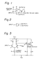
- FIG. 1 is a block diagram of an embodiment of the phase changing circuit of the present invention.
- 11 designates an ECL gate (signal gate) having one input and two OR outputs, 12 a control gate having one input and one OR output, 13 an additional capacitor 14 an input portion, 15 an output portion to be used (signal output portion) and 16 a control input portion.
- ECL gate signal gate
- 12 a control gate having one input and one OR output
- 13 an additional capacitor 14 an input portion
- 15 an output portion to be used (signal output portion)
- 16 a control input portion.
- Fig. 2 is a symbol diagram of an ECL gate having one input and two OR outputs shown in Fig. 1
- Fig. 3 is an example of an internal construction of the ECL gate shown in Fig. 2.
- 1 to 4 are transistors
- 5 is a current source
- 6 to 9 are resistors
- 10 is a capacitance (C BE ) between a base and an emitter of the transistor 4
- V CC and V EE are power sources
- V REF is a reference power source.
- the signal transmission delay time from the input to the output in question can be adjusted.
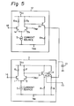
- FIG. 5 is a detailed circuit diagram of the phase changing circuit shown in Fig. 1.
- the gate 12 in Fig. 5 has the same construction as the ECL gate 11 except that an output emitter circuit portion to be used as a employed. normal output is not /
- the control input portion 16 when the control input portion 16 is a low level compared with the reference voltage V REF , the current flows via the transistor 2a, and the collector of the transistor 2a becomes low level, so that the emitter of the transistor 3a is placed at the low level.
- a gate having three/OR outputs may be used.
- 20 is a gate having one input and three OR outputs
- 21 and 22 are a control gate each having one input and one OR output respectively
- 23 and 24 are additional capacitors (C 1 , C 2 ).
- the delay time can be controlled by the control signals 1 and 2 when the values of C 1 , C2 are changed.
- Fig. 7 25 is an ECL gate having one input and two NOR outputs, 26 is a control gate having one input and one OR output, and 27 is an additional capacitor.
- Fig. 8 is a time chart of the embodiment shown in Fig. 7.
- Figure 9 shows two of the circuits shown in Fig. 7 connected in series so as to delay the input pulse.
- Figures 10A, 10B, and 10C show waveforms at the portions (a), (b), and (c) of the circuit in Fig. 9.
- Figure 10A is a waveform of the input pulse.
- Figure 10B is a waveform of the output of the gate 25a, that is, the input of.the gate 25b.
- the falling portion of the (input) pulse is delayed by ATpd when the control input level is low.
- Figure 10C is a waveform of the output pulse of the gate 25b.
- the rising portion of the input pulse is delayed by ATpd.
- the phase of a signal in the internal circuit of an LSI, etc. can be easily adjusted and the advantages of miniaturization of the apparatus, etc. can be obtained.
- Fig. 6 shows a gate having three OR outputs, and two control gates
- Each of the OR outputs2 ... n of the gate in question may have the same form as the output portion consisting of transistor 4, capacitance 10 and resistor 9 shown in Figure 5.
- a respective additional capacitor C1, C2, ... C(N-1) may be provided.
Landscapes
- Physics & Mathematics (AREA)
- Engineering & Computer Science (AREA)
- Computer Hardware Design (AREA)
- Computing Systems (AREA)
- General Engineering & Computer Science (AREA)
- Mathematical Physics (AREA)
- Nonlinear Science (AREA)
- Power Engineering (AREA)
- Pulse Circuits (AREA)
- Networks Using Active Elements (AREA)
- Logic Circuits (AREA)
Applications Claiming Priority (2)
| Application Number | Priority Date | Filing Date | Title |
|---|---|---|---|
| JP15820884A JPS6135609A (ja) | 1984-07-28 | 1984-07-28 | 位相可変回路 |
| JP158208/84 | 1984-07-28 |
Publications (2)
| Publication Number | Publication Date |
|---|---|
| EP0176184A1 true EP0176184A1 (fr) | 1986-04-02 |
| EP0176184B1 EP0176184B1 (fr) | 1989-05-03 |
Family
ID=15666641
Family Applications (1)
| Application Number | Title | Priority Date | Filing Date |
|---|---|---|---|
| EP85305296A Expired EP0176184B1 (fr) | 1984-07-28 | 1985-07-25 | Circuit de changement de phase |
Country Status (9)
| Country | Link |
|---|---|
| US (1) | US4717843A (fr) |
| EP (1) | EP0176184B1 (fr) |
| JP (1) | JPS6135609A (fr) |
| KR (1) | KR890005233B1 (fr) |
| AU (1) | AU560278B2 (fr) |
| BR (1) | BR8503564A (fr) |
| CA (1) | CA1250349A (fr) |
| DE (1) | DE3570025D1 (fr) |
| ES (1) | ES8609848A1 (fr) |
Cited By (2)
| Publication number | Priority date | Publication date | Assignee | Title |
|---|---|---|---|---|
| DE3742075A1 (de) * | 1986-12-12 | 1988-06-23 | Grass Valley Group | Vorrichtung zur kompensation von schaltverzoegerungen |
| FR2826803A1 (fr) * | 2001-06-27 | 2003-01-03 | Mitsubishi Electric Corp | Dispositif a semiconducteur |
Families Citing this family (7)
| Publication number | Priority date | Publication date | Assignee | Title |
|---|---|---|---|---|
| JPS62250713A (ja) * | 1986-04-23 | 1987-10-31 | Fujitsu Ltd | 可変遅延回路 |
| US5548236A (en) * | 1987-02-20 | 1996-08-20 | Pixel Instruments | Phase shifting apparatus and method with frequency multiplication |
| JPS63238713A (ja) * | 1987-03-26 | 1988-10-04 | Oki Electric Ind Co Ltd | 遅延回路 |
| US4812687A (en) * | 1988-07-13 | 1989-03-14 | International Business Machines Corporation | Dual direction integrating delay circuit |
| US5343348A (en) * | 1991-04-03 | 1994-08-30 | Victor Company Of Japan, Ltd. | Actuator for displacing a magnetic head |
| JP2594062Y2 (ja) * | 1991-12-05 | 1999-04-19 | 株式会社アドバンテスト | 微小可変遅延回路 |
| US5376849A (en) * | 1992-12-04 | 1994-12-27 | International Business Machines Corporation | High resolution programmable pulse generator employing controllable delay |
Family Cites Families (5)
| Publication number | Priority date | Publication date | Assignee | Title |
|---|---|---|---|---|
| JPS5382142A (en) * | 1976-12-27 | 1978-07-20 | Fujitsu Ltd | Clock distributing system |
| JPS5391443A (en) * | 1977-01-20 | 1978-08-11 | Kubota Ltd | Hot-water controlling apparatus for hot-water tank |
| JPS56156026A (en) * | 1980-05-02 | 1981-12-02 | Hitachi Ltd | Composite logical circuit |
| JPS58108824A (ja) * | 1981-12-23 | 1983-06-29 | Fujitsu Ltd | Ecl型遅延回路 |
| JPS594231A (ja) * | 1982-06-30 | 1984-01-11 | Hitachi Ltd | 高速論理回路 |
-
1984
- 1984-07-28 JP JP15820884A patent/JPS6135609A/ja active Granted
-
1985
- 1985-07-18 CA CA000487051A patent/CA1250349A/fr not_active Expired
- 1985-07-24 US US06/758,391 patent/US4717843A/en not_active Expired - Fee Related
- 1985-07-24 KR KR1019850005294A patent/KR890005233B1/ko not_active Expired
- 1985-07-24 AU AU45310/85A patent/AU560278B2/en not_active Ceased
- 1985-07-25 EP EP85305296A patent/EP0176184B1/fr not_active Expired
- 1985-07-25 DE DE8585305296T patent/DE3570025D1/de not_active Expired
- 1985-07-26 BR BR8503564A patent/BR8503564A/pt not_active IP Right Cessation
- 1985-07-26 ES ES545591A patent/ES8609848A1/es not_active Expired
Non-Patent Citations (4)
| Title |
|---|
| IBM TECHNICAL DISCLOSURE BULLETIN, vol. 16, no. 11, April 1974, pages 3498-3500; P.T. MARINO "Variable delay pulse circuits" * |
| IBM TECHNICAL DISCLOSURE BULLETIN, vol. 21, no. 4, September 1978, pages 1582,1583; R.P. CHRISFIELD et al.: "Continuous integrated circuit delay line" * |
| IBM TECHNICAL DISCLOSURE BULLETIN, vol. 22, no. 2, July 1979, pages 518, 519; L.M. ARZUBI "Encoded variable delay for driver circuits" * |
| PATENT ABSTRACTS OF JAPAN, vol. 7, no. 218 (E-200)[1363], 28th September 1983; & JP-A-58 108 824 (FUJITSU K.K.) 29-06-1983 * |
Cited By (5)
| Publication number | Priority date | Publication date | Assignee | Title |
|---|---|---|---|---|
| DE3742075A1 (de) * | 1986-12-12 | 1988-06-23 | Grass Valley Group | Vorrichtung zur kompensation von schaltverzoegerungen |
| FR2826803A1 (fr) * | 2001-06-27 | 2003-01-03 | Mitsubishi Electric Corp | Dispositif a semiconducteur |
| FR2827441A1 (fr) * | 2001-06-27 | 2003-01-17 | Mitsubishi Electric Corp | Dispositif a semiconducteur |
| US7132868B2 (en) | 2001-06-27 | 2006-11-07 | Mitsubishi Denki Kabushiki Kaisha | Semiconductor device |
| US7274223B2 (en) | 2001-06-27 | 2007-09-25 | Mitsubishi Denki Kabushiki Kaisha | Semiconductor device |
Also Published As
| Publication number | Publication date |
|---|---|
| ES545591A0 (es) | 1986-09-01 |
| BR8503564A (pt) | 1986-04-22 |
| AU4531085A (en) | 1986-02-06 |
| JPS6135609A (ja) | 1986-02-20 |
| KR890005233B1 (ko) | 1989-12-18 |
| DE3570025D1 (en) | 1989-06-08 |
| US4717843A (en) | 1988-01-05 |
| ES8609848A1 (es) | 1986-09-01 |
| EP0176184B1 (fr) | 1989-05-03 |
| JPH0220171B2 (fr) | 1990-05-08 |
| CA1250349A (fr) | 1989-02-21 |
| KR860001643A (ko) | 1986-03-20 |
| AU560278B2 (en) | 1987-04-02 |
Similar Documents
| Publication | Publication Date | Title |
|---|---|---|
| KR0136775B1 (ko) | 스위칭 유도 잡음을 감소시키는 출력 버퍼 | |
| KR100228756B1 (ko) | 점진적 턴-온 특성의 cmos 구동기 | |
| EP0133359A2 (fr) | Dispositif pour synchroniser un ensemble de puces | |
| CA1257342A (fr) | Circuit logique integre incorporant un module generateur de signaux annulant le bruit de commutation | |
| JPS62219813A (ja) | デジタル信号用mosfet集積遅延回路 | |
| EP0647025A1 (fr) | Circuit de délai | |
| EP0176184B1 (fr) | Circuit de changement de phase | |
| KR910009083B1 (ko) | 반도체장치의 출력회로 | |
| US6380777B1 (en) | Output driver having controlled slew rate | |
| US5684424A (en) | Pulse skew control | |
| GB2214019A (en) | A distributed precharge wire-or bus | |
| EP0463641B1 (fr) | Système de distribution de signaux d'horloge | |
| US5321320A (en) | ECL driver with adjustable rise and fall times, and method therefor | |
| US5506521A (en) | ECL driver with adjustable rise and fall times, and method therefor | |
| US4967104A (en) | Circuit for increasing the output impedance of an amplifier | |
| EP0219604A2 (fr) | Appareil et méthode de production de signaux en relation de phase avec un signal d'horloge | |
| JPS6331214A (ja) | 可変遅延回路 | |
| JPH11135920A (ja) | プリント配線板およびクロックスキュー調整方法 | |
| JP2808754B2 (ja) | ゲートアレイ型集積回路 | |
| JPS6139650A (ja) | クロツク位相微調回路 | |
| KR19980083401A (ko) | 반도체 장치의 입/출력 버퍼 | |
| JPH0754895B2 (ja) | 可変遅延回路 | |
| JPS6139651A (ja) | クロツク位相微調回路 | |
| JPH04268808A (ja) | ラッチ回路 | |
| Luschnig et al. | Circuit Technique for Ultra Fast D/A Converters |
Legal Events
| Date | Code | Title | Description |
|---|---|---|---|
| PUAI | Public reference made under article 153(3) epc to a published international application that has entered the european phase |
Free format text: ORIGINAL CODE: 0009012 |
|
| AK | Designated contracting states |
Kind code of ref document: A1 Designated state(s): CH DE FR GB IT LI NL SE |
|
| 17P | Request for examination filed |
Effective date: 19860507 |
|
| 17Q | First examination report despatched |
Effective date: 19880802 |
|
| GRAA | (expected) grant |
Free format text: ORIGINAL CODE: 0009210 |
|
| AK | Designated contracting states |
Kind code of ref document: B1 Designated state(s): CH DE FR GB IT LI NL SE |
|
| REF | Corresponds to: |
Ref document number: 3570025 Country of ref document: DE Date of ref document: 19890608 |
|
| ET | Fr: translation filed | ||
| ITF | It: translation for a ep patent filed | ||
| PLBE | No opposition filed within time limit |
Free format text: ORIGINAL CODE: 0009261 |
|
| STAA | Information on the status of an ep patent application or granted ep patent |
Free format text: STATUS: NO OPPOSITION FILED WITHIN TIME LIMIT |
|
| 26N | No opposition filed | ||
| ITTA | It: last paid annual fee | ||
| EAL | Se: european patent in force in sweden |
Ref document number: 85305296.7 |
|
| PGFP | Annual fee paid to national office [announced via postgrant information from national office to epo] |
Ref country code: SE Payment date: 19980707 Year of fee payment: 14 |
|
| PGFP | Annual fee paid to national office [announced via postgrant information from national office to epo] |
Ref country code: FR Payment date: 19980709 Year of fee payment: 14 |
|
| PGFP | Annual fee paid to national office [announced via postgrant information from national office to epo] |
Ref country code: GB Payment date: 19980716 Year of fee payment: 14 |
|
| PGFP | Annual fee paid to national office [announced via postgrant information from national office to epo] |
Ref country code: NL Payment date: 19980728 Year of fee payment: 14 |
|
| PGFP | Annual fee paid to national office [announced via postgrant information from national office to epo] |
Ref country code: DE Payment date: 19980803 Year of fee payment: 14 |
|
| PGFP | Annual fee paid to national office [announced via postgrant information from national office to epo] |
Ref country code: CH Payment date: 19980806 Year of fee payment: 14 |
|
| PG25 | Lapsed in a contracting state [announced via postgrant information from national office to epo] |
Ref country code: GB Free format text: LAPSE BECAUSE OF NON-PAYMENT OF DUE FEES Effective date: 19990725 |
|
| PG25 | Lapsed in a contracting state [announced via postgrant information from national office to epo] |
Ref country code: SE Free format text: THE PATENT HAS BEEN ANNULLED BY A DECISION OF A NATIONAL AUTHORITY Effective date: 19990726 |
|
| PG25 | Lapsed in a contracting state [announced via postgrant information from national office to epo] |
Ref country code: LI Free format text: LAPSE BECAUSE OF NON-PAYMENT OF DUE FEES Effective date: 19990731 Ref country code: FR Free format text: THE PATENT HAS BEEN ANNULLED BY A DECISION OF A NATIONAL AUTHORITY Effective date: 19990731 Ref country code: CH Free format text: LAPSE BECAUSE OF NON-PAYMENT OF DUE FEES Effective date: 19990731 |
|
| PG25 | Lapsed in a contracting state [announced via postgrant information from national office to epo] |
Ref country code: NL Free format text: LAPSE BECAUSE OF NON-PAYMENT OF DUE FEES Effective date: 20000201 |
|
| GBPC | Gb: european patent ceased through non-payment of renewal fee |
Effective date: 19990725 |
|
| REG | Reference to a national code |
Ref country code: CH Ref legal event code: PL |
|
| EUG | Se: european patent has lapsed |
Ref document number: 85305296.7 |
|
| NLV4 | Nl: lapsed or anulled due to non-payment of the annual fee |
Effective date: 20000201 |
|
| PG25 | Lapsed in a contracting state [announced via postgrant information from national office to epo] |
Ref country code: DE Free format text: LAPSE BECAUSE OF NON-PAYMENT OF DUE FEES Effective date: 20000503 |
|
| REG | Reference to a national code |
Ref country code: FR Ref legal event code: ST |