EP0176203A2 - Circuit de commande de rafraîchissement automatique pour une mémoire semi-conductrice dynamique - Google Patents
Circuit de commande de rafraîchissement automatique pour une mémoire semi-conductrice dynamique Download PDFInfo
- Publication number
- EP0176203A2 EP0176203A2 EP85305697A EP85305697A EP0176203A2 EP 0176203 A2 EP0176203 A2 EP 0176203A2 EP 85305697 A EP85305697 A EP 85305697A EP 85305697 A EP85305697 A EP 85305697A EP 0176203 A2 EP0176203 A2 EP 0176203A2
- Authority
- EP
- European Patent Office
- Prior art keywords
- refresh
- capacitor
- circuit
- control circuit
- inverter
- Prior art date
- Legal status (The legal status is an assumption and is not a legal conclusion. Google has not performed a legal analysis and makes no representation as to the accuracy of the status listed.)
- Granted
Links
- 239000004065 semiconductor Substances 0.000 title claims description 7
- 239000003990 capacitor Substances 0.000 claims description 41
- 238000012544 monitoring process Methods 0.000 claims description 5
- 230000004044 response Effects 0.000 claims description 4
- 238000012546 transfer Methods 0.000 description 8
- 230000007423 decrease Effects 0.000 description 4
- 238000010586 diagram Methods 0.000 description 3
- 230000010355 oscillation Effects 0.000 description 2
- 239000004020 conductor Substances 0.000 description 1
- 230000001419 dependent effect Effects 0.000 description 1
- 238000013461 design Methods 0.000 description 1
- 238000011982 device technology Methods 0.000 description 1
- 239000012535 impurity Substances 0.000 description 1
- 238000004519 manufacturing process Methods 0.000 description 1
- 238000000034 method Methods 0.000 description 1
- 229910021420 polycrystalline silicon Inorganic materials 0.000 description 1
- 229920005591 polysilicon Polymers 0.000 description 1
- 238000004088 simulation Methods 0.000 description 1
Images
Classifications
-
- G—PHYSICS
- G11—INFORMATION STORAGE
- G11C—STATIC STORES
- G11C11/00—Digital stores characterised by the use of particular electric or magnetic storage elements; Storage elements therefor
- G11C11/21—Digital stores characterised by the use of particular electric or magnetic storage elements; Storage elements therefor using electric elements
- G11C11/34—Digital stores characterised by the use of particular electric or magnetic storage elements; Storage elements therefor using electric elements using semiconductor devices
- G11C11/40—Digital stores characterised by the use of particular electric or magnetic storage elements; Storage elements therefor using electric elements using semiconductor devices using transistors
- G11C11/401—Digital stores characterised by the use of particular electric or magnetic storage elements; Storage elements therefor using electric elements using semiconductor devices using transistors forming cells needing refreshing or charge regeneration, i.e. dynamic cells
- G11C11/406—Management or control of the refreshing or charge-regeneration cycles
Definitions
- This invention relates to a self-refresh control circuit of a semiconductor memory device, particularly a Dynamic Random Access Memory device (DRAM).
- DRAM Dynamic Random Access Memory
- Recent advances in semiconductor dynamic memory device technology enable a self-refresh circuit to be incorporated on a single chip having memory cells, which can perform a self-refresh operation automatically by itself and eliminate the need for timing or address control circuits outside the chip.
- this type of self-refresh circuit includes an oscillator and refresh address counter, which are provided for designating the address of memory cells during the refresh operation when the memory cells are on "standby" operation or not in the read or write operation.
- the oscillator circuit which determines the frequency of refresh operation, comprises MOS-FETS.
- MOS-FETS the speed of operation of a MOS-FET becomes lower as temperature increases.
- the frequency of the oscillator decreases at high temperatures.
- the current leakage of a memory cell approximately doubles when the temperature rises by 10°. Accordingly, the frequency of the oscillator is set high enough so as to operate satisfactorily even at high temperatures. The result is that the frequency of the refresh operation at low temperatures is higher than required.
- the frequency is set about 100 times as high as is actually needed in ordinary temperature.
- the refresh operation involves a certain power consumption.
- 256K DRAM consumes several miliamperes of current on standby operation. Because of this high power consumption, it is very difficult to operate DRAMS using a dry battery as a power source.
- Japanese Laid Open patent 59-56291 provides a memory device which automatically controls the frequency of the refresh operation to be as much as needed so as to reduce the power consumption.
- This refresh control circuit comprises two leakage current monitor capacitors, each of which is precharged to some respective predetermined level, and a voltage comparator circuit for detecting the voltage difference between the two capacitors and causing a refresh operation when required in accordance with the voltage difference.
- this refresh control circuit still has the following problems. First, it is very difficult to design the characteristics of two capacitors such as current leakage time or initially charged voltages to provide a proper simulation of memory cells because the leak current monitoring system does not detect the current leakage time of the capacitor itself but the difference of two capacitors. Therefore, unless the characteristics are arranged appropriately, it is not necessarily possible to monitor the current leakage time of memory cells exactly. Second, the comparator circuit still wastes power because a current flows throughout the circuit. This reduces the primary advantages of this circuit.
- the present invention therefore seeks to provide a self-refresh control circuit for dynamic semiconductor memory devices in which the power consumption of the memory device on standby operation can be minimised.
- the present invention also seeks to provide a self-refresh control circuit in which the power consumption of the control circuit itself is small.
- the present invention further seeks to provide a self-refresh control circuit by means of which the stored information of DRAM can be maintained by a dry battery voltage source.
- a refresh control circuit for a dynamic semiconductor memory device having a plurality of memory cells comprising:
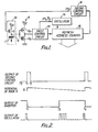
- the automatic self-refresh control circuit for a dynamic memory shown in Figure 1 includes one capacitor serially connected to one transfer gate.
- the circuit comprises leak current monitor circuit 10 having a capacitor C serially connected to a transfer gate Q between a voltage source Vp D and a constant voltage terminal (in this case, an earth terminal).
- CMOS inverter circuit 11 connected to the capacitor C has a N-type MOS transistor Q N and P-type MOS transistor Qp whose conductance is larger than Q N .
- the threshold voltage Vth of this circuit is designed to be larger than I V DD by a predetermined level according to the difference in conductance of the transistors Qp and Q N .
- a first control circuit 13 receives the output signal of the CMOS inverter circuit and waveshapes it as an output signal applied to a self-excited oscillator 14 which is thus set into oscillation by the signal.
- a refresh address counter 15 is put into a reset mode by receiving the output signal from the control circuit 13 and counts the output signal from the oscillator 14 to make a refresh address signal which is sent to a row decoder which drives a word line selectively.
- a second control circuit 16 receives an overflow signal from the counter which generates a pulse output having a constant width when the count exceeds the number of all word lines. This pulse signal puts the transfer gate into the ON state and charges the capacitor C.
- the output signal of the second control circuit 16 puts the transfer gate Q into the ON state in the period tl to t2 and charges the capacitor C.
- the connecting point of Q and C, i.e. the node N, is thus charged up to "1" level.
- the potential level of this node N is intended to represent the leakage of a memory cell of the dynamic memory. That is to say, if the leakage current of the memory cell is larger, the potential level of the node N should fall to zero volts more quickly and if the leakage current is smaller, it should fall more slowly.
- the output signal of the inverter circuit 11 changes to "1" level from "0" level and this signal is shaped by the first control circuit 13.
- the output signal of the control circuit 13 puts the refresh address counter 15 into the reset mode and starts the oscillator 14.
- the oscillator 14 begins to generate pulse signals, which are counted by the counter 15 in order to produce the refresh addresses.
- an overflow signal is applied to the second control circuit 16 WhICh generates a further pulse signal having a constant width to drive the transfer gate Q and charge the capacitor C again.
- the time during which the potential level of the node N in the leak current monitor circuit 10 changes to the Vth level, which is the threshold voltage of the CMOS inverter circuit 11, from the precharged level, is shorter than the time which would be taken for the information stored in a capacitor of memory cell to be lost.
- the Vth of the CMOS inverter circuit 11 is designed to be higher than t V DD .
- the refresh operation is performed in a short period if the leakage current of memory cell is large, and in a longer period if the leakage current is small. Accordingly, it is possible to control the period of the refresh operation to the most desirable value by monitoring the leakage current of a memory cell.
- the frequency can be set to about 1/100 of that of a conventional circuit. In this way the power consumption at a stand-by state can be minimised.
- no direct current path needs to be provided through the CMOS inverter circuit 11 for monitoring the leakage current and the power consumption of the circuit is small, so it is possible to construct a DRAM which can operate with a dry battery as a power source.
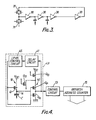
- FIG. 3 shows one embodiment of the oscillator 14.
- This circuit comprises a plurality of CMOS inverter circuits connected in a ring and transfer gates 31, 32 having inputs receiving complimentary control signals from the first control circuit 13 respectively. These transfer gates 31, 32 control whether the circuit starts to oscillate or not.
- the embodiment of Figure 1 shows an example of an intermittent type refresh circuit.
- This circuit monitors the change of potential of the capacitor C and starts the oscillator 14 when the voltage decreases under some predetermined level. Then the memory cells are all refreshed one after another. That is to say, the refresh operation is performed intermittently.
- FIG. 4 An alternative embodiment of this invention shown in Figure 4 represents a distributed type refresh circuit.
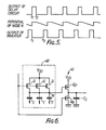
- This circuit employs a precharge-discharge type inverter circuit 40 which receives an output signal from the leakage monitor circuit 10 and generates a signal to the control terminal of the transfer gate Q of the leakage monitor circuit 10 through a delay circuit 41 and a level control circuit 45 so as to make a closed loop circuit which operates as an oscillator. The operation of this circuit will be described with reference to Figure 5.
- the leakage of the capacitor C corresponds to that of a memory cell.
- the threshold voltage of the inverter circuit 40 By setting the threshold voltage of the inverter circuit 40 to be a little higher, it is possible to establish the frequency of the oscillator at a desired value for the actual memory cells.
- the output signal of the inverter 40 is shaped by the control circuit 13 and counted by the refresh address counter 15.
- the inverter 40 includes additional transistors Q10 and Q11, the circuit certainly operates as an inverter. These transistors Q10 and Qll are used to control the threshold voltage of the inverter circuit 40.
- This precharge-discharge type inverter circuit has an advantage such that the power consumption is less than that of an ordinary inverter circuit because the transistors Qp and Q N do not come ON at the same time and no current path is formed between the voltage source V DD and the earth terminal.
- the level control circuit 45 is used to control the initial charged up voltage level of the node N. This circuit may not always necessarily be employed.
- the capacitor C can be such as to have a slightly higher leakage current than an ordinary memory cell capacitor.
- the impurity concentration of the surface portion of the semiconductor body which acts as an electrode of the capacitor is made a little higher, or a polysilicon conductor which acts as an electrode of the capacitor is formed like a comb. This technique helps to perform the refresh operation with a safe margin.
- Figure 6 shows another embodiment of the leak monitor circuit according to the invention in place of the circuit 10 and CMOS inverter 11 of Figure 1.
- This circuit comprises a leak monitor circuit 60 and a precharge-discharge type inverter 40.
- the leak monitor circuit 60 may include three monitor cells, each of which has a transfer-gate Q and a capacitor C connected thereto. These monitor cells are connected in parallel.
- the node N of these cells are connected to the gate electrode of a P-channel transistor Qp of the inverter circuit 40.
- the gate of a N-channel transistor Q N of the inverter circuit 40 is connected to the input terminal of the leak monitor circuit 60.
- the capacitor Co is employed to stabilise the potential level of the output node of the inverter circuit 40.
- the number of monitor capacitors is not limited to three. For example, a hundred capacitors may be available. By increasing the number of capacitors, the errors due to the gate capacitance of the transistor Qp which monitors the charge stored in the capacitors can be reduced. However, it should be noted that the leakage time of the capacitor is not dependent on the number of parallel-connected capacitors.
Landscapes
- Engineering & Computer Science (AREA)
- Microelectronics & Electronic Packaging (AREA)
- Computer Hardware Design (AREA)
- Dram (AREA)
Applications Claiming Priority (2)
| Application Number | Priority Date | Filing Date | Title |
|---|---|---|---|
| JP59172754A JPS6150287A (ja) | 1984-08-20 | 1984-08-20 | ダイナミツクメモリの自動リフレツシユ制御回路 |
| JP172754/84 | 1984-08-20 |
Publications (3)
| Publication Number | Publication Date |
|---|---|
| EP0176203A2 true EP0176203A2 (fr) | 1986-04-02 |
| EP0176203A3 EP0176203A3 (en) | 1988-03-02 |
| EP0176203B1 EP0176203B1 (fr) | 1991-12-18 |
Family
ID=15947700
Family Applications (1)
| Application Number | Title | Priority Date | Filing Date |
|---|---|---|---|
| EP85305697A Expired EP0176203B1 (fr) | 1984-08-20 | 1985-08-12 | Circuit de commande de rafraîchissement automatique pour une mémoire semi-conductrice dynamique |
Country Status (4)
| Country | Link |
|---|---|
| US (1) | US4682306A (fr) |
| EP (1) | EP0176203B1 (fr) |
| JP (1) | JPS6150287A (fr) |
| DE (1) | DE3584929D1 (fr) |
Cited By (2)
| Publication number | Priority date | Publication date | Assignee | Title |
|---|---|---|---|---|
| EP0301794A1 (fr) * | 1987-07-27 | 1989-02-01 | Matsushita Electronics Corporation | Mémoire dynamique à accès aléatoire avec fonction d'autorefraîchissement |
| GB2255844A (en) * | 1991-05-16 | 1992-11-18 | Samsung Electronics Co Ltd | Semiconductor memory devices |
Families Citing this family (21)
| Publication number | Priority date | Publication date | Assignee | Title |
|---|---|---|---|---|
| JPS63121197A (ja) * | 1986-11-07 | 1988-05-25 | Fujitsu Ltd | 半導体記憶装置 |
| US4870620A (en) * | 1987-01-06 | 1989-09-26 | Mitsubishi Denki Kabushiki Kaisha | Dynamic random access memory device with internal refresh |
| JPS63251996A (ja) * | 1987-04-08 | 1988-10-19 | Mitsubishi Electric Corp | タイマ回路 |
| JPH01302595A (ja) * | 1988-05-30 | 1989-12-06 | Nec Ic Microcomput Syst Ltd | 半導体記憶装置 |
| JP2534757B2 (ja) * | 1988-07-06 | 1996-09-18 | 株式会社東芝 | リフレッシュ回路 |
| GB8827130D0 (en) * | 1988-11-21 | 1988-12-29 | Krilic G | Self-refreshable dynamic memory cell |
| US5321661A (en) * | 1991-11-20 | 1994-06-14 | Oki Electric Industry Co., Ltd. | Self-refreshing memory with on-chip timer test circuit |
| JP2998944B2 (ja) * | 1991-12-19 | 2000-01-17 | シャープ株式会社 | リングオシレータ |
| AU6988494A (en) * | 1993-05-28 | 1994-12-20 | Rambus Inc. | Method and apparatus for implementing refresh in a synchronous dram system |
| US5455801A (en) * | 1994-07-15 | 1995-10-03 | Micron Semiconductor, Inc. | Circuit having a control array of memory cells and a current source and a method for generating a self-refresh timing signal |
| US5581198A (en) * | 1995-02-24 | 1996-12-03 | Xilinx, Inc. | Shadow DRAM for programmable logic devices |
| US5847577A (en) * | 1995-02-24 | 1998-12-08 | Xilinx, Inc. | DRAM memory cell for programmable logic devices |
| KR100198617B1 (ko) * | 1995-12-27 | 1999-06-15 | 구본준 | 모오스 캐패시터의 누설전압감지회로 |
| JP3535963B2 (ja) * | 1997-02-17 | 2004-06-07 | シャープ株式会社 | 半導体記憶装置 |
| KR100363105B1 (ko) | 1998-12-23 | 2003-02-19 | 주식회사 하이닉스반도체 | 셀 리키지 커런트 보상용 셀프 리프레쉬 장치 |
| US6628558B2 (en) | 2001-06-20 | 2003-09-30 | Cypress Semiconductor Corp. | Proportional to temperature voltage generator |
| KR100413484B1 (ko) * | 2001-06-28 | 2003-12-31 | 주식회사 하이닉스반도체 | 반도체 메모리 장치의 리프레쉬 회로 |
| US6714473B1 (en) | 2001-11-30 | 2004-03-30 | Cypress Semiconductor Corp. | Method and architecture for refreshing a 1T memory proportional to temperature |
| US7583551B2 (en) | 2004-03-10 | 2009-09-01 | Micron Technology, Inc. | Power management control and controlling memory refresh operations |
| US7564274B2 (en) * | 2005-02-24 | 2009-07-21 | Icera, Inc. | Detecting excess current leakage of a CMOS device |
| KR102373544B1 (ko) | 2015-11-06 | 2022-03-11 | 삼성전자주식회사 | 요청 기반의 리프레쉬를 수행하는 메모리 장치, 메모리 시스템 및 메모리 장치의 동작방법 |
Family Cites Families (6)
| Publication number | Priority date | Publication date | Assignee | Title |
|---|---|---|---|---|
| US3796998A (en) * | 1971-09-07 | 1974-03-12 | Texas Instruments Inc | Mos dynamic memory |
| JPS5683888A (en) * | 1979-12-11 | 1981-07-08 | Nec Corp | Memory circuit |
| US4491938A (en) * | 1981-12-28 | 1985-01-01 | Texas Instruments Incorporated | Low voltage RAM cell |
| JPS5956291A (ja) * | 1982-09-24 | 1984-03-31 | Hitachi Ltd | Mos記憶装置 |
| JPS59227090A (ja) * | 1983-06-06 | 1984-12-20 | Hitachi Ltd | 不揮発性メモリ装置 |
| JPS60212896A (ja) * | 1984-04-06 | 1985-10-25 | Hitachi Micro Comput Eng Ltd | ダイナミツク型ram |
-
1984
- 1984-08-20 JP JP59172754A patent/JPS6150287A/ja active Granted
-
1985
- 1985-08-12 DE DE8585305697T patent/DE3584929D1/de not_active Expired - Lifetime
- 1985-08-12 EP EP85305697A patent/EP0176203B1/fr not_active Expired
- 1985-08-20 US US06/767,602 patent/US4682306A/en not_active Expired - Lifetime
Cited By (3)
| Publication number | Priority date | Publication date | Assignee | Title |
|---|---|---|---|---|
| EP0301794A1 (fr) * | 1987-07-27 | 1989-02-01 | Matsushita Electronics Corporation | Mémoire dynamique à accès aléatoire avec fonction d'autorefraîchissement |
| GB2255844A (en) * | 1991-05-16 | 1992-11-18 | Samsung Electronics Co Ltd | Semiconductor memory devices |
| FR2676578A1 (fr) * | 1991-05-16 | 1992-11-20 | Samsung Electronics Co Ltd | Dispositif de memoire a semiconducteurs capable d'executer des operations de regeneration non periodiques. |
Also Published As
| Publication number | Publication date |
|---|---|
| JPH0444836B2 (fr) | 1992-07-22 |
| US4682306A (en) | 1987-07-21 |
| EP0176203A3 (en) | 1988-03-02 |
| EP0176203B1 (fr) | 1991-12-18 |
| JPS6150287A (ja) | 1986-03-12 |
| DE3584929D1 (de) | 1992-01-30 |
Similar Documents
| Publication | Publication Date | Title |
|---|---|---|
| EP0176203B1 (fr) | Circuit de commande de rafraîchissement automatique pour une mémoire semi-conductrice dynamique | |
| US4716551A (en) | Semiconductor memory device with variable self-refresh cycle | |
| US5544120A (en) | Semiconductor integrated circuit including ring oscillator of low current consumption | |
| US4964082A (en) | Semiconductor memory device having a back-bias voltage generator | |
| US5903506A (en) | Temperature sensitive oscillator circuit | |
| US4475178A (en) | Semiconductor regeneration/precharge device | |
| KR940009250B1 (ko) | 복수개의 동작전압에 대응하는 리프레쉬 타이머 | |
| US5243228A (en) | Substrate bias voltage generator circuit | |
| CA1230422A (fr) | Circuit de precharge a declenchement automatique | |
| EP0220721A2 (fr) | Circuit de détection de circuit amplificateur différentiel | |
| US3938109A (en) | High speed ECL compatible MOS-Ram | |
| KR20050044627A (ko) | 온도에 비례하는 1티 메모리를 리프레시하는 방법 및 구조 | |
| US4393477A (en) | Temperature responsive refresh control circuit | |
| US5179535A (en) | Substrate bias voltage generating circuit including an internal frequency divider and driven by an externally applied clock signal | |
| EP0168246A2 (fr) | Circuit actif de tirage | |
| US5563837A (en) | Semiconductor memory device with reduced consumption power and refreshing method of the same | |
| KR100363103B1 (ko) | 셀프 리프레쉬 발진기 | |
| KR0154755B1 (ko) | 가변플레이트전압 발생회로를 구비하는 반도체 메모리장치 | |
| JP2762589B2 (ja) | 半導体メモリ回路 | |
| EP0458213B1 (fr) | Circuit de commande pour commander un mode d'opération dans une RAM pseudo-statique | |
| KR100299816B1 (ko) | 전압발생회로 | |
| US4484312A (en) | Dynamic random access memory device | |
| EP0790618A1 (fr) | Appareil mémoire à semi-conducteur capable de positionner la valeur de la tension du substrat en fonction du mode | |
| US6166945A (en) | Method for controlling memory cell having long refresh interval | |
| KR0146168B1 (ko) | 전위 펌핑 회로 |
Legal Events
| Date | Code | Title | Description |
|---|---|---|---|
| PUAI | Public reference made under article 153(3) epc to a published international application that has entered the european phase |
Free format text: ORIGINAL CODE: 0009012 |
|
| 17P | Request for examination filed |
Effective date: 19850829 |
|
| AK | Designated contracting states |
Kind code of ref document: A2 Designated state(s): DE FR GB |
|
| PUAL | Search report despatched |
Free format text: ORIGINAL CODE: 0009013 |
|
| AK | Designated contracting states |
Kind code of ref document: A3 Designated state(s): DE FR GB |
|
| 17Q | First examination report despatched |
Effective date: 19891211 |
|
| GRAA | (expected) grant |
Free format text: ORIGINAL CODE: 0009210 |
|
| AK | Designated contracting states |
Kind code of ref document: B1 Designated state(s): DE FR GB |
|
| ET | Fr: translation filed | ||
| REF | Corresponds to: |
Ref document number: 3584929 Country of ref document: DE Date of ref document: 19920130 |
|
| PLBE | No opposition filed within time limit |
Free format text: ORIGINAL CODE: 0009261 |
|
| STAA | Information on the status of an ep patent application or granted ep patent |
Free format text: STATUS: NO OPPOSITION FILED WITHIN TIME LIMIT |
|
| 26N | No opposition filed | ||
| REG | Reference to a national code |
Ref country code: GB Ref legal event code: 746 Effective date: 19981026 |
|
| REG | Reference to a national code |
Ref country code: FR Ref legal event code: D6 |
|
| REG | Reference to a national code |
Ref country code: GB Ref legal event code: IF02 |
|
| PGFP | Annual fee paid to national office [announced via postgrant information from national office to epo] |
Ref country code: FR Payment date: 20040810 Year of fee payment: 20 |
|
| PGFP | Annual fee paid to national office [announced via postgrant information from national office to epo] |
Ref country code: GB Payment date: 20040811 Year of fee payment: 20 |
|
| PGFP | Annual fee paid to national office [announced via postgrant information from national office to epo] |
Ref country code: DE Payment date: 20040819 Year of fee payment: 20 |
|
| PG25 | Lapsed in a contracting state [announced via postgrant information from national office to epo] |
Ref country code: GB Free format text: LAPSE BECAUSE OF EXPIRATION OF PROTECTION Effective date: 20050811 |
|
| REG | Reference to a national code |
Ref country code: GB Ref legal event code: PE20 |