EP0176334B1 - Filtre passe-bas optique - Google Patents
Filtre passe-bas optique Download PDFInfo
- Publication number
- EP0176334B1 EP0176334B1 EP85306749A EP85306749A EP0176334B1 EP 0176334 B1 EP0176334 B1 EP 0176334B1 EP 85306749 A EP85306749 A EP 85306749A EP 85306749 A EP85306749 A EP 85306749A EP 0176334 B1 EP0176334 B1 EP 0176334B1
- Authority
- EP
- European Patent Office
- Prior art keywords
- low pass
- light ray
- pass filter
- optical low
- image sensing
- Prior art date
- Legal status (The legal status is an assumption and is not a legal conclusion. Google has not performed a legal analysis and makes no representation as to the accuracy of the status listed.)
- Expired
Links
Images


Classifications
-
- G—PHYSICS
- G02—OPTICS
- G02B—OPTICAL ELEMENTS, SYSTEMS OR APPARATUS
- G02B27/00—Optical systems or apparatus not provided for by any of the groups G02B1/00 - G02B26/00, G02B30/00
- G02B27/42—Diffraction optics, i.e. systems including a diffractive element being designed for providing a diffractive effect
- G02B27/46—Systems using spatial filters
Definitions
- This invention generally relates to an optical low pass filter and, more particularly, to an optical low pass filter for use with an image sensing device, for example, a solid state image sensing device using a CCD (charge coupled device), or a MOS (metal oxide semiconductor) device or the like which produces a predetermined image pickup output by carrying out spatial sampling in two dimensions.
- an image sensing device for example, a solid state image sensing device using a CCD (charge coupled device), or a MOS (metal oxide semiconductor) device or the like which produces a predetermined image pickup output by carrying out spatial sampling in two dimensions.
- CCD charge coupled device
- MOS metal oxide semiconductor
- a color image pickup apparatus or a color video camera using, for example, a CCD as a solid state image sensing device is arranged to produce a predetermined color video output by sampling a color analyzed image of an object obtained via a color filter which is disposed at the front of the video camera.
- Fig. 1A is a diagram showing a few of the picture elements of a one-chip CCD image sensor 1 and the exposed portion thereof.
- reference numeral 2 designates the picture element of the image sensor 1
- reference letter H designates the horizontal scanning direction thereof
- reference letter V designates the vertical scanning direction thereof
- reference letter Px designates an opening width in the horizontal direction of the CCD image sensor 1
- reference letter Py designates an opening width in the vertical direction thereof.
- a colour filter 3 having three longitudinal stripe-shape color filter elements of each of three primary colors R (red), G (green) and B (blue) repeated as shown in Fig. 1 B, is used with the image sensor 1, carrier components, which will be mentioned below will be generated.
- the carrier component produced by such spatial sampling is expressed by Fourier-transforming Eq. (1) and is presented as where F represents the Fourier transform and u and v represent the horizontal and vertical spatial frequencies, respectively.
- carrier components F R , F G , and F B of the three primary color signals R, G and B produced when the color filter 3 (Fig. 1B) is used are expressed by the following equations (3), (4) and (5), respectively.
- exp(-jPxu) and exp(-j2Pxu) in the carrier components F G and F ⁇ represent phase differences relative to the carrier component F R , respectively.
- Such carrier components are shown on a spatial spectrum in Fig. 2.
- the abscissa f x and the ordinate fy represent the horizontal and vertical frequencies that are normalized by and respectively.
- the length of the arrows represents the magnitude of the carrier component, and their directions represent the phase difference between the carrier components.
- Fig. 2 The spatial spectra of Fig. 2, show only the carrier components which will cause the aliasing distortion, the carrier components shown by broken lines in Fig. 2 are those which are as cancelled out by the electrical reading processing which will be described later.
- the carrier components existing at the position (1, 0) will cause a moire when an object with a narrow stripe pattern formed of black and white stripes extending in the vertical direction is picked up; the carrier components existing at the position ( ⁇ , 0) will cause a cross color which will present green and magenta colors when a object with a somewhat narrow longitudinal stripe pattern is picked up; and the carrier components existing at the position (3, 0) will cause a cross color which will present green and magenta colors when an object with a slightly rough longitudinal stripe pattern is picked up.
- the carrier components existing at the position (0, 1) will produce a moire when an object with a narrow horizontal stripe pattern is picked up, and the carrier components existing at the position (0, 2) will cause a flicker to occur by the interlaced scanning when an object with a slightly rough horizontal stripe pattern is picked up.
- FIG. 4 Also shown in Fig. 4 are the carrier components that are harmful for the signal processing.
- the color coding as shown in Fig. 3B, since the primary colors R and B are arranged in the line sequential manner, the signal charge can not be read out by the field reading manner used in the example described aboe. However, if vertical interpolation is carried out by the signal processing system provided, after the sample-and-hold operation for color separation was carried out, the moire in the vertical direction can be reduced.
- a color filter 3 such as is shown in Fig. 1 B or 3B is used, the moire and cross color are produced due to the particular carrier components of the three primary colors R, G and B existing in the horizontal frequency f x direction, therefore, in the prior art, an optical low pass filter is disposed in the optical system of the image pickup apparatus, whereby the spatial frequency response for horizontal frequencies is made as a low pass characteristic, the carrier components thus being suppressed.
- the optical low pass filters are constructed by laminating together three crystal plates as disclosed in examined Japanese patent application No. 50336/1983 and unexamined patent application No. 39683/1982.
- the prior art optical low pass filter disclosed in the Japanese patent application examined No. 50336/1983 and in the prior art optical low pass filter disclosed in the unexamined Japanese patent application No. 39683/1982 there are respectively provided the low pass characteristics shown in Fig. 12 and Fig. 17 thereof by properly selecting a projection angle relative to the horizontal scanning direction H and a separated distance d on the pickup surface at such optical axis thereof.
- Such prior art optical low pass filters are formed by laminating three crystal plates. This has certain disadvantages, such a crystal plate is very expensive, and the three crystal plates must be laminated so that they are accurately positioned, so as to make the projection angles of the optical axes equal to the designed values. This requires high accuracy in laminating the three crystal plates so that it is difficult to manufacture the optical low pass filter. Hence the yield thereof is considerably low and the efficiency thereof is poor.
- CCD charge coupled device
- MOS metal oxide semiconductor
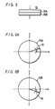
- Fig. 5 is a diagram showing an example of the optical low pass filter according to this invention.
- reference numeral 10 generally designates the optical low pass filter and this optical low pass filter 10 is formed of two double refraction plates, i.e., crystal plates 10A and 10B in this embodiment.
- the first and second crystal plates 10A and 10B have their separating distances d equal to each other.
- the first crystal plate 10A is arranged as shown in Fig. 6A such that its optical axis projection direction 13 relative to the pickup surface of the CCD image sensor 1 has an angle 8 (first quadrant in this embodiment) relative to the horizontal scanning direction H.
- the second crystal plate 10B is arranged as shown in Fig. 6B its optical axis projection direction 14 relative to the pickup surface of the CCD image sensor 1 has an angle-(the fourth quadrant in this embodiment) relative to the horizontal scanning direction H.
- the incident light ray on the first crystal plate 10A is separated to an ordinary light ray (o 1 ) and to an extraordinary light ray (e 1 ) with a distance dtherebetween in the optical axis projection direction 13.
- the light ray incident on the second crystal plate 10B emitted from the first crystal plate 10A is separated to an ordinary light ray ( 02 ) and to an extraordinary light ray (e 2 ) with the distance d therebetween in the optical axis projection direction 14.
- An acute angle 28 between the optical axis projection directions 13 and 14 is selected as where 28 is in the range 0° ⁇ 28 ⁇ 90°.
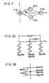
- the incident light ray on the first crystal plate 10A is primarily separated to the ordinary light ray o 1 and the extraordinary light ray e, which are equal in light intensity and are parallel to each other and these two light rays o 1 and e, therefrom become incident on the second crystal plate 10B in which each of them is separated to the ordinary light ray and the extraordinary light ray. Therefore, ax shown in Fig.
- FIG. 7 shows the relation among these light rays o 1 o 2 , o,e 2 , e 1 e 2 and the shape formed by connecting these light rays becomes a lozenge as shown in Fig. 7, and the line formed by connecting the ordinary light ray o l o 2 and the extraordinary light ray e 1 e 2 becomes parallel to the horizontal scanning direction H.
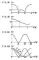
- the frequency of the trap point u 1 is selected to be higherthan 4.5 MHz, it is possible to reduce the occurrence of the moire itself.
- the horizontal residual response at the position of f x1 , and 2f x1 becomes 0.25 so that both carrier components can not be suppressed so effectively.
- the horizontal residual response must be selected to be lower than about 0.1.
- optical axis projection direction does not have to be selected to be at exactly 8 and -8 relative to the horizontal scanning direction H but instead may be near ⁇ and -8.
- the material for forming the double refraction plate is not limited to crystal.
- the field reading method can not be employed as the reading method for the charge transfer in the case of the R and B line sequential signals
- the carrier components in the vertical direction can be reduced by carrying out vertical interpolation processing in the signal processing system provided, after the color separation and sample-and-hold operation, thus causing no trouble in practical use.
- an optical low pass filter 10 which can suppress the carrier component that is harmful to the reproduction the picture image.
- an optical low pass filter 10 can be formed by simply laminating the two crystal plates 10A and 10B, it is possible to reduce the number of crystal plates to be used as compared with the prior art, and it is also possible to laminate the crystal plates accurately and rapidly. Accordingly, it is possible to provide an optical low pass filter which is inexpensive, high in yield and excellent in cost performance.
- the optical low pass filter of this invention is very suitable for being applied to the optical system of an image sensing apparatus using solid state image sensing devices formed of CCD, MOS and the like.
Landscapes
- Physics & Mathematics (AREA)
- General Physics & Mathematics (AREA)
- Optics & Photonics (AREA)
- Color Television Image Signal Generators (AREA)
Claims (6)
Applications Claiming Priority (2)
| Application Number | Priority Date | Filing Date | Title |
|---|---|---|---|
| JP59201355A JPH0772769B2 (ja) | 1984-09-26 | 1984-09-26 | 固体撮像装置 |
| JP201355/84 | 1984-09-26 |
Publications (3)
| Publication Number | Publication Date |
|---|---|
| EP0176334A2 EP0176334A2 (fr) | 1986-04-02 |
| EP0176334A3 EP0176334A3 (en) | 1986-07-30 |
| EP0176334B1 true EP0176334B1 (fr) | 1988-11-17 |
Family
ID=16439663
Family Applications (1)
| Application Number | Title | Priority Date | Filing Date |
|---|---|---|---|
| EP85306749A Expired EP0176334B1 (fr) | 1984-09-26 | 1985-09-23 | Filtre passe-bas optique |
Country Status (5)
| Country | Link |
|---|---|
| US (1) | US4743100A (fr) |
| EP (1) | EP0176334B1 (fr) |
| JP (1) | JPH0772769B2 (fr) |
| CA (1) | CA1271067A (fr) |
| DE (1) | DE3566308D1 (fr) |
Families Citing this family (13)
| Publication number | Priority date | Publication date | Assignee | Title |
|---|---|---|---|---|
| JPH058579Y2 (fr) * | 1985-01-18 | 1993-03-03 | ||
| DE3686358T2 (de) * | 1985-05-27 | 1993-02-25 | Sony Corp | Optischer tiefpassfilter fuer eine festkoerper-farbkamera. |
| US5477381A (en) * | 1989-02-02 | 1995-12-19 | Canon Kabushiki Kaisha | Image sensing apparatus having an optical low-pass filter |
| JP2615248B2 (ja) * | 1989-07-10 | 1997-05-28 | 富士写真フイルム株式会社 | 光学フイルタ |
| US5581301A (en) * | 1990-10-03 | 1996-12-03 | Canon Kabushiki Kaisha | Image processing apparatus with adjustable low-pass optical filter characteristics |
| JP2921163B2 (ja) * | 1991-04-08 | 1999-07-19 | キヤノン株式会社 | 光学的ローパスフィルターを有した撮像装置 |
| US5691830A (en) * | 1991-10-11 | 1997-11-25 | International Business Machines Corporation | Holographic optical system including waveplate and aliasing suppression filter |
| US5337085A (en) * | 1992-04-10 | 1994-08-09 | Comsat Corporation | Coding technique for high definition television signals |
| JPH06169415A (ja) * | 1992-11-30 | 1994-06-14 | Olympus Optical Co Ltd | 撮像装置 |
| JPH09509508A (ja) * | 1994-12-22 | 1997-09-22 | フィリップス エレクトロニクス ネムローゼ フェンノートシャップ | 2個の複屈折性光学フィルタ素子を有する光学的ローパスフィルタ |
| US7116370B1 (en) | 2000-03-31 | 2006-10-03 | Sharp Laboratories Of Ameria, Inc. | Image processing system optical shifting mechanism |
| JP2004126384A (ja) * | 2002-10-04 | 2004-04-22 | Pentax Corp | 光学式ローパスフィルタおよび撮像光学系 |
| JP2004317761A (ja) * | 2003-04-16 | 2004-11-11 | Toyo Commun Equip Co Ltd | 複合型波長板 |
Family Cites Families (6)
| Publication number | Priority date | Publication date | Assignee | Title |
|---|---|---|---|---|
| JPS5850336B2 (ja) * | 1975-04-29 | 1983-11-10 | ソニー株式会社 | 光学的ロ−パスフィルタ |
| JPS5266449A (en) * | 1975-11-28 | 1977-06-01 | Sony Corp | Optical filter |
| JPS5445152A (en) * | 1977-09-17 | 1979-04-10 | Victor Co Of Japan Ltd | Optical comb type filter |
| JPH0620316B2 (ja) * | 1982-05-17 | 1994-03-16 | 株式会社日立製作所 | 撮像光学系 |
| JPS5975222A (ja) * | 1982-10-22 | 1984-04-27 | Victor Co Of Japan Ltd | 光学フイルタ |
| US4575193A (en) * | 1984-04-06 | 1986-03-11 | Eastman Kodak Company | Optical spatial frequency filter |
-
1984
- 1984-09-26 JP JP59201355A patent/JPH0772769B2/ja not_active Expired - Lifetime
-
1985
- 1985-09-05 CA CA000490065A patent/CA1271067A/fr not_active Expired - Lifetime
- 1985-09-16 US US06/776,478 patent/US4743100A/en not_active Expired - Lifetime
- 1985-09-23 EP EP85306749A patent/EP0176334B1/fr not_active Expired
- 1985-09-23 DE DE8585306749T patent/DE3566308D1/de not_active Expired
Also Published As
| Publication number | Publication date |
|---|---|
| DE3566308D1 (en) | 1988-12-22 |
| JPH0772769B2 (ja) | 1995-08-02 |
| CA1271067A (fr) | 1990-07-03 |
| EP0176334A3 (en) | 1986-07-30 |
| US4743100A (en) | 1988-05-10 |
| EP0176334A2 (fr) | 1986-04-02 |
| JPS6177821A (ja) | 1986-04-21 |
Similar Documents
| Publication | Publication Date | Title |
|---|---|---|
| EP0094676B1 (fr) | Système optique pour tube de caméra | |
| US3911479A (en) | Color selective low pass filter | |
| US4743100A (en) | Optical low pass filter | |
| US4101929A (en) | Color encoding video system with optical low pass filter | |
| US4539584A (en) | Television camera having an optical filter | |
| EP0449325B1 (fr) | Filtre optique passe-bas | |
| US4100570A (en) | Optical image pickup system | |
| EP0098559B1 (fr) | Dispositif de prise de vues en couleur à corps solide | |
| US5069530A (en) | Solid state image pick-up apparatus | |
| US3582984A (en) | Color video signal generating apparatus | |
| US3641255A (en) | Noninteracting lens system for a color encoding camera | |
| JPH0415669B2 (fr) | ||
| US3828121A (en) | Color signal producing system utilizing spatial color encoding and comb filtering | |
| US3588326A (en) | Lens array imaging system for a color enconding camera | |
| US3763312A (en) | Optical system for photographic film televising apparatus | |
| JP2840619B2 (ja) | 光学的ローパスフイルタ | |
| KR100272103B1 (ko) | 광저역통과필터 | |
| US3619489A (en) | Shadowing system for color encoding camera | |
| US4417272A (en) | Color television camera having a color separation crossing striped filter | |
| US3757033A (en) | Shadowing system for color encoding camera | |
| USRE28702E (en) | Noninteracting lens system for a color encoding camera | |
| JP2723910B2 (ja) | 固体撮像装置 | |
| JP2508499B2 (ja) | 光学的ロ―パスフィルタ | |
| JPS5838030B2 (ja) | 単管式カラ−テレビジヨンカメラの偽信号除去方式 | |
| US3548089A (en) | Color video signal generating device |
Legal Events
| Date | Code | Title | Description |
|---|---|---|---|
| PUAI | Public reference made under article 153(3) epc to a published international application that has entered the european phase |
Free format text: ORIGINAL CODE: 0009012 |
|
| 17P | Request for examination filed |
Effective date: 19850928 |
|
| AK | Designated contracting states |
Kind code of ref document: A2 Designated state(s): DE FR GB NL |
|
| PUAL | Search report despatched |
Free format text: ORIGINAL CODE: 0009013 |
|
| AK | Designated contracting states |
Kind code of ref document: A3 Designated state(s): DE FR GB NL |
|
| 17Q | First examination report despatched |
Effective date: 19871207 |
|
| GRAA | (expected) grant |
Free format text: ORIGINAL CODE: 0009210 |
|
| AK | Designated contracting states |
Kind code of ref document: B1 Designated state(s): DE FR GB NL |
|
| REF | Corresponds to: |
Ref document number: 3566308 Country of ref document: DE Date of ref document: 19881222 |
|
| ET | Fr: translation filed | ||
| PLBE | No opposition filed within time limit |
Free format text: ORIGINAL CODE: 0009261 |
|
| STAA | Information on the status of an ep patent application or granted ep patent |
Free format text: STATUS: NO OPPOSITION FILED WITHIN TIME LIMIT |
|
| 26N | No opposition filed | ||
| REG | Reference to a national code |
Ref country code: GB Ref legal event code: IF02 |
|
| PGFP | Annual fee paid to national office [announced via postgrant information from national office to epo] |
Ref country code: NL Payment date: 20040905 Year of fee payment: 20 |
|
| PGFP | Annual fee paid to national office [announced via postgrant information from national office to epo] |
Ref country code: FR Payment date: 20040908 Year of fee payment: 20 |
|
| PGFP | Annual fee paid to national office [announced via postgrant information from national office to epo] |
Ref country code: DE Payment date: 20040916 Year of fee payment: 20 |
|
| PGFP | Annual fee paid to national office [announced via postgrant information from national office to epo] |
Ref country code: GB Payment date: 20040922 Year of fee payment: 20 |
|
| PG25 | Lapsed in a contracting state [announced via postgrant information from national office to epo] |
Ref country code: GB Free format text: LAPSE BECAUSE OF EXPIRATION OF PROTECTION Effective date: 20050922 |
|
| PG25 | Lapsed in a contracting state [announced via postgrant information from national office to epo] |
Ref country code: NL Free format text: LAPSE BECAUSE OF EXPIRATION OF PROTECTION Effective date: 20050923 |
|
| REG | Reference to a national code |
Ref country code: GB Ref legal event code: PE20 |
|
| NLV7 | Nl: ceased due to reaching the maximum lifetime of a patent |
Effective date: 20050923 |