EP0176377B1 - Vorrichtung zur autonomen Stromversorgung insbesondere für ein stereoskopisches Beobachtungsgerät - Google Patents
Vorrichtung zur autonomen Stromversorgung insbesondere für ein stereoskopisches Beobachtungsgerät Download PDFInfo
- Publication number
- EP0176377B1 EP0176377B1 EP85401533A EP85401533A EP0176377B1 EP 0176377 B1 EP0176377 B1 EP 0176377B1 EP 85401533 A EP85401533 A EP 85401533A EP 85401533 A EP85401533 A EP 85401533A EP 0176377 B1 EP0176377 B1 EP 0176377B1
- Authority
- EP
- European Patent Office
- Prior art keywords
- switches
- power supply
- voltage
- control
- switching component
- Prior art date
- Legal status (The legal status is an assumption and is not a legal conclusion. Google has not performed a legal analysis and makes no representation as to the accuracy of the status listed.)
- Expired
Links
Images




Classifications
-
- H—ELECTRICITY
- H01—ELECTRIC ELEMENTS
- H01R—ELECTRICALLY-CONDUCTIVE CONNECTIONS; STRUCTURAL ASSOCIATIONS OF A PLURALITY OF MUTUALLY-INSULATED ELECTRICAL CONNECTING ELEMENTS; COUPLING DEVICES; CURRENT COLLECTORS
- H01R13/00—Details of coupling devices of the kinds covered by groups H01R12/70 or H01R24/00 - H01R33/00
- H01R13/02—Contact members
- H01R13/04—Pins or blades for co-operation with sockets
-
- G—PHYSICS
- G02—OPTICS
- G02F—OPTICAL DEVICES OR ARRANGEMENTS FOR THE CONTROL OF LIGHT BY MODIFICATION OF THE OPTICAL PROPERTIES OF THE MEDIA OF THE ELEMENTS INVOLVED THEREIN; NON-LINEAR OPTICS; FREQUENCY-CHANGING OF LIGHT; OPTICAL LOGIC ELEMENTS; OPTICAL ANALOGUE/DIGITAL CONVERTERS
- G02F1/00—Devices or arrangements for the control of the intensity, colour, phase, polarisation or direction of light arriving from an independent light source, e.g. switching, gating or modulating; Non-linear optics
- G02F1/01—Devices or arrangements for the control of the intensity, colour, phase, polarisation or direction of light arriving from an independent light source, e.g. switching, gating or modulating; Non-linear optics for the control of the intensity, phase, polarisation or colour
- G02F1/03—Devices or arrangements for the control of the intensity, colour, phase, polarisation or direction of light arriving from an independent light source, e.g. switching, gating or modulating; Non-linear optics for the control of the intensity, phase, polarisation or colour based on ceramics or electro-optical crystals, e.g. exhibiting Pockels effect or Kerr effect
- G02F1/055—Devices or arrangements for the control of the intensity, colour, phase, polarisation or direction of light arriving from an independent light source, e.g. switching, gating or modulating; Non-linear optics for the control of the intensity, phase, polarisation or colour based on ceramics or electro-optical crystals, e.g. exhibiting Pockels effect or Kerr effect the active material being a ceramic
- G02F1/0555—Operation of the cell; Circuit arrangements
-
- G—PHYSICS
- G03—PHOTOGRAPHY; CINEMATOGRAPHY; ANALOGOUS TECHNIQUES USING WAVES OTHER THAN OPTICAL WAVES; ELECTROGRAPHY; HOLOGRAPHY
- G03B—APPARATUS OR ARRANGEMENTS FOR TAKING PHOTOGRAPHS OR FOR PROJECTING OR VIEWING THEM; APPARATUS OR ARRANGEMENTS EMPLOYING ANALOGOUS TECHNIQUES USING WAVES OTHER THAN OPTICAL WAVES; ACCESSORIES THEREFOR
- G03B35/00—Stereoscopic photography
- G03B35/16—Stereoscopic photography by sequential viewing
Definitions
- the present invention relates to an autonomous power supply device for observation device provided with at least one electro-optical cell with capacitive effect containing an electro-optical material cooperating with a system of control electrodes receiving electrical signals d 'high amplitude, and comprising clock means to allow the control of the periodic application of electrical control signals on the electrode system of electrooptical cells.
- the right device and the left device each comprise an electro-optical cell with a capacitive effect constituted by an electro-optical material, for example of the PLZT type and associated control electrodes.
- Control voltages are applied alternately to the control electrodes of the two cells to alternately allow the transmission of light through the right and left devices which each include such a cell, and thereby create a stereoscopic effect.
- the alternative application of the control voltages to the right and left devices of the pair of glasses must also be related to the laws of image sequencing.
- the apparatus for observing images with a stereoscopic effect must then be equipped with means for receiving said modulated carrier wave in order to allow the extraction of synchronization information from the alternative application of control voltages to the right and left of the pair of glasses.
- control voltages applied to electro-optic cells with a capacitive effect are particularly high, and can be of the order of 1000 V. Consequently, the use of such voltage levels can prove dangerous for the user of the image observation equipment with stereoscopic effect, particularly if the high voltage generator is directly mounted on the pair of glasses.
- the high voltage required is first generated in a high voltage generator circuit capable of permanently delivering a high voltage, and this high voltage is then switched alternately on each pair of electrodes associated with a cell.
- the switches operating on a permanent continuous high voltage are relatively complex.
- the object of the present invention is precisely to remedy the aforementioned drawbacks and to produce an autonomous power supply device which has great security, a small footprint, reduced energy consumption and good stability of the signals generated, while offering a possibility voltage adjustment, to take account of dispersions, and a high speed of switching on highly capacitive loads.
- a supply device of the type defined at the head of the description which, in accordance with the invention comprises a low voltage power source, a circuit for intermittently creating a high voltage from the low voltage power source, a set of switches interposed between the intermittent high voltage creation circuit and the electrode system of said electrooptical cells, and clock signal processing circuits for synchronized control said intermittent high voltage creation circuit and said co-switches.
- the invention thanks to the presence of a high voltage generator of the pulsed type, ensures the storage of energy at low voltage, and does not work at high voltage until the transfer of energy to the electrooptical cells. It is thus possible to control the value of the intensity of the currents involved, and especially to provide energy to the electrooptic cells only at the previous transitions of the commutations of the state of these cells, since, by their Capacitive in nature, the electrooptical cells can remain polarized even when disconnected from the high voltage source.
- the invention also easily provides energy recovery when switching from one cell to another.
- the present invention is applicable both to viewing devices of the window type comprising a single capacitive effect electrooptical cell and to devices observation type glasses comprising first and second electrooptical cells with capacitive effect each cooperating with an electrode system.
- the clock signal processing circuits may include synchronization means capable of receiving an external synchronization signal for sequentially controlling said intermittent high voltage creation circuit and said switches.
- the autonomous power supply device applied to observation glasses with stereoscopic effect, comprises means for receiving a carrier wave modulated by synchronization signals to allow the control of the synchronized periodic application of electrical signals of high amplitude control alternately on the electrode systems of said first and second cells, the clock signal processing circuits include means for processing the synchronization signals received by said means reception for sequentially controlling said intermittent high voltage creation circuit and said switches.
- the intermittent high voltage creation circuit comprises an inductor and a switching member connected in series across the terminals of the low voltage power source, as well as a capacitor mounted in parallel on the switching member, and said switching member is periodically controlled from the signal processing circuits.
- the device according to the invention comprises a first switch mounted between the common point of the inductance and of the switching member and an electrode of one of the electrooptical cells with capacitive effect, and said first switch is controlled by so as to be closed from the start of the opening of the switching member and for a time less than the opening time of said switching member.
- the autonomous power supply device may further comprise a second switch mounted between said electrode of one of the electrooptical cells and the end of the connected inductor, by means of a non-return source diode. low voltage power supply and said second switch is controlled so as to be closed from the start of the closing of the switching member and for a time less than the closing time of said switching member.
- the autonomous power supply device comprises first and third switches mounted between on the one hand the common point of the inductor and the switching member and, on the other hand, an electrode of the first and second electro-optical cells respectively, and second and fourth switches mounted between on the one hand the end of the connected inductor, via a non-return diode to the low voltage power source and on the other share respectively the common point between the first switch and the first electro-optical cell and the common point between the third switch and the second electro-optical cell, the first and fourth earphones are controlled so as to be closed simultaneously from the start of the opening of the switching device, every two periods of the switching device control signal while the second and third switches are controlled so as to be closed simultaneously from the start of the opening of the switching device during the periods of the switching device control signal where the first and fourth switches remain permanently open, and the closing time of the first and second, third and fourth switches is each time less than the duration of opening of the switching member.
- a clipping diode is mounted in parallel on the capacitor arranged in parallel on the switching member and a protection diode can also be connected in series with said switching member across said capacitor.
- the device according to the invention comprises a circuit for modulating the duration of control of the closing of the cummutation member.
- the device may include a divider bridge for measuring the high voltage applied periodically to the common point of the inductor and the switching member, a blocking sampler circuit, a comparator between the sampled voltage and a reference voltage. V ref and a circuit for applying a delay, as a function of the value of the output signal of said comparator, to the signal for controlling the transition to the closed state of the switching member.
- the circuits for processing the synchronization signals received by the reception means can comprise a phase control circuit, as well as a matrix of programmable logic circuits for controlling the switching sequences of the switches.
- the switches are floating control and include a high voltage switching device, such as a bipolar transistor, a field effect transistor or a thyristor, mounted diagonally of a diode bridge, and a coupler for applying a control signal to the switching device.
- a high voltage switching device such as a bipolar transistor, a field effect transistor or a thyristor, mounted diagonally of a diode bridge, and a coupler for applying a control signal to the switching device.
- the coupler is preferably of the piezoelectric coupler or linear transformer type at resonance.
- the low-voltage power source, the intermittent high-voltage creation circuit, the set of switches and the synchronization signal processing circuits are combined in a portable box connected to the reception means and to the first and second cells. by three or four connecting wires.
- all of the switches are floating control and provide bipolar control of the high voltage applied to the electrodes of the first and second electrooptical cells.
- the set of switches provides unipolar control of the high voltage applied to the electrodes of the first and second electro-optical cells.
- the switches may each comprise a field effect transistor, an auxiliary capacitor mounted between the gate and the source of said field effect transistor, a diode connected in series with the drain-source space of said effect transistor. field, and a coupler.
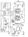
- FIG. 1 shows the general diagram of a self-contained feeding device for a pair of stereoscopic effect image observation glasses 50 comprising a subassembly 30 with a right device 31 and a left observation device 32 intended to come next to the right and left eyes of the observer respectively.
- the spectacle frame making it possible to place the right and left devices 31, 32 in front of the eyes of the observer can be of conventional structure, with two branches intended to bear on the ears of the observer and an anterior frontal part intended to support the right and left devices 31, 32.
- the right and left devices 31, 32 each comprise an electrooptical material disposed between two electrodes.
- the material can be of the PLZT type for example.
- the electrodes can for example be constituted by a network of interdigitated electrodes deposited on each of the faces of the crystal.
- the devices 31, 32 are thus constituted by electrooptical cells with a capacitive effect which, if they are placed between crossed polarizers, can alternatively allow or prevent the transmission of light depending on whether or not a control voltage is applied to the electrodes of the cell.
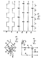
- FIG. 10 shows for cell 31 of a right device (curve 201) and for cell 32 d 'a left device (curve 202) the state change sequences between the opening state 0 (light transmission) and the closing state F (non-light transmission).
- FIG. 11 shows an example of an electrical sequence for controlling cells 31, 32, of the bipolar type, with the form of the high voltage electrical signals which can be applied to the pairs of electrodes of cells 31, 32 (curves 203, 204 respectively) to create the state change sequences in Figure 10.
- FIG. 12 shows another example of an electrical sequence for controlling cells 31, 32, of the unipolar type, with the shape of the high voltage electrical signals which can be applied to the pairs of electrodes of cells 31, 32 (curves 205, 206 respectively) to create the state change sequences of FIG. 10.
- the electrical control signals of the cells 31, 32 are represented by periodic signals of square shape applied in alternating sequence to the pairs of electrodes of the cells 31, 32. This essentially corresponds to the signals present at the terminals of each of the cells when they are in service.
- the real time of connection of a pair of electrodes to a high-voltage generator is less than the duration of the application of this voltage to the cell.
- an electro-optical cell 31, 32 can keep its charge while remaining polarized, even after the connection to the high-voltage generator has been removed.
- the invention thus essentially implements a power supply device comprising a sequential high voltage generator 20 which supplies high voltage energy in a pulsed manner and provides internal energy storage only in the form of low voltage. Thanks to the set 90 of switches, which direct and control the impulse application of a high voltage to the cells 31, 32, energy is only supplied to the cells 31, 32 at the previous transitions of the switching operations.
- pilot For the observation of television images, it is necessary to have a pilot signal synchronized with the scanning of the television receiver, and to synchronize the alternative application of the control signals to the cells 31, 32 on the basis of this signal.
- the pilot signal can be obtained from a carrier wave for example of the infrared type modulated from scanning synchronization signals and picked up by an infrared cell 41 disposed in the pair of glasses within a device. 40 for carrier wave reception.
- a single cable e can be used both to supply the reception device 40 with a low supply voltage and to convey a high frequency AC component superimposed on the DC voltage signal and representing the signal pilot picked up by the infrared cell 41.
- FIG. 1 a single cable e can be used both to supply the reception device 40 with a low supply voltage and to convey a high frequency AC component superimposed on the DC voltage signal and representing the signal pilot picked up by the infrared cell 41.
- a carrier amplifier 42 which receives the signals delivered by the sensor 41, a link capacitor 43 , disposed between the output of amplifier 42 and the connection cable e, as well as an inductance 44 and a capacitor 45 constituting a separator between the high frequency and the low supply voltage, disposed between the connection cable a and a regulator 46 for supplying the circuits of the reception device 40.
- the receiving device 40, as well as the device 30 with electro-optical cells 31, 32 are arranged in the spectacle frame proper, while the autonone supply device of the devices 30 and 40 is contained in an independent, portable housing.
- low volume connected to devices 30 and 40 by connecting wires a, b, c, d and e.
- the wires a and b are connected to the electrodes of the right cell 31 while the wires c and d are connected to the electrodes of the left cell 32.
- the wires b and d are connected to ground and can thus be formed by a single ground wire.
- the actual autonomous power supply device for applying high voltage control signals to the electrodes of the electrooptical cells 31, 32 comprises a low voltage power supply source BT, a circuit 20 for intermittently creating a positive high voltage or negative from the power source BT, a set of floating control switches 1 to 16, and circuits 100 for processing the synchronization signals received by the reception device 40 and transmitted on the line e.
- the processing circuits 100 include a circuit 110 for shaping the synchronization signals applied from the line e via a connecting capacitor 101.
- the inductor 102 and the capacitor 103 are used for the separation of the supply side, between the low voltage power supply signals from the LV source and the HF synchronization signals received by the line e.
- the processing circuits 100 further comprise logic sequencing circuits 190 which may include a programmable logic network (PLA) and ensure the synchronized sequential production of control signals from the switches 1 to 16 and from the circuit 20 for creating a high voltage. .
- logic sequencing circuits 190 may include a programmable logic network (PLA) and ensure the synchronized sequential production of control signals from the switches 1 to 16 and from the circuit 20 for creating a high voltage.
- PLA programmable logic network
- the floating control switches 1 to 16 can thus comprise a high voltage switching member 65, such as a bipolar transistor, a field effect transistor or a thyristor, mounted in the diagonal of a diode bridge 61 to 64, and a coupler 67 connected to the logic processing circuits 190 for the application of a control signal to the switching member 65.
- a simple or composite element 66, capacitive, resistive or inductive, and optionally non-linear can also be mounted in series with the switching unit 65 to allow modification of the switching operations.
- the switching circuit 90 of FIG. 1 represents the general case making it possible, by adapting the characteristics of the various switches 1 to 16, to control in a very diverse way a pair of electrooptical cells 31, 32 from a pulsed or alternating high voltage source produced intermittently and periodic in a circuit 20 supplied with low voltage.
- the circuit 90 of FIG. 1, adapted to a bipolar control, allows in particular charge transfers from one electrooptical cell 31 to the other 32 and vice versa, and various regimes of energy recovery in low voltage sources, same as standby modes for which the electro-optical cell 31 or 32 retains its charge in floating mode. It also allows rapid short circuits of cells 31, 32, allowing dynamic resets.
- the switches of these cells can be replaced by equivalent components or even in certain cases by short-circuits.
- maximum flexibility is provided due to the configuration implementing for each cell two successive series of switches mounted in a bridge.
- the control of the right-hand cell 31 may involve a first series of switches connected in bridge 9, 1, 5 and 13, then a second series of switches also connected in bridge 10, 2, 6, 14.
- the configuration of the switches controlling the left cell 32 is itself symmetrical to that of the switches controlling the right cell.
- the switches 1, 9, 5, 13 respectively 3, 11, 7, 15 of the first bridge associated with the right cell 31 respectively with the left cell 32 control the application of the high voltage on the controlled cell 31 respectively 32 while the switches 2,10,6,14 resp. 4, 16, 8, 12 of the second bridge associated with the right cell 31 resp. to the left cell 32 control the energy transfers from a cell 31 resp. 32 to the other 32 resp. 31.
- Figure 2 shows a particular embodiment of the device of Figure 1 and shows the structure of the high voltage pulsed source 20. Similar elements in the different circuits of the different figures have the same references and can thus be more easily identified.
- the devices 30, 40 of the pair of glasses 50, and the circuits 100 having already been described with reference to FIG. 1, these will not be described again.
- the only difference consists in joining the connection wires b and d into a single ground wire.
- FIG. 2 shows a high voltage power source 20 supplied from a low voltage source LV and comprising a switching member 21 constituted by a transistor controlled by the logic processing circuits 190.
- the presence of this switching member 21 associated with that of a constant current charging element (inductance 22) makes it possible to create from a quantized energy a high voltage in an impulse fashion and to store in the generator 20 no energy in the form of high tension.
- the floating control switches 1, 3, the constitution of which can be similar to that shown in FIG. 3, ensure the switching of the high voltage to the electrodes of the right cell 31 and of the left cell 32 respectively.
- Switches 2 and 4 with floating control have a structure similar to that of switches 1 and 3 and play a role which will be explained below with reference to the time diagram in FIG. 5.
- Switches 1, 2, 3, 4 are controlled by circuits 91, 92, 93, 94 respectively which receive signals from the logic circuits 190 for controlling the switching sequences.
- the circuits 91, 92, 93, 94 may have a structure similar to that shown in FIG. 4 with a transistor 71 whose base receives the control signal from the logic circuits 190, and a capacitor 73 mounted in parallel on the space collector-emitter of transistor 71.
- the control signal applied to the coupler 67 of the switch to be controlled is taken from the collector of transistor 71.
- a limiting resistor 72 and a diode 74 can be mounted in series between the coupler 67 and the collector of the transistor 71.
- the base of the transistor 71 is furthermore connected to ground by a resistor 75.
- the inductor 22 is connected on the one hand to the low voltage power source BT by means of a non-return diode 25 and, on the other hand, to a common point 28 for producing a high voltage .
- a capacitor 23 whose value remains low compared to that of the capacitive cells 31, 32 and may for example be of the order of a tenth of it is connected between the common point 28 and the ground.
- the collector of transistor 21 is itself connected to the common point 28 via a protection diode 24 which prohibits the application of any reverse voltage on the transistor 21.
- a clipping diode for negative voltages 27, in series with a switch 26 is further connected between said common point 28 and ground.
- the switches 2 and 4 are themselves connected between the connection wires a, respectively for applying the high voltage to the cells 31, 32 respectively and on the other hand at the connection point of the inductor 22 with the LV low voltage power supply.
- Switch 26 is controlled by a circuit 97 analogous to circuits 91 to 94 and receiving signals from logic control circuits 190.
- the operation of the circuit 20 for producing a high voltage is as follows: in a first period of time the transistor 21 is made conductive and allows the passage of a current in the inductor 22 from the low voltage source of food.
- the current in the transistor 21 and therefore at the common point 28 increases practically linearly as a function of time from the initial instant of closing of the transistor 21.
- the circuit is abruptly opened at the common point 28 and the current stored in the inductor 22 is discharged in the capacitor 23 and, depending on whether the switch 1 or 3 is energized and closed, in the capacitive cell 31 or the capacitive cell 32
- the voltage at point 28 then presents a marked positive excursion, allowing the application of a high voltage on one of the cells 31, 32.
- the capacitor 23 essentially serves to avoid excessively steep sides during the rise of the voltage excursion at point 28 and avoid excessively rapid overshoots.
- the switch 1, respectively the switch 3 are controlled so as to remain closed for a time less than the opening of the switching member constituted by the transistor 21.
- control sequences are possible and allow the recovery of a greater or lesser energy during the passage of control of a cell 31 resp. 32 to the other 32 resp. 31.
- the command sequences can also take account of disparities between cells 31 and 32 and present two different actions every second time.
- the circuit of FIG. 6, which allows control of the voltage at the output point 28 in the manner shown in FIG. 7, also contributes to giving greater flexibility of use to the autonomous supply device according to the invention.
- the modulation of the conduction control duration of transistor 21 makes it possible to adjust the maximum voltage available at point 28 to be applied to cells 31, 32.
- FIG. 7 shows on the one hand the aspect of the evolution of the current IL flowing in the inductor 22 during the different successive periods during the conduction time of the transistor 21 and on the other hand the shape of the voltage Vq l available at the output point 28 during the opening of the transistor 21 during the different successive periods.
- the delay 8 For the determination of the delay 8 to be applied at the start of the control of the conduction of the transistor 21, it is necessary to detect the value of the maximum voltage present at the opening of the transistor 21 on the output 28, then to compare the detected value with the desired value and finally to apply the difference to a device for modifying the conduction time of transistor 21 by inserting a delay ⁇ with respect to the scheduled order date.
- This is achieved by a circuit of the type of that of FIG. 6 by which the voltage at the output point 28 is taken using a divider bridge 81, 82 to be applied to a sampler-block circuit 83.
- the output of the sample-and-hold circuit 83 is applied to a first input of a comparator circuit 84 receiving at its other input a reference voltage U o .
- the comparator error signal 84 is then applied to a processing circuit 131 also receiving synchronization pulses linked to the signal delivered by the receiving device 40.
- a processing circuit 131 comprising a phase servo component (PLL circuit) which makes it possible to generate phase-shifted signals, from an incident synchronization frequency.
- the phase difference with respect to the control is determined by the error voltage of the comparator 84 and thus makes it possible to produce a voltage control.
- the couplers 67 used in combination with the floating control switches such as that shown in FIG. 3 can be constituted in a conventional manner by optocouplers or transformers. However, it is preferable to use piezoelectric ceramic resonators used as couplers, or linear transformers used for resonance, in particular for reasons of energy saving and ease of obtaining high voltage known as "mode". common "of the switch component.
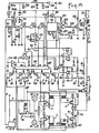
- FIG. 8 represents the detailed diagram of an exemplary embodiment of an autonomous power supply device in accordance with the invention and making it possible to perform bipolar control of the electrooptical cells 31, 32.
- the diagram of FIG. 8 thus follows from the general diagram of figure 1.
- a LV low voltage power source comprising a storage battery 106 which can be recharged through a diode 105 from an external source 104, a reservoir capacitor 107, a general switch 108, and indicators 109, 109a of the state of the low voltage source.
- the HF signals from the device 40 for receiving a modulated carrier wave are, after separation of the low voltage supply signals, applied to a preamplifier 111, 112, 113, then to a shaping stage 110 comprising a circuit smoothing 114,115,116, 117 or decoding.
- the signals from the shaping stage 110 are then subjected to successive phase shifts by the circuits 121, 122, 123 and applied to a component 131 with phase lock loop to which the error signal of a comparator is also applied. 84.
- the output signals of the circuit 131 with phase-locked loop, supplied by a supply voltage regulated by the transistor 118, are applied via a link capacitor 207 and a control circuit 202 to 206 at the base of transistor 21 serving as a high voltage cutter, the collector of which is connected by diode 24 to the tank inductor 22.
- the processing logic circuits 100 comprise a programmed or programmable logic unit 191 which generates the switching sequences by delivering control signals which, via control circuits 91 to 96 are applied to the primers of the couplers 67 of the switches 1, 2, 3, 4, 17, 18 with floating control.
- the logic processing circuits 100 further comprise a parity indicator 124 with light-emitting diode 125, connected at the output of the phase shifters 122 and 123. Furthermore, it is associated with the divider bridge 81, 81 a, 82, with the sample-and-hold circuit 83 and to the composer 84 which control the phase shift applied by the circuit 131, locking and inhibition circuits 143, 144, a monostable 142 and an oscillator 141.
- FIG. 9 represents a simplified version of the device of FIG. 8.
- the device of FIG. 9 provides unipolar type control of the electrooptical cells 31 and 32 and comprises only four switches 1 to 4 which, due to the unipolar control can not understand that a single bipolar transistor or field effect transistor 65, a capacitor 68 associated with the coupler 67 and a diode 61 to replace the diode bridge of the switches of the device of FIG. 8.
- the couplers 67 two double linear transformers in place of the four simple transformers of the embodiment of FIG. 8, taking into account the synchronicity of control of the transistors 65 of the switches 1 to 4 two by two.
- the logic control circuits 100 can be simplified due to the simplicity of the sequence.
- the autonomous supply device is suitable for supplying spectacles which, depending on the type of control adopted, may or may not allow stereoscopic vision.
- FIG. 13 shows the shape of the optical transmission sequences 301, 302 applied to the right electrooptical cells 31 and left 32 respectively of glasses in the case where an internal synchronizable clock punctuates the periodic creation of a high voltage by the circuit of power supply 20 without the intervention of an external synchronization signal.
- FIG. 13 relates by way of example to an identical synchronous control for the two cells 31 and 32 in which the cells 31, 32 are most of the time in the open state O and comprise only brief periodic interruptions of optical transmission.
- FIG. 14 shows optical transmission sequences 303 and 304 applied to the right and left electrooptical cells 31 in a case very similar to that of FIG. 13 but where, depending on the control of the power supply device, the brief periodic interruptions of optical transmission of one cell 31 are offset in time with respect to the periodic interruptions of optical transmission of the other cell 32.
- FIG. 15 shows optical transmission sequences 305 and 306 applied to the right electrooptical cells 31 and left 32 in the case where it is desired to obtain a stereoscopic effect
Landscapes
- Physics & Mathematics (AREA)
- Chemical & Material Sciences (AREA)
- Engineering & Computer Science (AREA)
- Ceramic Engineering (AREA)
- Nonlinear Science (AREA)
- General Physics & Mathematics (AREA)
- Crystallography & Structural Chemistry (AREA)
- Optics & Photonics (AREA)
- Testing, Inspecting, Measuring Of Stereoscopic Televisions And Televisions (AREA)
- Dc-Dc Converters (AREA)
- Control Of Indicators Other Than Cathode Ray Tubes (AREA)
- Apparatus Associated With Microorganisms And Enzymes (AREA)
Claims (20)
Applications Claiming Priority (2)
| Application Number | Priority Date | Filing Date | Title |
|---|---|---|---|
| FR8412832 | 1984-08-16 | ||
| FR8412832A FR2569281B1 (fr) | 1984-08-16 | 1984-08-16 | Dispositif d'alimentation autonome pour dispositif d'observation, notamment a effet stereoscopique |
Publications (2)
| Publication Number | Publication Date |
|---|---|
| EP0176377A1 EP0176377A1 (de) | 1986-04-02 |
| EP0176377B1 true EP0176377B1 (de) | 1988-12-14 |
Family
ID=9307055
Family Applications (1)
| Application Number | Title | Priority Date | Filing Date |
|---|---|---|---|
| EP85401533A Expired EP0176377B1 (de) | 1984-08-16 | 1985-07-25 | Vorrichtung zur autonomen Stromversorgung insbesondere für ein stereoskopisches Beobachtungsgerät |
Country Status (5)
| Country | Link |
|---|---|
| US (1) | US4732457A (de) |
| EP (1) | EP0176377B1 (de) |
| JP (1) | JPS61191192A (de) |
| DE (1) | DE3566841D1 (de) |
| FR (1) | FR2569281B1 (de) |
Families Citing this family (6)
| Publication number | Priority date | Publication date | Assignee | Title |
|---|---|---|---|---|
| CA2003496C (en) * | 1989-11-21 | 1994-06-07 | Anton Leo Baljet | Projection synchronization system |
| US5002387A (en) * | 1990-03-23 | 1991-03-26 | Imax Systems Corporation | Projection synchronization system |
| US6302876B1 (en) | 1997-05-27 | 2001-10-16 | Visx Corporation | Systems and methods for imaging corneal profiles |
| US6127812A (en) * | 1999-02-16 | 2000-10-03 | General Electric Company | Integrated environmental energy extractor |
| FR2836772B1 (fr) * | 2002-03-04 | 2004-07-09 | Absys | Generateur de gaz pour un systeme de sterilisation |
| CN103347192B (zh) * | 2013-06-29 | 2015-07-08 | 青岛歌尔声学科技有限公司 | 立体眼镜液晶镜片的控制方法和控制装置以及立体眼镜 |
Family Cites Families (8)
| Publication number | Priority date | Publication date | Assignee | Title |
|---|---|---|---|---|
| US3292091A (en) * | 1965-02-24 | 1966-12-13 | Ibm | Energy conserving circuit for capacitive load |
| CA959317A (en) * | 1973-01-31 | 1974-12-17 | Shunsei Kratomi | Stereoscopic apparatus having liquid crystal filter viewer |
| US3879687A (en) * | 1973-02-26 | 1975-04-22 | Honeywell Inc | High speed light beam modulator |
| JPS5528060Y2 (de) * | 1973-09-07 | 1980-07-04 | ||
| FR2264431B1 (de) * | 1974-03-14 | 1976-12-17 | Comp Generale Electricite | |
| DE2632483A1 (de) * | 1975-07-23 | 1977-02-10 | Thorn Electrical Ind Ltd | Stereoskopisches betrachtungssystem und -geraet |
| JPS56111828A (en) * | 1980-02-08 | 1981-09-03 | Matsushita Electric Ind Co Ltd | Stereo spectacles device |
| DE3214021A1 (de) * | 1982-04-16 | 1983-10-20 | Bruker Analytische Meßtechnik GmbH, 7512 Rheinstetten | Vorrichtung zur erzeugung und darstellung dreidimensionaler bilder |
-
1984
- 1984-08-16 FR FR8412832A patent/FR2569281B1/fr not_active Expired
-
1985
- 1985-07-25 DE DE8585401533T patent/DE3566841D1/de not_active Expired
- 1985-07-25 EP EP85401533A patent/EP0176377B1/de not_active Expired
- 1985-07-31 US US06/760,812 patent/US4732457A/en not_active Expired - Fee Related
- 1985-08-15 JP JP60180000A patent/JPS61191192A/ja active Pending
Also Published As
| Publication number | Publication date |
|---|---|
| US4732457A (en) | 1988-03-22 |
| DE3566841D1 (en) | 1989-01-19 |
| EP0176377A1 (de) | 1986-04-02 |
| FR2569281B1 (fr) | 1986-12-05 |
| FR2569281A1 (fr) | 1986-02-21 |
| JPS61191192A (ja) | 1986-08-25 |
Similar Documents
| Publication | Publication Date | Title |
|---|---|---|
| EP0722211B1 (de) | Bidirektionaler Gleichstrom-Gleichstrom-Spannungswandler und Stromsensor | |
| EP2735038B1 (de) | Batterie mit einer backsteinarchitektur mit seriell oder parallel angeordneten zellen | |
| EP0722212B1 (de) | Bidirektionale Gleichstrom-Gleichstrom-Spannungswandler und Stromsensor | |
| EP0326489A1 (de) | Regulierungssystem des Arbeitspunktes einer Gleichstromversorgung | |
| FR2731157A1 (fr) | Stimulateur magnetique pour tissu neuromusculaire | |
| EP0803067A1 (de) | Bidirektionaler gleichspannung-gleichspannung-umformer und stromwandler | |
| EP2102994A2 (de) | Elektrisch isolierte einrichtung zum koppeln von messsignalen und eine solche einrichtung umfassendes elektrisches gerät | |
| WO2011003975A1 (fr) | Nouvelle architecture de compensateur des facteurs de puissance et d'harmoniques pour reseau de distribution d'energie | |
| EP0329571B1 (de) | Schaltungsanordnung zur Überwachung der Entmagnetisierung für einen Sperrwandler mit primärseitiger und secundärseitiger Regelung | |
| CA2047736A1 (fr) | Transmission inductive bidirectionnelle de donnees a station esclave alimentee par le maitre | |
| EP0176377A1 (de) | Vorrichtung zur autonomen Stromversorgung insbesondere für ein stereoskopisches Beobachtungsgerät | |
| CH617298A5 (de) | ||
| CH506910A (fr) | Circuit convertisseur | |
| EP0267252B1 (de) | Frequenzumwandler zur stabilen speisung von asynchronmotoren | |
| FR2667723A1 (fr) | Dispositif d'obtention et de commutation de hautes tensions de polarisation d'electrodes de tube a rayons x. | |
| EP0087541B1 (de) | Stromversorgungsschaltung und eine Übertragungsvorrichtung mit dieser Schaltung | |
| EP1139361A1 (de) | Elektrische Schaltungsanordnung zur Meldung von Zustandsinformationen, insbesondere für Eisenbahnmaterial, und System mit einer solchen Einrichtung | |
| FR2493640A1 (fr) | Circuit electrostatique d'attaque a haute tension utilisant des diodes | |
| EP1410488B1 (de) | Energieumwandlungseinrichtung | |
| EP1493522A1 (de) | Drahtfunkenerosionsmaschine | |
| WO2013144350A1 (fr) | Générateur de courant et procédé de génération d'impulsions de courant | |
| CA2474137C (fr) | Convertisseur statique d'energie electrique destine a moduler l'energie electrique echangee entre au moins une source de tension et une source de courant | |
| EP3185389B1 (de) | Vorrichtung und elektrisches gerät zur erzeugung einer elektrischen spannung für eine informationsbearbeitungseinheit, und entsprechendes elektronisches system zur informationsbearbeitung | |
| FR2698499A1 (fr) | Circuit pour faire fonctionner une charge inductive. | |
| CA1108693A (fr) | Onduleur autonome a modulation de largeur d'impulsions |
Legal Events
| Date | Code | Title | Description |
|---|---|---|---|
| PUAI | Public reference made under article 153(3) epc to a published international application that has entered the european phase |
Free format text: ORIGINAL CODE: 0009012 |
|
| 17P | Request for examination filed |
Effective date: 19850726 |
|
| AK | Designated contracting states |
Kind code of ref document: A1 Designated state(s): BE DE GB IT NL SE |
|
| 17Q | First examination report despatched |
Effective date: 19871218 |
|
| GRAA | (expected) grant |
Free format text: ORIGINAL CODE: 0009210 |
|
| AK | Designated contracting states |
Kind code of ref document: B1 Designated state(s): BE DE GB IT NL SE |
|
| ITF | It: translation for a ep patent filed | ||
| GBT | Gb: translation of ep patent filed (gb section 77(6)(a)/1977) | ||
| REF | Corresponds to: |
Ref document number: 3566841 Country of ref document: DE Date of ref document: 19890119 |
|
| PLBE | No opposition filed within time limit |
Free format text: ORIGINAL CODE: 0009261 |
|
| STAA | Information on the status of an ep patent application or granted ep patent |
Free format text: STATUS: NO OPPOSITION FILED WITHIN TIME LIMIT |
|
| 26N | No opposition filed | ||
| ITTA | It: last paid annual fee | ||
| PGFP | Annual fee paid to national office [announced via postgrant information from national office to epo] |
Ref country code: SE Payment date: 19940629 Year of fee payment: 10 |
|
| PGFP | Annual fee paid to national office [announced via postgrant information from national office to epo] |
Ref country code: GB Payment date: 19940712 Year of fee payment: 10 |
|
| PGFP | Annual fee paid to national office [announced via postgrant information from national office to epo] |
Ref country code: NL Payment date: 19940731 Year of fee payment: 10 |
|
| PGFP | Annual fee paid to national office [announced via postgrant information from national office to epo] |
Ref country code: BE Payment date: 19940810 Year of fee payment: 10 |
|
| PGFP | Annual fee paid to national office [announced via postgrant information from national office to epo] |
Ref country code: DE Payment date: 19940920 Year of fee payment: 10 |
|
| EAL | Se: european patent in force in sweden |
Ref document number: 85401533.6 |
|
| PG25 | Lapsed in a contracting state [announced via postgrant information from national office to epo] |
Ref country code: GB Effective date: 19950725 |
|
| PG25 | Lapsed in a contracting state [announced via postgrant information from national office to epo] |
Ref country code: SE Effective date: 19950726 |
|
| PG25 | Lapsed in a contracting state [announced via postgrant information from national office to epo] |
Ref country code: BE Effective date: 19950731 |
|
| BERE | Be: lapsed |
Owner name: ETAT-FRANCAIS REPRESENTE PAR LE DELEGUE GENERAL PO Effective date: 19950731 |
|
| PG25 | Lapsed in a contracting state [announced via postgrant information from national office to epo] |
Ref country code: NL Effective date: 19960201 |
|
| GBPC | Gb: european patent ceased through non-payment of renewal fee |
Effective date: 19950725 |
|
| NLV4 | Nl: lapsed or anulled due to non-payment of the annual fee |
Effective date: 19960201 |
|
| PG25 | Lapsed in a contracting state [announced via postgrant information from national office to epo] |
Ref country code: DE Effective date: 19960402 |
|
| EUG | Se: european patent has lapsed |
Ref document number: 85401533.6 |