EP0177883B1 - Anordnung zur Trägerrückgewinnung aus empfangenen 2 PSK-Signalen - Google Patents
Anordnung zur Trägerrückgewinnung aus empfangenen 2 PSK-Signalen Download PDFInfo
- Publication number
- EP0177883B1 EP0177883B1 EP85112423A EP85112423A EP0177883B1 EP 0177883 B1 EP0177883 B1 EP 0177883B1 EP 85112423 A EP85112423 A EP 85112423A EP 85112423 A EP85112423 A EP 85112423A EP 0177883 B1 EP0177883 B1 EP 0177883B1
- Authority
- EP
- European Patent Office
- Prior art keywords
- input
- transistors
- transistor
- frequency divider
- emitter
- Prior art date
- Legal status (The legal status is an assumption and is not a legal conclusion. Google has not performed a legal analysis and makes no representation as to the accuracy of the status listed.)
- Expired - Lifetime
Links
- 238000011084 recovery Methods 0.000 title claims abstract description 20
- 230000005669 field effect Effects 0.000 claims abstract description 8
- 239000003990 capacitor Substances 0.000 claims description 18
- 238000004804 winding Methods 0.000 claims description 11
- 230000000295 complement effect Effects 0.000 claims description 3
- 238000011144 upstream manufacturing Methods 0.000 claims 1
- 230000001360 synchronised effect Effects 0.000 description 8
- 230000010363 phase shift Effects 0.000 description 2
- 230000032683 aging Effects 0.000 description 1
- 230000005540 biological transmission Effects 0.000 description 1
- 238000006243 chemical reaction Methods 0.000 description 1
- 230000008878 coupling Effects 0.000 description 1
- 238000010168 coupling process Methods 0.000 description 1
- 238000005859 coupling reaction Methods 0.000 description 1
- 239000013078 crystal Substances 0.000 description 1
- 238000009795 derivation Methods 0.000 description 1
- 238000011161 development Methods 0.000 description 1
- 230000018109 developmental process Effects 0.000 description 1
- 230000000694 effects Effects 0.000 description 1
- 230000010355 oscillation Effects 0.000 description 1
- 238000010587 phase diagram Methods 0.000 description 1
- 239000010453 quartz Substances 0.000 description 1
- 238000010079 rubber tapping Methods 0.000 description 1
- 230000008054 signal transmission Effects 0.000 description 1
- VYPSYNLAJGMNEJ-UHFFFAOYSA-N silicon dioxide Inorganic materials O=[Si]=O VYPSYNLAJGMNEJ-UHFFFAOYSA-N 0.000 description 1
- 230000003595 spectral effect Effects 0.000 description 1
- 230000003068 static effect Effects 0.000 description 1
Images

Classifications
-
- H—ELECTRICITY
- H04—ELECTRIC COMMUNICATION TECHNIQUE
- H04L—TRANSMISSION OF DIGITAL INFORMATION, e.g. TELEGRAPHIC COMMUNICATION
- H04L27/00—Modulated-carrier systems
- H04L27/18—Phase-modulated carrier systems, i.e. using phase-shift keying
- H04L27/22—Demodulator circuits; Receiver circuits
- H04L27/227—Demodulator circuits; Receiver circuits using coherent demodulation
- H04L27/2275—Demodulator circuits; Receiver circuits using coherent demodulation wherein the carrier recovery circuit uses the received modulated signals
- H04L27/2276—Demodulator circuits; Receiver circuits using coherent demodulation wherein the carrier recovery circuit uses the received modulated signals using frequency multiplication or harmonic tracking
Definitions
- the invention relates to an arrangement for carrier recovery according to the preamble of claim 1.
- 2 PSK signals are understood to mean phase-shift-modulated signals in which the phase position of a carrier has only the values of approximately 0 ° or approximately 180 °.
- the transmission of signals by means of phase shift modulation has been known for a long time.
- the transmission of digital signals is usually carried out as a 2 PSK or 4 PSK signal, so that the phase position of a carrier is switched between two or four discrete values. If the digital signal is, for example, a binary signal with an approximately equal distribution of logic ones and logic zeros, the phase positions of the carrier of 0 ° and 180 ° are approximately equally represented in the 2 PSK signal, so that the amplitude of the carrier is almost the same Is zero.
- a bandpass filter BP is initially arranged, whose Ah 1 Or / 02.10.1984 center frequency is equal to the carrier frequency and its bandwidth is at least twice the clock frequency or the Nyquist frequency of the binary signal.
- the output signal of the bandpass is supplied on the one hand to the signal input of a synchronous demodulator DEM and on the other hand to the input of a full-wave rectifier or squarer 0.
- the pre-filtered 2 PSK signal is multiplied by itself, which also results in sum frequencies of all spectral components in the upper and lower sideband.
- the portions that are symmetrical to the suppressed carrier occur at twice the carrier frequency, they add up because of the correlation of the upper and lower sideband. These energy components at twice the carrier frequency are largely freed of the undesired mixed products produced during the squaring in a narrow-band carrier frequency filter F and released to a downstream amplitude limiter.
- the carrier is generated in a frequency divider with a division ratio of 2: 1 and is output to the carrier input of the synchronous demodulator DEM.
- the 2 PSK input signal is demodulated in the synchronous demodulator, and an amplitude decider AE, from which a binary signal BS is emitted, is connected to the demodulator output via a low-pass filter.
- the carrier recovered on the receiving side is multiplied by the signal; optimal demodulation of the 2 PSK signal with maximum signal-to-noise ratio is only achieved if the recovered carrier is in the correct phase position. Since the phase of the recovered carrier in all carrier recovery circuits for 2 PSK signals can be 0 ° or 180 ° because of the derivation from the correlation of the signal sidebands or because of the 2: 1 frequency division, the generated carrier is fraught with this uncertainty.
- a signal in the differential binary code is usually used as a modulating binary signal in order to circumvent this uncertainty, in which the information is transmitted in the signal changes.
- a synchronous demodulator for 2 PSK signals with an arrangement for carrier recovery which contains an input bandpass with adjustable phase for phase correction and this is followed by a frequency doubler with a connected phase discriminator.
- the phase discriminator changes the temperature of 2 quartz crystals, each of which is arranged in a quartz-stabilized oscillator.
- the output signals of the two oscillators result in a difference frequency that corresponds to the desired carrier frequency.
- the output signals of the two oscillators are fed to a push-pull stage, which additionally receives an output signal of the phase discriminator containing the second harmonic of the carrier frequency for phase-synchronizing the generated carrier frequency signal.
- the object of the invention is therefore to find an arrangement for carrier recovery from received 2 PSK signals which is simplified compared to the prior art.
- the object is achieved by an arrangement of the type mentioned at the outset, which is further developed by the features corresponding to the characterizing part of patent claim 1.
- the advantage of the arrangement according to the invention is in particular that the squaring of the 2 PSK input signal, an offset-free phase control and an amplitude control are carried out by a single arrangement, which acts as a combined phase-amplitude comparator and represents a phase-locked loop.
- Advantageous developments of the arrangement according to the invention are described in claims 2-4.
- FIG. 2a shows a part of the arrangement for carrier recovery according to the invention in a basic circuit.
- the two primary winding connections of a transformer U and the two connections of a capacitor CO are connected to an input E for the input signal.
- the inductance of the transformer U acts as a bandpass
- the secondary winding of this transformer is tapped in the middle
- the center tapping is connected to a base voltage divider, which is formed by a resistor RO connected to the operating voltage + U B and a diode D connected to the reference potential .
- the two outer connections of the secondary winding of the transformer U are each connected to a base connection of a first or second transistor T1, T2, the emitter connections of which are connected to one another and to the reference potential via a resistor RE.
- the two transistors are therefore driven in push-pull mode. Since the collector connections of both transistors are connected to one another, a total collector current lo results which is proportional to the absolute value of the input voltage and the reciprocal of the resistance RE. This means that there is already a full-wave rectification for the signal at input E. Due to the double-path rectification, the ripple of the current lo is twice the frequency of that of the input signal, so there is a signal with twice the carrier frequency, so that the squaring function has already been implemented.
- the emitter connections of a third and a fourth transistor T3, T4 are connected to the connected collector connections of the two transistors T1 and T2.
- the third and fourth transistors T3, T4 are switched by this square-wave voltage, so that currents 11, 12 which are out of phase with one another flow through the collector connections of these transistors.
- the difference between the mean values of these currents is a function of the phase shift between the component with twice the carrier frequency in the combined collector current lo of the first two transistors T1, T2 and the square-wave voltage Us.
- 2b shows the input voltage Ue, the total collector current lo of the first two transistors and the square-wave voltage Us toggling the third and fourth transistor T3, T4 one above the other.
- the phase of the square wave voltage Us is shifted by 90 ° with respect to the phase of the fundamental wave component in the total current lo, the difference between the DC mean values of the collector currents 11, 12 of the third and fourth transistor T3, T4 is equal to zero.
- the difference between the collector currents 11, 12 of the two transistors T3, T4 is an expression of the phase position between the square-wave voltage Us and the input voltage Ue with an approximate sinusoidal characteristic and can be used as a control criterion in a phase-locked loop, but the sum of these two currents is also equal to the total current lo, whose average DC value is proportional to the input voltage Ue and is therefore a suitable control criterion for an amplitude control on the input side.
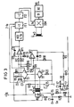
- the arrangement for carrier recovery shown in detail in FIG. 3 contains, in addition to the two emitter-coupled amplifiers formed from transistors T1 ... T4 and a fifth transistor T5 connected as a diode, a preamplifier stage containing a sixth transistor T6.
- the input E is connected via a first capacitor C1 to the base terminal of the sixth transistor T6, the base bias for this transistor is generated by means of a base voltage divider formed from a first and a second resistor R1, R2.
- the emitter connection of this transistor is connected to reference potential via the series circuit of a third and a fourth resistor, and the drain connection of a seventh transistor T7 for gain control is also connected to the third resistor R3.
- the collector terminal of the sixth transistor T6 is connected to one terminal of the primary winding of the transformer U, the other terminal of which is connected to the operating voltage + U B.
- a second capacitor C2 and a fifth resistor R5 are additionally connected in parallel to the primary winding.
- the center connection of the secondary winding of the transformer is connected on the one hand via a sixth resistor R6 to the operating voltage source + U B and on the other hand via a fifth transistor T5 connected as a diode with reference potential, so that the base voltage divider already shown in FIG. 2 for the first and the second Transistor T1, T2 results.
- the collector connections of these two transistors are connected to the combined emitter connections of the third and fourth transistors T3, T4 in accordance with FIG.
- the collector connections of these two transistors are connected to reference potential via a sixth or seventh capacitor C6, C7.
- the collector terminal of the third transistor T3 is also connected via a twelfth resistor R12 to the inverting input and the collector terminal of the fourth transistor T4 is connected via a thirteenth resistor R13 to the non-inverting input of a first operational amplifier OP1.
- the collector terminals of the two transistors T3, T4 are also connected to operating voltage + U B via a fourteenth or fifteenth resistor R14, R15 and connected to the non-inverting input of a second operational amplifier OP2 via a sixteenth or seventeenth resistor R16, R17.
- the inverting input of this second operational amplifier is connected via a tenth resistor R10 with reference potential, via an eleventh resistor R11 to the operating voltage + U B and via an eighth capacitor C8 to the output of the second operational amplifier OP2.
- This output connection is also connected via a filter element comprising a ninth resistor R9 and a fifth capacitor C5 and an eighth resistor R8 to the gate terminal of the seventh transistor T7, this gate terminal is also connected to the drain terminal via the series connection of a third capacitor C3 and a seventh resistor R7 connected to this transistor, the source connection of which is connected to reference potential via a fourth capacitor C4.
- the combined emitter connections of the first and second transistors T1, T2 are connected to reference potential via a twentieth resistor R20.
- the non-inverting input of the first operational amplifier is connected in series via a ninth capacitor C9 and an eighteenth resistor R18 with reference potential, while the inverting input of this operational amplifier is connected to the output of this operational amplifier via a tenth capacitor C10 and a nineteenth resistor R19.
- a voltage-coupled oscillator VCO is connected to this output, which generates an oscillation with a frequency corresponding to four times the carrier frequency 4 x fo.
- a first frequency divider FT1 with a divider ratio of 2: 1 is connected to the output connection of this oscillator, the two mutually complementary outputs of this frequency divider are connected to the base connection of the third and fourth transistor T3, T4 and lead these connections as shown in FIG.
- the 2 PSK signal is fed via the coupling capacitor C1 to the base connection of the amplifier transistor T6, in the collector circuit of which the bandpass already described lies.
- the bandwidth of this bandpass is set by the fifth resistor R5 so that it corresponds approximately to twice the clock frequency of the data signal with which the carrier was modulated.
- the center frequency of the bandpass corresponds to the frequency of the carrier fo.
- the combined phase-amplitude controller consists of transistors T1, T2 and T3, T4.
- the transistor T5 is connected as a diode to compensate for the threshold voltages of the transistors T1, T2. In the exemplary embodiment, these transistors T1 to T5 are monolithically integrated for reasons of lower offset.
- a current with twice the carrier frequency flows in the common emitter resistance of the transistors T1, T2 and in the common collector line.
- This current is switched between these two transistors by a square-wave differential voltage at the base connections of the third and fourth transistors T3, T4.
- the switching voltage required for this with the double carrier frequency 2fo is generated by the first frequency divider FT1, which is connected downstream of the controllable oscillator VCO. This generation by means of a frequency divider generates exactly symmetrical control voltages.
- the collector resistors R14, R15 of the transistors T3, T4 have the same resistance values and each form a low-pass filter with the capacitors C6, C7, which are also of the same size.
- the difference in the collector voltages of the transistors T3, T4 is proportional to the phase deviation between the switching voltage Us at the base terminals of the third and fourth transistors T3, T4 and the signal component contained in the combined collector current of the first and second transistors T1, T2 with twice the carrier frequency 2fo .
- the arrangement described thus represents the phase demodulator of the phase-locked loop for carrier recovery.
- the first operational amplifier OP1 forms the active loop filter of the phase-locked loop, in which the voltage difference between the collector voltages of the third and fourth transistors T3, T4 is converted into a control voltage for frequency control of the controllable oscillator VCO .
- the first operational amplifier OP1 is connected as a symmetry-asymmetry converter, so that only the difference in the collector voltages of the transistors T3, T4 is evaluated.
- the resistor pairs R12, R13 and R18, R19 are therefore each of the same size.
- the active loop filter formed by the first operational amplifier OP1 has a proportional-integral characteristic (PI behavior), so the static value of the voltage difference in the entire tracking range of the phase-locked loop must be 0, so that the relative phases position between the switching voltage Us and the input signal Ue remains constant in the locked state, as shown in FIG. 2b.
- PI behavior proportional-integral characteristic
- the edges of the switching voltage Us which are simultaneous with the zero crossings of the input signal can therefore be used to control a second frequency divider which generates the desired carrier frequency with the exact phase positions of 0 ° or 180 ° with respect to the 2 PSK signal.
- a binary signal is generated in the synchronous demodulator DEM, which is fed to the amplitude decider E via the low-pass filter TP and converted into a square-wave signal by the latter.
- the low-pass filter TP forms the entire selection with the input band-pass filter on the transmitter.
- the bandwidth of the input band-pass filter was chosen to be greater than the clock frequency by a factor of 2, so that practically the entire carrier-frequency selection is shifted to the low-pass filter TP. This results in the function of a tracking filter, the center frequency of which is always the same as the carrier frequency. The problem of detuning the center frequency of bandpasses with the resulting conversion of amplitudes into phase modulation therefore no longer occurs.
- the arithmetic mean value of the collector voltages is also important for the carrier recovery circuit described. This mean value is completely independent of the phase position between switching voltage Us and summation collector current of transistors T1, T2, but it is a direct measure of the input voltage and can therefore serve as a control criterion for level control on the input side.
- the second operational amplifier OP2 is provided, which receives a reference voltage at its inverting input via the voltage divider formed by the tenth and eleventh resistors R10, R11, and also receives a proportional voltage through the feedback from the output to the inverting input via the eighth capacitor C8. Has integral behavior.
- a control signal is emitted via a filter element to the gate electrode of the field effect transistor T7, which is switched on as a variable resistor in the emitter-side negative feedback of the preamplifier with the transistor T6.
- This circuit regulates the input level to that voltage value which corresponds to an average value of the voltage drops across the resistors R14 and R15 which is the same as the voltage drop across the eleventh resistor R11.
- the low-pass filter connected between the output of the second operational amplifier OP2 and the gate electrode of the field effect transistor T7 contains the eighth resistor R8, the value of which corresponds to that of the seventh resistor R7 in the connection between the gate and drain electrodes.
- the alternating current resistances of the third and fifth capacitors C3, C5 are small compared to the resistors R7 and R8, a superimposed alternating voltage component occurs on the gate electrode of the field effect transistor in addition to the controlling direct voltage, which because of the voltage divider effect between the equal-sized resistors R7 and R8 corresponds approximately to half the voltage between the drain and source electrode of the field effect transistor and considerably improves the distortion behavior of the field effect transistor actuator.
Landscapes
- Engineering & Computer Science (AREA)
- Computer Networks & Wireless Communication (AREA)
- Signal Processing (AREA)
- Digital Transmission Methods That Use Modulated Carrier Waves (AREA)
- Networks Using Active Elements (AREA)
- Apparatus For Radiation Diagnosis (AREA)
- Burglar Alarm Systems (AREA)
Description
- Die Erfindung betrifft eine Anordnung zur Trägerrückgewinnung entsprechend dem Oberbegriff des Patentanspruchs 1. Unter 2 PSK-Signalen werden dabei phasensprungmodulierte Signale verstanden, bei denen die Phasenlage eines Trägers nur die Werte von etwa 0° oder etwa 180° aufweist.
- Die Ubertragung von Signalen mittels Phasensprungmodulation ist seit langem bekannt. Die Übertragung digitaler Signale erfolgt in der Regel als 2 PSK- oder 4 PSK-Signal, wobei also die Phasenlage eines Trägers zwischen zwei oder vier diskreten Werten umgeschaltet wird. Handelt es sich bei dem digitalen Signal beispielsweise um ein Binärsignal mit einer angenäherten Gleichverteilung von logischen Einsen und logischen Nullen, so sind beim 2 PSK-Signal die Phasenlagen des Trägers von 0° und 180° annähernd gleichhäufig vertreten, so daß die Amplitude des Trägers nahezu Null ist. Es ist aber bekannt, daß die Demodulation eines 2 PSK-Signales in einem gestörten Kanal bezüglich des Signal-Geräuschabstandes bzw. der Bitfehlerrate des rückgewonnen Binärsignals nur dann optimal sein kann, wenn für die Demodulation ein Synchrondemodulator mit phasenrichtig zugeführtem Träger verwendet wird. Damit ergibt sich die Notwendigkeit, aus dem empfangenen PSK-Signal den Träger zurückzugewinnen.
- In der Fig. 1 ist eine bekannte Anordnung zur Trägerrückgewinnung für ein 2 PSK-Signal dargestellt. Empfangsseitig ist zunächst ein Bandpaß BP angeordnet, dessen Ah 1 Or/02.10.1984 Mittenfrequenz gleich der Trägerfrequenz und dessen Bandbreite mindestens zweimal der Taktfrequenz bzw. der Nyquistfrequenz des Binärsignals ist. Das Ausgangssignal des Bandpasses wird zum einen dem Signaleingang eines Synchrondemodulators DEM und zum anderen dem Eingang eines Doppelweggleichrichters oder Quadrierers 0 zugeführt. Bei der Quadrierung wird das vorgefilterte 2 PSK-Signal mit sich selbst multipliziert, dabei entstehen auch Summenfrequenzen aller spektralen Anteile im oberen und unteren Seitenband. Die Anteile, die symmetrisch zum unterdrückten Träger liegen, treten bei der doppelten Trägerfrequenz auf, sie addieren sich wegen der Korrelation des oberen und des unteren Seitenbandes. Diese Energieanteile bei der doppelten Trägerfrequenz werden in einem schmalbandigen Trägerfrequenzfilter F von den bei der Quadrierung entstandenen unerwünschten Mischprodukten weitgehend befreit und an einen nachgeschalteten Amplitudenbegrenzer abgegeben. Nach der Amplitudenbegrenzung erfolgt in einem Frequenzteiler im Teilungsverhältnis 2:1 die Erzeugung des Trägers, der an den Trägereingang des Synchrondemodulators DEM abgegeben wird. Im Synchrondemodulator erfolgt die Demodulation des 2 PSK-Eingangssignals, an dem Demodulatorausgang ist über einen Tiefpaß ein Amplitudenentscheider AE angeschlossen, von dem ein binäres Signal BS abgegeben wird.
- Im Synchrondemodulator wird eine Multiplikation des empfangsseitig rückgewonnenen Trägers mit dem Signal vorgenommen, eine optimale Demodulation des 2 PSK-Signals mit maximalem Signal-Geräuschabstand ergibt sich nur bei richtiger Phasenlage des zurrückgewonnenen Träger. Da die Phase des rückgewonnenen Trägers bei allen Trägerrückgewinnungsschaltungen für 2 PSK-Signale wegen der Ableitung aus der Korrelation der Signalseitenbänder bzw. wegen der 2:1 Frequenzteilung 0° oder 180° betragen kann ist der erzeugte Träger mit dieser Unsicherheit behaftet. Bei der Übertragung von 2 PSK-Signalen wird zur Umgehung dieser Unsicherheit deshalb in der Regel als modulierendes Binärsignal ein Signal im Differenz-Binärcode verwendet, bei dem die Information in den Signalwechseln übertragen wird.
- Aus der US-A-2167 408 ist bereits ein Synchrondemodulator für 2 PSK-Signale mit einer Anordnung zurTrägerrückgewinnung bekannt, die einen eingangsseitigen Bandpaß mit einstellbarer Phase zur Phasenkorrektur und diesem nachgeschaltet einen Frequenzverdoppler mit angeschlossenem Phasendiskriminator enthält. Durch den Phasendiskriminator wird die Temperatur von 2 Schwingquarzen verändert, die jeweils in einem quarzstabilisierten Oszillator angeordnet sind. Die Ausgangssignale der beiden Oszillatoren ergeben durch Mischung eine Differenzfrequenz die der gewünschten Trägerfrequenz entspricht. Die Ausgangssignale der beiden Oszillatoren werden dazu einer Gegentaktstufe zugeführt, die zusätzlich ein die zweite Harmonische der Trägerfrequenz enthaltendes Ausgangssignal des Phasendiskriminators zur phasenmäßigen Synchronisierung des erzeugten Trägerfrequenzsignals erhält.
- Beim bekannten Stand der Technik ergibt sich ein vergleichsweise hoher Aufwand für die Trägerrückgewinnung, da hierfür unter anderem Filter benötigt werden, die hinsichtlich Phasenstabilität des rückgewonnenen Trägers bei gleichzeitig hoher Selektion hohe Temperatur- und Alterungsbeständigkeit aufweisen müssen.
- Die Aufgabe der Erfindung besteht also darin, eine gegenüber dem Stande der Technik vereinfachte Anordnung zur Trägerrückgewinnung aus empfangenen 2 PSK-Signalen zu finden.
- Erfindungsgemäß wird die Aufgabe durch eine Anordnung der eingangs erwähnten Art gelöst, die durch die Merkmale entsprechend dem Kennzeichen des Patentanspruchs 1 weitergebildet ist. Der Vorteil der erfindungsgemäßen Anordnung liegt insbesondere darin, daß die Quadrierung des 2 PSK-Eingangssignales, eine offsetfreie Phasenregelung und eine Amplitudenregelung von einer einzigen Anordnung vorgenommen werden, die als kombinierter Phasen-Amplituden-Vergleicher wirkt und eine Phasenregelschleife darstellt. Vorteilhafte Weiterbildungen der erfindungsgemäßen Anordnung sind in den Patentansprüchen 2-4 beschrieben.
- Die Erfindung soll im folgenden anhand der Zeichnung näher erläutert werden.
- In der Zeichnung zeigt
- Fig. 1 eine bekannte Anordnung zur Demodulation von 2 PSK-Signalen mit einer Anordnung zur Trägerrückgewinnung,
- Fig. 2 die Prinzipschaltung der erfindungsgemäßen Anordnung zur Trägerrückgewinnung mit einem Phasendiagramm und
- Fig. 3 eine detaillierte Schaltung der erfindungsgemäßen Anordnung zur Trägerrückgewinnung.
- In der Fig. 2a ist in einer Prinzipschaltung ein Teil der erfindungsgemäßen Anordnung zur Trägerrückgewinnung dargestellt. Mit einem Eingang E für das Eingangssignal sind die beiden Primärwicklungsanschlüsse eines Übertragers Ü sowie die beiden Anschlüsse eines Kondensators CO verbunden. In Verbindung mit dem Kondensator wirkt die Induktivität des Übertragers Ü als Bandpaß, die Sekundärwicklung dieses Übertragers ist mittelangezapft, die Mittelanzapfung ist mit einem Basisspannungsteiler verbunden, der durch einen an die Betriebsspannung +UB angeschlossenen Widerstand RO und eine mit Bezugspotential verbundene Diode D gebildet wird. Die beiden äußeren Anschlüsse der Sekundärwicklung des Übertragers Ü sind jeweils mit einem Basisanschluß eines ersten bzw. zweiten Transistors T1, T2 verbunden, deren Emitteranschlüsse miteinander und über einen Widerstand RE mit Bezugspotential verbunden sind. Die beiden Transistoren, deren Schwellenspannung durch die Diode D kompensiert wird, werden also im Gegentakt angesteuert. Da die Kollektöranschlüsse beider Transistoren miteinander verbunden sind, ergibt sich ein Kollektorsummenstrom lo der dem Absolutwert der Eingangsspannung und dem Kehrwert des Widerstandes RE proportional ist. Damit liegt bereits eine Doppelweggleichrichtung für das Signal am Eingang E vor. Durch die Doppelweggleichrichtung ergibt sich hinsichtlich der Welligkeit des Stromes lo die doppelte Frequenz gegenüber der des Eingangssignals, es liegt also ein Signal mit der doppelten Trägerfrequenz vor, so daß die Quadriererfunktion bereits realisiert ist. Mit den verbundenen Kollektoranschlüssen der beiden Transistoren T1 und T2 sind die Emitteranschlüsse eines dritten und eines vierten Transistors T3, T4 verbunden, den Basisanschlüssen beider Transistoren wird eine zueinander um 180° phasenverschobene symmetrische Rechteckspannung Us mit der doppelten Trägerfrequenz zugeführt. Durch diese Rechteckspannung wird der dritte und der vierte Transistor T3, T4 umgeschaltet, so daß über die Kollektoranschlüsse dieser Transistoren zueinander phasenverschobene Ströme 11, 12 fließen. Die Differenz der Mittelwerte dieser Ströme ist dabei eine Funktion der Phasenverschiebung zwischen der Komponente mit der doppelten Trägerfrequenz im zusammengefaßten Kollektorstrom lo der ersten beiden Transistoren T1, T2 und der Rechteckspannung Us.
- In der Fig. 2b sind übereinander die Eingangsspannung Ue, der Kollektorsummenstrom lo der beiden ersten Transistoren und die dem dritten und vierten Transistor T3, T4 umschaltender Rechteckspannung Us dargestellt.
- In der Zeichnung ist die Phase der Rechteckspannung Us im Hinblick auf die Phase des Grundwellenanteils im Summenstrom lo um 90° verschoben, die Differenz der Gleichstrommittelwerte der Kollektorströme 11, 12 des dritten und des vierten Transistors T3, T4 ist hierbei gleich Null. Die Differenz der Kollektorströme 11, 12 der beiden Transistoren T3, T4 ist ein Ausdruck der Phasenlage zwischen Rechteckspannung Us und Eingangsspannung Ue mit angenäherter Sinuscharakteristik und kann als Regelkriterium in einer Phasenregelschleife verwendet werden, außerdem ist aber die Summe dieser beiden Ströme gleich dem Summenstrom lo, dessen Gleichstrommittelwert der Eingangsspannung Ue proportional ist und sich damit als Regelkriterium für eine eingangsseitige Amplitudenregelung anbietet.
- Die in der Fig. 3 detailliert dargestellte Anordnung zur Trägerrückgewinnnung enthält neben den beiden, aus den Transistoren T1 ... T4 gebildeten emittergekoppelten Verstärkern und einem als Diode geschalteten fünften Transistor T5 eine, einen sechsten Transistor T6 enthaltende Vorverstärkerstufe. Der Eingang E ist über einen ersten Kondensator C1 mit dem Basisanschluß des sechsten Transistors T6 verbunden, die Basisvorspannung wird für diesen Transistor mittels eines aus einem ersten und einem zweiten Widerstand R1, R2 gebildeten Basisspannungsteilers erzeugt. Der Emitteranschluß dieses Transistors ist über die Reihenschaltung eines dritten und eines vierten Widerstandes mit Bezugspotential verbunden, außerdem ist am dritten Widerstand R3 der Drainanschluß eines siebenten Transistors T7 zur Verstärkungsregelung angeschlossen. Der Kollektoranschluß des sechsten Transistors T6 ist mit dem einen Anschluß der Primärwicklung des Übertragers Ü verbunden, deren anderer Anschluß an die Betriebsspannung +UB angeschlossen ist. Der Primärwicklung ist zusätzlich ein zweiter Kondensator C2 und ein fünfter Widerstand R5 parallelgeschaltet. Der Mittelanschluß der Sekundärwicklung des Übertragers ist einerseits über einen sechsten Widerstand R6 mit der Betriebsspannungsquelle +UB und andererseits über einen als Diode geschalteten fünften Transistor T5 mit Bezugspotential verbunden, so daß sich der in Fig. 2 bereits dargestellte Basisspannungsteiler für den ersten und den zweiten Transistor T1, T2 ergibt. Die Kollektoranschlüsse dieser beiden Transistoren sind entsprechend der Fig. 2a mit den zusammengefaßten Emitteranschlüssen des dritten und des vierten Transistors T3, T4 verbunden, die Kollektoranschlüsse dieser beiden Transistoren sind über einen sechsten bzw. siebten Kondensator C6, C7 mit Bezugspotential verbunden. Der Kollektoranschluß des dritten Transistors T3 ist außerdem über einen zwölften Widerstand R12 mit dem invertierenden Eingang und der Kollektoranschluß des vierten Transistors T4 ist über einen dreizehnten Widerstand R13 mit dem nichtinvertierenden Eingang einers ersten Operationsverstärkers OP1 verbunden. Die Kolektoranschlüsse der beiden Transistoren T3, T4 sind ausserdem über einen vierzehnten bzw. fünfzehnten Widerstand R14, R15 an Betriebsspannung +UB angeschlossen und über einen sechzehnten bzw. siebzehnten Widerstand R16, R17 mit dem nichtinvertierenden Eingang eines zweiten Operationsverstärkers OP2 verbunden. Der invertierende Eingang dieses zweiten Operationsverstärkers ist über einen zehnten Widerstand R10 mit Bezugspotential, über einen elften Widerstand R11 mit der Betriebsspannung +UB sowie über einen achten Kondensator C8 mit dem Ausgang des zweiten Operationsverstärkers OP2 verbunden. Dieser Ausgangsanschluß ist ausserdem über ein Siebglied aus einem neunten Widerstand R9 und einen fünften Kondensator C5 sowie einem achtem Widerstand R8 mit dem Gateanschluß des siebten Transistors T7 verbunden, dieser Gateanschluß ist außerdem über die Reihenschaltung eines dritten Kondensators C3 und eines siebten Widerstands R7 mit dem Drainanschluß dieses Transistors verbunden, dessen Sourceanschluß über einen vierten Kondensator C4 mit Bezugspotential verbunden ist. Die zusammengefaßten Emitteranschlüsse des ersten, des zweiten Transistor T1, T2 sind über einen zwanzigsten Widerstand R20 mit Bezugspotential verbunden.
- Der nichtinvertierende Eingang des ersten Operationsverstärkers ist über die Reihenschaltung eines neunten Kondensators C9 und eines achzehnten Widerstandes R18 mit Bezugspotential verbunden, während der invertierende Eingang dieses Operationsverstärkers über einen zehnten Kondensator C10 und einen neunzehnten Widerstand R19 mit dem Ausgang dieses Operationsverstärkers verbunden ist. An diesen Ausgang ist ein spannungsgekoppelter Oszillator VCO angeschlossen, der eine Schwingung mit einer Frequenz entsprechend der vierfachen Trägerfrequenz 4 x fo erzeugt. An den Ausgangsanschluß dieses Oszillators ist ein erster Frequenzteiler FT1 mit einem Teilerverhältnis von 2:1 angeschlossen, die beiden zueinander komplementären Ausgänge dieses Frequenzteilers sind mit den Basisanschluß des dritten bzw. des vierten Transistors T3, T4 verbunden und führen diesen Anschlüssen die in der Fig. 2 dargestellte Rechteckspannung Us mit einer Frequenz entsprechend der doppelten Trägerfrequenz zu. Mit einem Ausgangsanschluß dieses Frequenzteilers ist weiterhin der Eingang eines zweiten Frequenzteilers FT2 verbunden, dieser Frequenzteiler mit einem Teilerverhältnis von 2:1 erzeugt den gewünschten Träger, seine beiden komplementären Ausgänge sind mit zugeordneten Eingängen des Synchrondemodulators DEM entsprechend der Fig. 1 verbunden, außerdem sind die Signaleingänge dieses Demodulators mit Anschlüssen einer weiteren Sekundärwicklung w3 des Übertragers Ü verbunden. An den Demodulator DEM schließen sich der Tiefpaß TP und der Amplitudenentscheider AE entsprechend der Fig. 1 an.
- Die Wirkungsweise der Anordnung zur Trägerrückgewinnung ist im Prinzip anhand der Fig. 2 erläutert, nachfolgend soll auf Details eingegangen werden. Das 2 PSK-Signal wird über den Koppelkondensator C1 den Basisanschluß des Verstärkertransistors T6 zugeführt, in dessen Kollektorkreis der schon beschriebene Bandpaß liegt. Die Bandbreite dieses Bandpasses wird durch den fünften Widerstand R5 so eingestellt, daß sie etwa der doppelten Taktfrequenz des Datensignals entspricht, mit dem der Träger moduliert wurde. Die Mittenfrequenz des Bandpasses entspricht der Frequenz des Trägers fo. Der kombinierte Phasen-Amplitudenregler besteht entsprechend der Fig. 2 aus den Transistoren T1, T2 sowie T3, T4. Der Transistor T5 ist zur Kompensation der Schwellenspannungen der Transistoren T1, T2 als Diode geschaltet. Diese Transistoren T1 bis T5 sind beim Ausführungsbeispiel aus Gründen des geringeren Offsets gemeinsam monolithisch integriert.
- Wie bereits in Verbindung mit Fig. 2 beschrieben, fließt im gemeinsamen Emitterwiderstand der Transistoren T1, T2 sowie in der gemeinsamen Kollektorleitung ein Strom mit der doppelten Trägerfrequenz. Dieser Strom wird durch eine Rechteckdifferenzspannung an den Basisanschlüssen des dritten und des vierten Transistors T3, T4 zwischen diesen beiden Transistoren umgeschaltet. Die dafür benötigte Umschaltspannung mit der doppelten Trägerfrequenz 2fo wird vom ersten Frequenzteiler FT1 erzeugt, der dem steuerbaren Oszillator VCO nachgeschaltet ist. Durch diese Erzeugung mittels Frequenzteiler werden exakt symmetrische Ansteuerungsspannungen erzeugt. Die Kollektorwiderstände R14, R15 der Transistoren T3, T4 haben gleiche Widerstandswerte und bilden mit den ebenfalls gleich großen Kondensatoren C6, C7 jeweils einen Tiefpaß. Die Differenz der Kollektorspannungen der Transistoren T3, T4 ist proportional der Phasenabweichung zwischen der Umschaltspannung Us an den Basisanschlüssen des dritten und des vierten Transistors T3, T4 und der im zusammengefaßten Kollektorstrom des ersten und des zweiten Transistors T1, T2 enthaltenen Signalkomponente mit der doppelten Trägerfrequenz 2fo. Damit stellt die beschriebene Anordnung den Phasendemodulator der Phasenregelschleife zur Trägerrückgewinnung dar. Der erste Operationsverstärker OP1 bildet das aktive Schleifenfilter der Phasenregelschleife, in dem die Spannungsdifferenz der Kollektorspannungen des dritten und des vierten Transistors T3, T4 in eine Steuerspannung zur Frequenzregelung des steuerbaren Oszillators VCO umgeformt wird. Der erste Operationsverstärker OP1 ist dabei als Symmetrie-Unsymmetriewandler beschaltet, so daß nur die Differenz der Kollektorspannungen der Transistoren T3, T4 ausgewertet wird. Neben dem Kondensatorpaar C9, C10 sind deshalb auch die Widerstandspaare R12, R13 sowie R18, R19 jeweils gleich groß dimensioniert.
- Das durch den ersten Operationsverstärker OP1 gebildete aktive Schleifenfilter besitzt eine Proportional-Integral Charakteristik (PI-Verhalten), damit muß der statische Wert der Spannungsdifferenz im gesamten Nachführbereich der Phasenregelschleife 0 sein, so daß die relative Phasenlage zwischen der Schaltspannung Us und dem Eingangssignal Ue im eingerasteten Zustand konstant bleibt, so wie dies in Fig. 2b dargestellt ist. Die mit den Nulldurchgängen des Eingangssignals zeitgleichen Flanken der Umschaltspannung Us können deshalb zur Ansteuerung eines zweiten Frequenzteilers verwendet werden, der die gewünschte Trägerfrequenz mit den exakten Phasenlagen von 0° oder 180° in Bezug auf das 2 PSK-Signal erzeugt.
- Durch Multiplikation des verstärkten Eingangssignals und des rückgewonnenen Trägers wird im Synchrondemodulator DEM ein binäres Signal erzeugt, daß über den Tiefpaß TP dem Amplitudenentscheider E zugeführt und von diesem in ein Rechtecksignal umgeformt wird. Der Tiefpaß TP bildet dabei mit dem Eingangsbandpaß am Übertrager die gesamte Selektion beim Ausführungsbeispiel wurde die Bandbreite des Eingangsbandpasses um den Faktor 2 größer als die Taktfrequenz gewählt, so daß Praktisch die gesamte trägerfrequente Selektion in den Tiefpaß TP verlagert wird. Dadurch ergibt sich die Funktion eines Nachlauffilters (tracking filter), dessen Mittenfrequenz immer gleich der Trägerfrequenz ist. Damit tritt das Problem einer Verstimmung der Mittenfrequenz von Bandpässen mit der daraus resultierenden Umwandlung von Amplituden in Phasenmodulation nicht mehr auf.
- Neben der Differenz der Kollektorspannungen der Transistoren T3, T4 ist für die beschriebene Trägerrückgewinnungsschaltung auch der arithmetische Mittelwert der Kollektorspannungen von Bedeutung. Dieser Mittelwert ist von der Phasenlage zwischen Schaltspannung Us und Summkollektorstrom der Transistoren T1, T2 vollständig unabhängig, er ist jedoch ein direktes Maß für die Eingangsspannung und kann damit als Regelkriterium für eine eingangsseitige Pegelregelung dienen. Zur Pegelregelung ist der zweite Operationsverstärker OP2 vorgesehen, der an seinem invertierenden Eingang über den aus den zehnten und den elften Widerstand R10, R11 gebildeten Spannungsteiler eine Referenzspannung erhält und durch die Rückkopplung vom Ausgang auf den invertierenden Eingang über den achten Kondensator C8 ebenfalls ein Proportional-Integral Verhalten aufweist. Vom Ausgang des zweiten Operationsverstärkers OP2 wird ein Steuersignal über ein Siebglied an die Gateelektrode des Feldeffekttransistors T7 abgegeben, der als Stellwiderstand in der emitterseitigen Gegenkopplung des Vorverstärkers mit dem Transistor T6 eingeschaltet ist. Durch diese Schaltung wird der Eingangspegel auf denjenigen Spannungswert geregelt, der einem dem Spannungsabfall am elften Widerstand R11 gleichgroßen Mittelwert der Spannungsabfälle an den Widerständen R14 bzw. R15 entspricht.
- Der zwischen dem Ausgang des zweiten Operationsverstärkers OP2 und der Gateelektrode des Feldeffekttransistors T7 eingeschaltete Tiefpaß enthält den achten Widerstand R8, dessen Wert dem des siebten Widerstandes R7 in der Verbindung zwischen Gate- und Drainelektrode entspricht. Unter der Voraussetzung, daß die Wechselstromwiderstände des dritten und des fünften Kondensators C3, C5 klein gegenüber den Widerständen R7 und R8 sind, tritt an der Gateelektrode des Feldeffekttransistors neben der steuerenden Gleichspannung ein überlagerter Wechselspannungsanteil auf, der wegen des Spannungsteilereffektes zwischen den gleichgroßen Widerständen R7 und R8 etwa der halben Spannung zwischen Drain und Sourceelektrode des Feldeffekttransistors entspricht und das Klirrverhalten des Feldeffekttransistor-Stellgliedes erheblich verbessert.
Claims (4)
Priority Applications (1)
| Application Number | Priority Date | Filing Date | Title |
|---|---|---|---|
| AT85112423T ATE54788T1 (de) | 1984-10-04 | 1985-10-01 | Anordnung zur traegerrueckgewinnung aus empfangenen 2 psk-signalen. |
Applications Claiming Priority (2)
| Application Number | Priority Date | Filing Date | Title |
|---|---|---|---|
| DE3436436 | 1984-10-04 | ||
| DE3436436 | 1984-10-04 |
Publications (2)
| Publication Number | Publication Date |
|---|---|
| EP0177883A1 EP0177883A1 (de) | 1986-04-16 |
| EP0177883B1 true EP0177883B1 (de) | 1990-07-18 |
Family
ID=6247098
Family Applications (1)
| Application Number | Title | Priority Date | Filing Date |
|---|---|---|---|
| EP85112423A Expired - Lifetime EP0177883B1 (de) | 1984-10-04 | 1985-10-01 | Anordnung zur Trägerrückgewinnung aus empfangenen 2 PSK-Signalen |
Country Status (4)
| Country | Link |
|---|---|
| US (1) | US4675883A (de) |
| EP (1) | EP0177883B1 (de) |
| AT (1) | ATE54788T1 (de) |
| DE (1) | DE3578725D1 (de) |
Families Citing this family (2)
| Publication number | Priority date | Publication date | Assignee | Title |
|---|---|---|---|---|
| US4835493A (en) * | 1987-10-19 | 1989-05-30 | Hughes Aircraft Company | Very wide bandwidth linear amplitude modulation of RF signal by vector summation |
| DE19614979C2 (de) | 1995-04-20 | 2001-05-17 | Fujitsu Ltd | Hochfrequenz-Sende-Empfangs-Vorrichtung zur Datenkommunikation |
Family Cites Families (12)
| Publication number | Priority date | Publication date | Assignee | Title |
|---|---|---|---|---|
| US2167480A (en) * | 1927-11-02 | 1939-07-25 | Rca Corp | Signaling |
| US3339143A (en) * | 1959-07-17 | 1967-08-29 | Ralph G Lucas | Selective receiver for communication by phase shift |
| US3349330A (en) * | 1964-03-18 | 1967-10-24 | Automatic Elect Lab | Diphase transceiver with modulatordemodulator isolation |
| GB1353017A (en) * | 1970-04-21 | 1974-05-15 | Xerox Corp | Data-transmission systems |
| DE2065287C1 (de) * | 1970-09-30 | 1977-12-08 | Siemens Ag, 1000 Berlin Und 8000 Muenchen | Schaltung |
| US3753114A (en) * | 1971-12-02 | 1973-08-14 | Culbertson Ind Inc | Method and apparatus for the recovery of synchronous carrier in a digital communication system |
| NL7705842A (nl) * | 1977-05-27 | 1978-11-29 | Bell Telephone Mfg | Inrichting voor het onttrekken van een klokpuls- reeks aan een ingangspulsreeks. |
| US4233565A (en) * | 1979-06-29 | 1980-11-11 | Motorola, Inc. | Method and apparatus for a PSK signal detector |
| US4298986A (en) * | 1979-12-26 | 1981-11-03 | General Electric Company | Receiver for phase-shift modulated carrier signals |
| FR2502872B1 (fr) * | 1981-03-27 | 1988-06-17 | Laures Antoine | Organe de recuperation de porteuse pour signal a modulations mdp2 ou mdp4 |
| JPS58114654A (ja) * | 1981-12-28 | 1983-07-08 | Fujitsu Ltd | 基準搬送波再生回路 |
| US4540948A (en) * | 1982-09-14 | 1985-09-10 | Nec Corporation | 8-Phase phase-shift keying demodulator |
-
1985
- 1985-09-27 US US06/780,894 patent/US4675883A/en not_active Expired - Fee Related
- 1985-10-01 EP EP85112423A patent/EP0177883B1/de not_active Expired - Lifetime
- 1985-10-01 AT AT85112423T patent/ATE54788T1/de not_active IP Right Cessation
- 1985-10-01 DE DE8585112423T patent/DE3578725D1/de not_active Expired - Lifetime
Also Published As
| Publication number | Publication date |
|---|---|
| US4675883A (en) | 1987-06-23 |
| EP0177883A1 (de) | 1986-04-16 |
| DE3578725D1 (de) | 1990-08-23 |
| ATE54788T1 (de) | 1990-08-15 |
Similar Documents
| Publication | Publication Date | Title |
|---|---|---|
| DE3713821C2 (de) | Trennverstärker mit genauer Zeitlage der über die Isolationsbarriere gekoppelten Signale | |
| EP0401771A2 (de) | Schaltungsanordnung zur Frequenzumsetzung | |
| EP0209188B1 (de) | Getakteter Gleichspannungswandler | |
| EP0177883B1 (de) | Anordnung zur Trägerrückgewinnung aus empfangenen 2 PSK-Signalen | |
| EP0614587B1 (de) | Demodulationsverfahren mit anwendung einer quadraturmodulation | |
| DE2831091C2 (de) | Frequenzdemodulator mit einer Phasennachführschleife | |
| DE1906957C3 (de) | Demodulatorverstärker für winkelmodulierte elektrische Hochfrequenzschwingungen | |
| DE2754268C2 (de) | Verstärker für ein impulsbreitenmoduliertes Signal | |
| DE68911801T2 (de) | 50 Prozent-Präzisionstastverhältnisregler. | |
| DE1806905C3 (de) | Impulsformerschaltung | |
| DE4220296A1 (de) | Schaltungsanordnung zur Unterdrückung schmalbandiger Störsignale | |
| DE869358C (de) | Schaltungsanordnung zur Frequenzmodulation einer elektrischen Schwingung | |
| DE635535C (de) | Anordnung zur Frequenzregelung bei Empfaengern | |
| DE1591424C2 (de) | Schaltung zur Demodulation einer winkelmodulierten Trägerschwingung | |
| DE69604111T2 (de) | FM-Demodulator | |
| DE3114761C2 (de) | ||
| DE60203160T2 (de) | Quadratur-modulator und demodulator | |
| DE3839090C2 (de) | ||
| DE809669C (de) | Schaltung zur Demodulation frequenzmodulierter Schwingungen | |
| EP0123333B1 (de) | Verfahren zur Erzeugung eines annähernd sinusförmigen Signals und Schaltungsanordnung zur Durchführung dieses Verfahrens, insbesondere für einen Stereo-Demodulator | |
| DE1962197A1 (de) | Datenuebertragungsanlage | |
| DE2900599C2 (de) | Verfahren und Anordnung zur Regenerierung des zur Übertragung verwendeten Hauptenergiebereichs eines trägerfrequenten digitalen Signals | |
| DE3304181A1 (de) | Afc-abstimmschaltung | |
| DE3223904A1 (de) | Filter- und demodulationsschaltung | |
| DE19643833C1 (de) | Verfahren zur Demodulation |
Legal Events
| Date | Code | Title | Description |
|---|---|---|---|
| PUAI | Public reference made under article 153(3) epc to a published international application that has entered the european phase |
Free format text: ORIGINAL CODE: 0009012 |
|
| AK | Designated contracting states |
Kind code of ref document: A1 Designated state(s): AT BE CH DE FR GB IT LI NL SE |
|
| 17P | Request for examination filed |
Effective date: 19860923 |
|
| 17Q | First examination report despatched |
Effective date: 19890619 |
|
| GRAA | (expected) grant |
Free format text: ORIGINAL CODE: 0009210 |
|
| AK | Designated contracting states |
Kind code of ref document: B1 Designated state(s): AT BE CH DE FR GB IT LI NL SE |
|
| PG25 | Lapsed in a contracting state [announced via postgrant information from national office to epo] |
Ref country code: SE Effective date: 19900718 Ref country code: IT Free format text: LAPSE BECAUSE OF FAILURE TO SUBMIT A TRANSLATION OF THE DESCRIPTION OR TO PAY THE FEE WITHIN THE PRESCRIBED TIME-LIMIT;WARNING: LAPSES OF ITALIAN PATENTS WITH EFFECTIVE DATE BEFORE 2007 MAY HAVE OCCURRED AT ANY TIME BEFORE 2007. THE CORRECT EFFECTIVE DATE MAY BE DIFFERENT FROM THE ONE RECORDED. Effective date: 19900718 Ref country code: GB Effective date: 19900718 Ref country code: FR Effective date: 19900718 |
|
| REF | Corresponds to: |
Ref document number: 54788 Country of ref document: AT Date of ref document: 19900815 Kind code of ref document: T |
|
| REF | Corresponds to: |
Ref document number: 3578725 Country of ref document: DE Date of ref document: 19900823 |
|
| EN | Fr: translation not filed | ||
| GBV | Gb: ep patent (uk) treated as always having been void in accordance with gb section 77(7)/1977 [no translation filed] | ||
| PLBE | No opposition filed within time limit |
Free format text: ORIGINAL CODE: 0009261 |
|
| STAA | Information on the status of an ep patent application or granted ep patent |
Free format text: STATUS: NO OPPOSITION FILED WITHIN TIME LIMIT |
|
| 26N | No opposition filed | ||
| PGFP | Annual fee paid to national office [announced via postgrant information from national office to epo] |
Ref country code: BE Payment date: 19911023 Year of fee payment: 7 |
|
| PGFP | Annual fee paid to national office [announced via postgrant information from national office to epo] |
Ref country code: NL Payment date: 19911031 Year of fee payment: 7 |
|
| PG25 | Lapsed in a contracting state [announced via postgrant information from national office to epo] |
Ref country code: BE Effective date: 19921031 |
|
| BERE | Be: lapsed |
Owner name: SIEMENS A.G. Effective date: 19921031 |
|
| PG25 | Lapsed in a contracting state [announced via postgrant information from national office to epo] |
Ref country code: NL Effective date: 19930501 |
|
| NLV4 | Nl: lapsed or anulled due to non-payment of the annual fee | ||
| PGFP | Annual fee paid to national office [announced via postgrant information from national office to epo] |
Ref country code: AT Payment date: 19930929 Year of fee payment: 9 |
|
| PGFP | Annual fee paid to national office [announced via postgrant information from national office to epo] |
Ref country code: DE Payment date: 19931216 Year of fee payment: 9 |
|
| PGFP | Annual fee paid to national office [announced via postgrant information from national office to epo] |
Ref country code: CH Payment date: 19940118 Year of fee payment: 9 |
|
| PG25 | Lapsed in a contracting state [announced via postgrant information from national office to epo] |
Ref country code: AT Effective date: 19941001 |
|
| PG25 | Lapsed in a contracting state [announced via postgrant information from national office to epo] |
Ref country code: LI Effective date: 19941031 Ref country code: CH Effective date: 19941031 |
|
| REG | Reference to a national code |
Ref country code: CH Ref legal event code: PL |
|
| PG25 | Lapsed in a contracting state [announced via postgrant information from national office to epo] |
Ref country code: DE Effective date: 19950701 |