EP0177948A2 - Boîtier miniature pour circuit intégré - Google Patents
Boîtier miniature pour circuit intégré Download PDFInfo
- Publication number
- EP0177948A2 EP0177948A2 EP85112798A EP85112798A EP0177948A2 EP 0177948 A2 EP0177948 A2 EP 0177948A2 EP 85112798 A EP85112798 A EP 85112798A EP 85112798 A EP85112798 A EP 85112798A EP 0177948 A2 EP0177948 A2 EP 0177948A2
- Authority
- EP
- European Patent Office
- Prior art keywords
- lead
- cover
- integrated circuit
- base
- ins
- Prior art date
- Legal status (The legal status is an assumption and is not a legal conclusion. Google has not performed a legal analysis and makes no representation as to the accuracy of the status listed.)
- Withdrawn
Links
Images
Classifications
-
- H—ELECTRICITY
- H10—SEMICONDUCTOR DEVICES; ELECTRIC SOLID-STATE DEVICES NOT OTHERWISE PROVIDED FOR
- H10W—GENERIC PACKAGES, INTERCONNECTIONS, CONNECTORS OR OTHER CONSTRUCTIONAL DETAILS OF DEVICES COVERED BY CLASS H10
- H10W76/00—Containers; Fillings or auxiliary members therefor; Seals
- H10W76/60—Seals
-
- H—ELECTRICITY
- H10—SEMICONDUCTOR DEVICES; ELECTRIC SOLID-STATE DEVICES NOT OTHERWISE PROVIDED FOR
- H10W—GENERIC PACKAGES, INTERCONNECTIONS, CONNECTORS OR OTHER CONSTRUCTIONAL DETAILS OF DEVICES COVERED BY CLASS H10
- H10W72/00—Interconnections or connectors in packages
- H10W72/071—Connecting or disconnecting
-
- H—ELECTRICITY
- H10—SEMICONDUCTOR DEVICES; ELECTRIC SOLID-STATE DEVICES NOT OTHERWISE PROVIDED FOR
- H10W—GENERIC PACKAGES, INTERCONNECTIONS, CONNECTORS OR OTHER CONSTRUCTIONAL DETAILS OF DEVICES COVERED BY CLASS H10
- H10W76/00—Containers; Fillings or auxiliary members therefor; Seals
- H10W76/10—Containers or parts thereof
- H10W76/12—Containers or parts thereof characterised by their shape
-
- H—ELECTRICITY
- H10—SEMICONDUCTOR DEVICES; ELECTRIC SOLID-STATE DEVICES NOT OTHERWISE PROVIDED FOR
- H10W—GENERIC PACKAGES, INTERCONNECTIONS, CONNECTORS OR OTHER CONSTRUCTIONAL DETAILS OF DEVICES COVERED BY CLASS H10
- H10W76/00—Containers; Fillings or auxiliary members therefor; Seals
- H10W76/10—Containers or parts thereof
- H10W76/17—Containers or parts thereof characterised by their materials
- H10W76/18—Insulating materials, e.g. resins, glasses or ceramics
-
- Y—GENERAL TAGGING OF NEW TECHNOLOGICAL DEVELOPMENTS; GENERAL TAGGING OF CROSS-SECTIONAL TECHNOLOGIES SPANNING OVER SEVERAL SECTIONS OF THE IPC; TECHNICAL SUBJECTS COVERED BY FORMER USPC CROSS-REFERENCE ART COLLECTIONS [XRACs] AND DIGESTS
- Y10—TECHNICAL SUBJECTS COVERED BY FORMER USPC
- Y10T—TECHNICAL SUBJECTS COVERED BY FORMER US CLASSIFICATION
- Y10T29/00—Metal working
- Y10T29/49—Method of mechanical manufacture
- Y10T29/49002—Electrical device making
- Y10T29/49117—Conductor or circuit manufacturing
- Y10T29/49124—On flat or curved insulated base, e.g., printed circuit, etc.
- Y10T29/4913—Assembling to base an electrical component, e.g., capacitor, etc.
- Y10T29/49146—Assembling to base an electrical component, e.g., capacitor, etc. with encapsulating, e.g., potting, etc.
Definitions
- This invention relates to integrated circuit packages and more particularly to novel sealing means therefor.
- the lead frames are usually made by stamping or etching metal strips. Where the manufactured quantities are sufficiently great, stamping is preferred because of its lower cost.
- stamping is carried out in progressive dies; that is, a metal strip is fed through a stamping press having successive punch and die sets at a number of stations, where successive stamping operations are carried out.
- a lead frame having 68 leads would require about 15 to 20 stamping stations and about 140 to 150 cuts.
- the difficulty in maintaining adequate quality of the stamped lead frames also;increases.
- these assemblies are prepared by securely attached a plurality of lead-ins to a base and then fixing an integrated circuit chip on the base relative to the lead-ins.
- Appropriate electrical connections are made between the lead-ins and the chip and a cover is placed thereover and fixed thereto.
- the cover contains a central depression to accommodate the chip and is provided with an annular groove, semi-cylindrical in cross-section, for receiving a fluid sealant.
- the base is provided with a matching groove and either the cover or the base, usually the cover, is provided with apertures which communicate with the groove so the sealant material can be injected into the groove.
- the injection of the sealant material requires an extra processing step that adds to the cost of the package.
- a cover for an integrated circuit package the cover containing, on an inner surface thereof, an annular groove which is rectangular in cross-section.
- the cover contains, within the groove, a self-supporting, lead-in deformable sealant washer which has a cross-section matching the groove.
- a plurality of electrically conductive lead-ins are attached to an electrically insulating base.
- An integrated circuit chip is then affixed to the base and electrical connections made between the chip and the lead-ins.
- a self-supporting, lead-in deformable sealant washer is fitted into an annular groove in an electrically insulating cover and the cover is then mounted upon the base, whereby the plurality of lead-ins penetrate the washer.
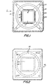
- a base 11 made of a high temperature thermoplastic material, such as a polyetherimide resin made by General Electric Co., Pittsfield, Mass., under the trade name Ultem.
- a recess 12 In the center of base 11 is a recess 12 in which an IC chip is eventually disposed.
- raised projections 12 Surrounding recess 12 are raised projections 14.
- Spaces 15 exist between the projections 14.
- On the inner end of each projection 14 is another raised portion 16.
- Raised portions 16 provided means for securing the leads in spaces 15 as shown in the above-described S.N. 584,080.
- slots 18 are formed by projections 29 which are similar to projections 14 but bigger.
- projections 29 are similar to projections 14 but bigger.
- raised portions 30 on the inner ends of projections 29, similar to raised portions 16 on projections 14.
- posts 22 on base 11 for accurate mating of base - 11 with cover 23, which is made of the same plastic as support 11.
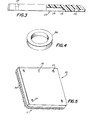
- Cover 23 (Figs. 2 and 3 ) has a recess 24 to mate with recess 12, and has an additional recess 25 to accommodate projections 14. Cover 23 also has a groove 26 rectangular in cross-section, to mate with trough 17, and four holes 27 into which posts 22 fit.
- a self-supporting, lead-in deformable sealant washer 36 (Fig.4) quadrangular in cross-section to match the configuration of groove 26 and trough 17, is provided within groove 26.
- Washer 36 is preferably formed from Amicon SE-617 or SE-628.
- Assembly of the components proceeds as follows.
- Four lead frame segments would be placed on top of base 11, one at a time and one in each quadrant, as shown in S.N.584,080.
- Each segment is carefully positioned so that the internal ends lay in spaces 15 and the external ends lay in slots 18.
- Pressure is then applied to the segments to ensure that they are flush against surface 13 and then, maintaining the pressure, heat is applied to portions 16 and 30 to cause them to flow over, and secure in place the internal ends and the external ends of the leads.
- This construction ensures accurate positioning, with secure attachment, of all of the leads with excellent co-planarity thereof.
- leads 4 can now be formed into a desired shape, such as "J" lead shape 34 showin in Fig. 5.
- Washer 36 is then placed in groove 26 of cover 23 and cover 23 is placed on support 11, posts 22 fitting into holes 27.
- Holes 27 are counterbored about half-way through as shown in Fig. 7, for example, to 43 mils diameter from 33 mile diameter.
- Posts 22 extend somewhat in the counterbores of holes 27, thereby providing the means for securing cover 23 to base 11 by heat-flowing the extending upper ends of posts 27, as raised portions 16 and 30 were heat-flowed.
- a lead identifier 32 may be used, as shown in Fig. 5.
Landscapes
- Structures Or Materials For Encapsulating Or Coating Semiconductor Devices Or Solid State Devices (AREA)
- Lead Frames For Integrated Circuits (AREA)
- Casings For Electric Apparatus (AREA)
- Die Bonding (AREA)
- Control And Other Processes For Unpacking Of Materials (AREA)
Applications Claiming Priority (2)
| Application Number | Priority Date | Filing Date | Title |
|---|---|---|---|
| US659212 | 1984-10-09 | ||
| US06/659,212 US4611398A (en) | 1984-10-09 | 1984-10-09 | Integrated circuit package |
Publications (2)
| Publication Number | Publication Date |
|---|---|
| EP0177948A2 true EP0177948A2 (fr) | 1986-04-16 |
| EP0177948A3 EP0177948A3 (fr) | 1988-01-20 |
Family
ID=24644521
Family Applications (1)
| Application Number | Title | Priority Date | Filing Date |
|---|---|---|---|
| EP85112798A Withdrawn EP0177948A3 (fr) | 1984-10-09 | 1985-10-09 | Boítier miniature pour circuit intégré |
Country Status (5)
| Country | Link |
|---|---|
| US (1) | US4611398A (fr) |
| EP (1) | EP0177948A3 (fr) |
| JP (1) | JPS6191950A (fr) |
| KR (1) | KR860003657A (fr) |
| CA (1) | CA1231182A (fr) |
Families Citing this family (6)
| Publication number | Priority date | Publication date | Assignee | Title |
|---|---|---|---|---|
| US5152057A (en) * | 1987-11-17 | 1992-10-06 | Mold-Pac Corporation | Molded integrated circuit package |
| US4868635A (en) * | 1988-01-13 | 1989-09-19 | Texas Instruments Incorporated | Lead frame for integrated circuit |
| US4829669A (en) * | 1988-04-28 | 1989-05-16 | Nec Corporation | Method of manufacturing a chip carrier |
| US5369059A (en) * | 1989-12-08 | 1994-11-29 | Cray Research, Inc. | Method for constructing a reduced capacitance chip carrier |
| US5780924A (en) * | 1996-05-07 | 1998-07-14 | Lsi Logic Corporation | Integrated circuit underfill reservoir |
| US5821607A (en) * | 1997-01-08 | 1998-10-13 | Orient Semiconductor Electronics, Ltd. | Frame for manufacturing encapsulated semiconductor devices |
Family Cites Families (9)
| Publication number | Priority date | Publication date | Assignee | Title |
|---|---|---|---|---|
| DE202925C (fr) * | 1969-04-30 | 1900-01-01 | ||
| US3265806A (en) * | 1965-04-05 | 1966-08-09 | Sprague Electric Co | Encapsulated flat package for electronic parts |
| US3684818A (en) * | 1970-10-20 | 1972-08-15 | Sprague Electric Co | Multi-layer beam-lead wiring for semiconductor packages |
| US3714370A (en) * | 1972-01-24 | 1973-01-30 | North American Rockwell | Plastic package assembly for electronic circuit and process for producing the package |
| US3981074A (en) * | 1974-08-23 | 1976-09-21 | Nitto Electric Industrial Co., Ltd. | Method for producing plastic base caps for split cavity type package semi-conductor units |
| US4139859A (en) * | 1975-06-30 | 1979-02-13 | Burroughs Corporation | Semiconductor device package |
| US4285002A (en) * | 1978-01-19 | 1981-08-18 | International Computers Limited | Integrated circuit package |
| GB2127740B (en) * | 1982-09-30 | 1985-10-23 | Burr Brown Res Corp | Improved hermetic sealing process |
| US4499333A (en) * | 1983-03-28 | 1985-02-12 | Printed Circuits International, Inc. | Electronic component cap and seal |
-
1984
- 1984-10-09 US US06/659,212 patent/US4611398A/en not_active Expired - Fee Related
-
1985
- 1985-08-01 KR KR1019850005546A patent/KR860003657A/ko not_active Withdrawn
- 1985-10-03 CA CA000492213A patent/CA1231182A/fr not_active Expired
- 1985-10-08 JP JP60222910A patent/JPS6191950A/ja active Pending
- 1985-10-09 EP EP85112798A patent/EP0177948A3/fr not_active Withdrawn
Also Published As
| Publication number | Publication date |
|---|---|
| CA1231182A (fr) | 1988-01-05 |
| JPS6191950A (ja) | 1986-05-10 |
| EP0177948A3 (fr) | 1988-01-20 |
| KR860003657A (ko) | 1986-05-28 |
| US4611398A (en) | 1986-09-16 |
Similar Documents
| Publication | Publication Date | Title |
|---|---|---|
| US4820658A (en) | Method of making a packaged IC chip | |
| US4653174A (en) | Method of making packaged IC chip | |
| US4870224A (en) | Integrated circuit package for surface mount technology | |
| US4957882A (en) | Method for manufacturing semiconductor device | |
| US3902148A (en) | Semiconductor lead structure and assembly and method for fabricating same | |
| EP0015111B1 (fr) | Cadre conducteur et boîtier pour circuit intégré | |
| US3413713A (en) | Plastic encapsulated transistor and method of making same | |
| US6175159B1 (en) | Semiconductor package | |
| CA1131724A (fr) | Condensateur et methode de fabrication | |
| US4554404A (en) | Support for lead frame for IC chip carrier | |
| JPS6143851B2 (fr) | ||
| US3444441A (en) | Semiconductor devices including lead and plastic housing structure suitable for automated process construction | |
| US4663650A (en) | Packaged integrated circuit chip | |
| US5152057A (en) | Molded integrated circuit package | |
| US4663651A (en) | Segmented lead frame strip for IC chip carrier | |
| US4611398A (en) | Integrated circuit package | |
| US4629824A (en) | IC package sealing technique | |
| US4215360A (en) | Power semiconductor device assembly having a lead frame with interlock members | |
| JPH08250641A (ja) | 半導体装置とその製造方法 | |
| EP0163856A1 (fr) | Procédé de fabrication d'un support de cadre d'interconnexions pour une puce à circuit intégré | |
| US5778520A (en) | Method of making an assembly package in an air tight cavity and a product made by the method | |
| US6011302A (en) | Semiconductor device with reduced amount of sealing resin | |
| EP0163082B1 (fr) | Puce à circuit intégré montée dans un boîtier | |
| EP0163081B1 (fr) | Procédé de fabrication d'une puce à circuit intégré encapsulée | |
| EP0163077B1 (fr) | Procédé de fabrication d'une puce à circuit intégré montée dans un boîtier |
Legal Events
| Date | Code | Title | Description |
|---|---|---|---|
| PUAI | Public reference made under article 153(3) epc to a published international application that has entered the european phase |
Free format text: ORIGINAL CODE: 0009012 |
|
| 17P | Request for examination filed |
Effective date: 19851009 |
|
| AK | Designated contracting states |
Kind code of ref document: A2 Designated state(s): AT BE DE FR GB IT NL |
|
| PUAL | Search report despatched |
Free format text: ORIGINAL CODE: 0009013 |
|
| AK | Designated contracting states |
Kind code of ref document: A3 Designated state(s): AT BE DE FR GB IT NL |
|
| 17Q | First examination report despatched |
Effective date: 19891106 |
|
| STAA | Information on the status of an ep patent application or granted ep patent |
Free format text: STATUS: THE APPLICATION IS DEEMED TO BE WITHDRAWN |
|
| 18D | Application deemed to be withdrawn |
Effective date: 19901005 |
|
| RIN1 | Information on inventor provided before grant (corrected) |
Inventor name: EAMES, ROBERT J. Inventor name: JOHNSON, RICHARD E. |