EP0178343B1 - Schaltnetzteil mit mehreren Ausgängen - Google Patents
Schaltnetzteil mit mehreren Ausgängen Download PDFInfo
- Publication number
- EP0178343B1 EP0178343B1 EP84112556A EP84112556A EP0178343B1 EP 0178343 B1 EP0178343 B1 EP 0178343B1 EP 84112556 A EP84112556 A EP 84112556A EP 84112556 A EP84112556 A EP 84112556A EP 0178343 B1 EP0178343 B1 EP 0178343B1
- Authority
- EP
- European Patent Office
- Prior art keywords
- output
- switching means
- current
- blanking pulses
- voltage
- Prior art date
- Legal status (The legal status is an assumption and is not a legal conclusion. Google has not performed a legal analysis and makes no representation as to the accuracy of the status listed.)
- Expired
Links
Images


Classifications
-
- H—ELECTRICITY
- H02—GENERATION; CONVERSION OR DISTRIBUTION OF ELECTRIC POWER
- H02M—APPARATUS FOR CONVERSION BETWEEN AC AND AC, BETWEEN AC AND DC, OR BETWEEN DC AND DC, AND FOR USE WITH MAINS OR SIMILAR POWER SUPPLY SYSTEMS; CONVERSION OF DC OR AC INPUT POWER INTO SURGE OUTPUT POWER; CONTROL OR REGULATION THEREOF
- H02M3/00—Conversion of DC power input into DC power output
- H02M3/22—Conversion of DC power input into DC power output with intermediate conversion into AC
- H02M3/24—Conversion of DC power input into DC power output with intermediate conversion into AC by static converters
- H02M3/28—Conversion of DC power input into DC power output with intermediate conversion into AC by static converters using discharge tubes with control electrode or semiconductor devices with control electrode to produce the intermediate AC
- H02M3/325—Conversion of DC power input into DC power output with intermediate conversion into AC by static converters using discharge tubes with control electrode or semiconductor devices with control electrode to produce the intermediate AC using devices of a triode or a transistor type requiring continuous application of a control signal
- H02M3/335—Conversion of DC power input into DC power output with intermediate conversion into AC by static converters using discharge tubes with control electrode or semiconductor devices with control electrode to produce the intermediate AC using devices of a triode or a transistor type requiring continuous application of a control signal using semiconductor devices only
- H02M3/33561—Conversion of DC power input into DC power output with intermediate conversion into AC by static converters using discharge tubes with control electrode or semiconductor devices with control electrode to produce the intermediate AC using devices of a triode or a transistor type requiring continuous application of a control signal using semiconductor devices only having more than one ouput with independent control
Definitions
- This invention relates to an improved multiple output switching power supply that provides a number of different regulated output voltages at the outputs of a number of secondary windings of a power transformer.
- a main output direct current voltage is derived from one secondary winding and regulated by modulating the width of pulses of current flowing in the primary winding of the transformer.
- Auxiliary direct current output voltages are derived by rectifying the voltage at each of the other secondary windings and each is controlled by its own regulator.
- a storage filter is required between the secondary winding and the control transistor.
- Compactness is usually attained by using high switching frequencies for the pulse width modulation process so as to reduce the size of transformer and filters.
- the switching frequency is limited by the performances of the transistors and by the trade off of the efficiency decrease, due to switching power losses in the transistors.
- US Pat. 4,122,514 discloses a D.C. power supply where auxiliary output voltages are controlled by SCR devices triggered by a control circuit response to the ripple of the auxiliary output voltage.
- a pulse width modulation of the pulsed power feeding the auxiliary output is obtained which overlap the pulsed power feeding of the transformer, controlled by the main output voltage regulator.
- SCR Limiting the operating switching frequency of the power supply as compared to the switching frequency allowed by faster devices such as transistors and more recently power FETs (Field effect transistors).
- the SCRs and the primary winding switches are fully affected by the current spikes caused by the free-wheel diode associated to each output filter when such SCR are switched on.
- the switching transistors controlling the current flowing in the primary winding of the transformer must switch-off the full equivalent current feeding both the main output section and all the auxiliary output sections.
- the direct current power supply of the present invention overcomes such disadvantages and provides for a power system having at least an auxiliary output voltage, where no auxiliary intermediate filter is required, and where switch-off losses of switching transistors are minimized.
- a common oscillator establishes the switching frequency for both the main output control circuit and the auxiliary output(s) control circuit(s).
- the common oscillator provides a clock signal which triggers a first pulse width modulation circuit which control switching on/off of the main output control transistors, and second(s) pulse width modulation circuit(s) which control switching off of auxiliary output(s) control transistors within the period during which the main output control transistors are conductive.
- Figure 1 shows a power supply implemented as disclosed by U.S. Pat. 4,122,154.
- a D.C. source, 101 feeds the primary winding 102 of a transformer T, through a pair of capacitors 103, 104 series connected across the DC power source, and a pair of transistors, 105, 106, alternatively driven in conduction by a base drive circuit 107, controlled by an oscillator 108 and a pulse width modulation circuit 109.
- the pulse width modulation circuit is responsive to the voltage sensed at a main output V1 of the power supply, which is fed, through a LC filter (comprising capacitor 110 and inductor 111) and a pair of diodes 112, 113, by a center tapped secondary winding 114 of the transformer T.
- Oscillator 108 defines the period at which transistors 105, 106 are alternatively switched-on and pulse width modulation circuit defines the variable interval duration which transistors 105, 106 are kept conductive.
- Such duration is inversely proportional to the error of detected voltage V1 in excess over a preestablished reference value.
- Figure 2 shows in timing diagram (A) the current flowing in the primary winding 102, which is required to maintain the desired voltage at output V1.
- the time interval P between subsequent alternate current pulses is defined by oscillator 108.
- the pulse width W is defined by modulator 109, within period P and varies in dependence of the detected voltage V1, which in turn is affected by the power drained by a load 15.
- a further secondary, center tapped auxiliary winding 16 is provided, which feeds a LC filter (composed of inductor 17 and capacitor 18) through a pair of controlling SCRs 19, 20, alternatively triggered by a base drive circuit 21.
- the base drive circuit 21 is controlled by a comparator 22, responsive to the voltage V2 at capacitor 18 terminals.
- Either SCR19 or SCR20 remain conductive until voltage is induced in winding 16 due to the feeding of primary winding 102.
- a free wheel diode 23 is coupled to inductor 17 and capacitor 18 to sustain current in inductor 17 when either SCR 19 or 20 switch-off.
- Figure 2 shows in timing diagram B the equivalent current flowing in the primary winding 102 owing to the operation of auxiliary output circuit fed by auxiliary winding 16.
- SCR 19 or 20 is triggered to switch-on when voltage is already induced in winding 16, at an instant depending on comparator 22 detecting a voltage V2 drop below the reference value.
- free wheel diode 23 is forward biased in conduction, and, if a sudden reverse voltage is applied, it acts as a short circuit, until the junction charge is removed, then as a capacitor, until a reverse bias charge is built up.
- Figure 2 shows in diagram C the current flowing in the primary winding owing to the combined operation of the main output and auxiliary output.
- Transistors 105, 106 are affected by turn on losses, proportional to the equivalent current amplitude of the pulses in the secondary winding 114.
- the SCR are affected by turn-on losses, which exceed the average current amplitude of the pulses at secondary winding 16, due to the initial current spike.
- Transistors 105, 106 must be current rated in order to sustain the sum of the equivalent current amplitude of pulses in secondary winding 114, the equivalent current amplitude of pulses in secondary winding 16 and the current spikes amplitude due to freewheel diode 23.
- SCR 19, 20 must be current rated in order to sustain the sum of the average current amplitude of pulses in secondary winding 16 and the current amplitude due to freewheel diode 23.
- Transistors 105, 106 are switched-off at a substantially full current load, and cause transformer ringing at high frequency, with high current levels.
- SCR SCR as switches
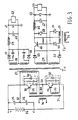
- Figure 3 shows the power section of a multiple output power supply designed according to the invention, which overcomes the above mentioned limitation.
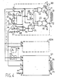
- Figure 4 shows the control section of the power supply of Figure 3.
- the power supply of the invention comprises an unregulated DC power source 24 (which may be obtained from a rectified DC source) a pair of capacitors 25, 26 series connected to the terminals of the DC power source, a transformer TO having a primary winding 27 and two center tapped, secondary windings 28, 29.
- a pair of transistors 30, 31, series connected between the terminals of the DC power source 24 control the alternate current flowing in primary winding 27 which is connected to the intermediate point 32 between capacitors 25, 26 and the intermediate point 33 between transistors 30, 31 (through regenerative winding 80).
- Transistors 30, 31 are transformer driven, through transformer T1, having a primary winding 34, regenerative winding 80 and two secondary windings 35, 36, each coupled to the base and emitter of transistors 30, 31 respectively.
- a snubber element 81, 82 comprised of a bypass diode, and an RC path is coupled between collector and emitter of transistors 30, 31.
- the transistors 30, 31, are alternatively switched on and current pulses of alternated polarity are let to flow in primary winding 27.
- Terminals of center tapped secondary winding 28 are coupled through diodes 37, 38 to an input terminal of an LC filter comprised of inductor 39 and capacitor 40.
- the other input terminal of LC filter is connected to the center tap of winding 28, which is also grounded.
- Voltage V1 feeds a load 42 and, as shown in Figure 4, provides a feedback signal to the control circuit.
- Terminals of center tapped secondary winding 29 are coupled, through diodes 43, 44 to the collector of a control transistor switch 45. Center tap is grounded.
- Emitter of transistor 45 is connected to input of an LC filter comprised of inductor 46, capacitor 47 and freewheel diode 48.
- Transistor 45 is controlled by current pulses applied to its base through a transformer T2 having a center tapped secondary winding 49 whose terminal are connected, through diodes 50, 51 to the transistor base, the center tap being connected to the emitter.
- Suitable circuits exemplified by resistor 83, provide transistor turn off at termination of current pulses.
- Voltage V2 feeds a load 53 and, as shown in Figure 4 provides a feedback signal to the control circuit.
- an error signal is developed which is used to control the width of the pulses which switch on transistor 45, thus modulating the power fed to LC filter 46, 47 and keeping V2 close to the desired value.
- the power supply is shown as having two secondary outputs only, but clearly more than two outputs may be provided.
- Figure 4 shows the control section of the power supply of the present invention, which is essentially comprised of a plurality of regulating pulse width modulators 60, 61, 60N one for each secondary output, and suitably connected each other.
- Such regulating pulse width modulators are available on the market as integrated circuits, such as for instance those marketed by the US firm Unitrode, with code UC 3525A.
- Regulating pulse width modulator 60 comprises a sawtooth oscillator 62, a toggle flip-flop 63, two NOR circuits 64, 65 having both inverting and non inverting output, four output transistors 85, 66, 67, 68, an error amplifier 69, a comparator 70 and a Set-Reset flip-flop 71.
- the oscillator 62 frequency is determined by three external components, a resistor 72 connected between ground and pin 6 of the integrated circuit, a capacitor 73 connected between ground and pin 5 of the circuit and a resistor 74 connected between pins 5 and 7 of the circuit.
- Value of resistor 72 defines the current level provided by a constant current generator (internal to oscillator 62) to capacitor 73.
- value of resistor 72 and value of capacitor 73 jointly define the interval time required for charging capacitor 73 to a preestablished voltage level.
- oscillator 62 delivers, internally to circuit 60 and to pin 4 a positive blanking pulse which also enables capacitor 73 to discharge through resistor 74.
- the interval time required to discharge capacitor 73 at another preestablished level is defined by value of resistor 74. Once capacitor 73 is discharged, the positive blanking pulse available at pin 4 drops to zero.
- the sum of charge and discharge time of capacitor 73 defines the oscillator period (hence frequency).
- the sawtooth voltage signal, available at pin 5 and the blanking pulses available at pin 4 are used to control the other circuit elements.
- Error amplifier 69 receives at non inverting input (Pin 2) a reference voltage VREF2 and at inverting input (Pin 1) the voltage V2 sensed at the auxiliary output 52 ( Figure 3).
- Error amplifier 69 produce at the output a positive error voltage signal, whose amplitude is the more greater the more voltage V2 is below the reference signal.
- the error voltage signal is fed to the inverting input of comparator 70 which receives at the non inverting input the sawtooth voltage signal available on pin 5.
- the positive blanking pulses generated by oscillator 62 and available at pin 4 provide the reset of flip-flop 71.
- NOR gate 65 receives at its input the signal in output from flip-flop 71, the signal in output from Q output of flip-flop 63 and the blanking pulses in output from oscillator 62.
- the inverting and non inverting outputs of NOR gate 64 respectively drive transistors 66, 67 in totem pole connection, to connect, through pin 11 a terminal of winding 75 to a voltage source +V or to ground.
- the inverting and non inverting outputs of NOR gate 65 respectively drive transistor 68, 85 in totem pole connection, to connect through pin 14 the other terminal of winding 75 to the voltage source +V or to ground.
- Winding 75 is the primary winding of transformer T2 ( Figure 3).
- Energization voltage +V is applied to winding 75 in alternate direction at each subsequent period of the oscillator, during the interval in which capacitor 73 charges, and until a charge level is attained which exceeds the error signal. Thereafter energization is interrupted.
- the width of such energization interval depends on the error signal and may range from zero to the full duration of the capacitor charge time.
- blanking pulses prevents any energization of winding 75.
- Pulse width modulator 61 has pins 11, 14 connected to primary winding 34 of transformer T1 and controls main output voltage V1, which is fed back to input pin 1 and compared with a reference voltage VREF1 applied to input pin 2.
- regulators 60, 61, 60N are synchronized in order to achieve the desired results, which are, besides the avoidance of intermediate storage filters between auxiliary windings such as 29, and related control switch, such as 45, the minimization of switching power losses, current spikes and radio frequency emission.
- Control of their internal flip-flops (corresponding to flip-flops 63, 71) and output gates (corresponding to NOR 64, 65) is performed by directly connecting pin 4 of regulator 60 with corresponding pin 4 of possible regulator 60N and by connecting pin 4 or regulator 60 with corresponding pin 4 of regulator 61 through a delay element 77, for instance in the form of series connected inverters or logic gates. Therefore blanking pulses are fed, without or with delay from regulator 60 to regulators 60N, 61.
- regulator 60N which lead generation and distribution of blanking pulses to the other regulators, the duration of blanking pulses being always imposed by the discharge time of capacitor 73 hence by oscillator 62.
- pin 4 of regulator 60 is connected to synchronization pin 3 of-regulator 61.
- Diagram A shows the voltage saw tooth signal available at pin 5 of each and all regulators 60, 60N, 61, as well as an exemplary level of errors signals E2, E1.
- Diagram B shows the blanking pulses available at pin 4 of regulators 60, 60N.
- Diagram C shows the blanking pulses available at pin 4 of regulator 61.
- Diagram D shows the voltage pulses applied to winding 75.
- Such pulses have a variable width, raising with the falling edge of blanking pulses in B and dropping when the sawtooth signal exceed the error voltage E2.
- Diagram E shows the voltage pulses applied to winding 34.
- Such pulses have a variable width, raising with the falling edge of blanking pulses in C and dropping when the sawtooth signal exceeds the error voltage E1.
- Voltage pulses shown in diagrams D, E controls the turn-on, turn-off of transistor 45 and transistors 30, 31, respectively.
- transistor 45 is turned-on and turned-off in advance of transistor 30, 31.
- transistors 30, 31 when transistors 30, 31 are turned-off, they switch-off the current-equivalent flowing in winding 28 and feeding inductor 39 and main load 42, not the current equivalent flowing in winding 29.
- the transformer ringing is limited in amplitude due to the fact that switched off current is the only equivalent current of secondary winding 28.
- transistor 45 When transistor 45 is switched-on no e.m. force is induced in winding 29, therefore no substantial voltage is applied between collector and emitter of transistor 45 which is brought to saturation substantially without switching losses.
- the voltage and current rise in the secondary winding is not abrupt but smoothed, due to several factors:
- the slow voltage raising in windings 28, 29 allows for the reverse biasing of diode 48, and the relevant diode in the pairs 37, 38 and 43, 44 (depending on the direction of the induced e.m. force) substantially without current peaks due to diode reverse biasing currents.
- switch-on losses in transistors 30, 31 are minimized because turn-on occurs at low current level and is not affected or remarkably affected by overshooting.
- transistors 30, 31 may be selected, having a lower current rating then required to withstand unpredictable level current spikes and higher reliability is achieved.
- Diagram F in Fig. 5 shows the equivalent current flowing in the primary winding of transformer T0.
- delay element 77 shows that substantial advantages are achieved thanks to delay element 77 or by adopting an operation concept for the power supply which may be defined switch-on synchronization among regulating sections, with delay of the main regulating section, controlled at primary winding as to auxiliaries sections, controlled at secondary windings.
- power MOS field effect transistors may be used for controlling current of the auxiliary windings, together with bipolar transistors controlling the main windings.
- MOS FET have a switching time which is typically in the range of 100 to 200 nsec. against a turn-off/turn-on time of power switching bipolar transistor which is in the range of 400 to 600 nsec., not to consider the delay caused by the driving circuit.
- switches such as 45 of Fig. 3 when implemented by MOS FET, may become full conductive well before switches such as 30, 31, implemented by bipolar transistors become full conductive even if both switches are driven in perfect synchronization by the same pulse.
- driving of such switches through driving transformers is only exemplary and different form of coupling, such as direct coupling, can be used.
- regulating pulse width modulator 60 performs both the function of master oscillator, for generation of periodical blanking pulses, and sawtooth signal generator
- an independent master oscillator triggers a plurality of independent saw tooth signal generators and a plurality of pulse width modulators each responsive to a different and independent saw tooth signal.
Landscapes
- Engineering & Computer Science (AREA)
- Power Engineering (AREA)
- Dc-Dc Converters (AREA)
Claims (3)
Priority Applications (3)
| Application Number | Priority Date | Filing Date | Title |
|---|---|---|---|
| EP84112556A EP0178343B1 (de) | 1984-10-18 | 1984-10-18 | Schaltnetzteil mit mehreren Ausgängen |
| DE8484112556T DE3476307D1 (en) | 1984-10-18 | 1984-10-18 | Multiple output switching power supply |
| US06/775,863 US4646217A (en) | 1984-10-18 | 1985-09-13 | Multiple outputs switching power supply |
Applications Claiming Priority (1)
| Application Number | Priority Date | Filing Date | Title |
|---|---|---|---|
| EP84112556A EP0178343B1 (de) | 1984-10-18 | 1984-10-18 | Schaltnetzteil mit mehreren Ausgängen |
Publications (2)
| Publication Number | Publication Date |
|---|---|
| EP0178343A1 EP0178343A1 (de) | 1986-04-23 |
| EP0178343B1 true EP0178343B1 (de) | 1989-01-18 |
Family
ID=8192226
Family Applications (1)
| Application Number | Title | Priority Date | Filing Date |
|---|---|---|---|
| EP84112556A Expired EP0178343B1 (de) | 1984-10-18 | 1984-10-18 | Schaltnetzteil mit mehreren Ausgängen |
Country Status (3)
| Country | Link |
|---|---|
| US (1) | US4646217A (de) |
| EP (1) | EP0178343B1 (de) |
| DE (1) | DE3476307D1 (de) |
Families Citing this family (18)
| Publication number | Priority date | Publication date | Assignee | Title |
|---|---|---|---|---|
| US4833582A (en) * | 1987-03-27 | 1989-05-23 | Siemens Aktiengesellschaft | Frequency converter circuit including a single-ended blocking frequency converter |
| DE3805460A1 (de) * | 1988-02-22 | 1989-08-31 | Kabelmetal Electro Gmbh | Verfahren zum betreiben eines elektrischen stromversorgungsgeraets mit gleichspannungswandler |
| US4945465A (en) * | 1988-09-15 | 1990-07-31 | U.S. Philips Corporation | Switched-mode power supply circuit |
| IT1231052B (it) * | 1989-09-27 | 1991-11-12 | Bull Hn Information Syst | Alimentatore a commutazione con piu' uscite, regolazione di una tensione di uscita e compensazione di carico. |
| JPH04183275A (ja) * | 1990-11-16 | 1992-06-30 | Honda Motor Co Ltd | パルス幅変調制御装置 |
| CA2124370C (en) * | 1994-05-26 | 1998-09-29 | Ivan Meszlenyi | Self oscillating dc to dc converter |
| ES2101640B1 (es) * | 1994-10-24 | 1997-12-16 | Telefonica Nacional Espana Co | Circuito convertidor de alimentacion. |
| JP3563816B2 (ja) * | 1995-03-08 | 2004-09-08 | キヤノン株式会社 | スイッチング電源装置 |
| ES2107949B1 (es) * | 1995-03-17 | 1998-07-01 | Telefonica Nacional Espana Co | Circuito convertidor de alimentacion. |
| JP2900876B2 (ja) * | 1996-03-19 | 1999-06-02 | サンケン電気株式会社 | 表示装置の電源装置 |
| US5907481A (en) * | 1997-10-31 | 1999-05-25 | Telefonaktiebolaget Lm Ericsson | Double ended isolated D.C.--D.C. converter |
| US6359795B1 (en) * | 1999-03-26 | 2002-03-19 | Sarnoff Corporation | Soft-switching power supply with auxiliary resonator |
| CN1771655A (zh) * | 2002-12-31 | 2006-05-10 | 阿波吉技术公司 | 自适应性谐振开关电源系统 |
| US8737099B2 (en) * | 2011-07-15 | 2014-05-27 | O2Micro, Inc. | Controllers for power converters |
| US9397579B2 (en) | 2011-07-15 | 2016-07-19 | O2Micro Inc | Full-bridge switching DC/DC converters and controllers thereof |
| EP3219004B1 (de) * | 2014-11-10 | 2021-02-17 | Esab Ab | Schweissvorrichtung mit mehreren spannungen |
| WO2017223038A1 (en) * | 2016-06-20 | 2017-12-28 | Ionel Jitaru | Very high efficiency soft switching converter aka the adjud converter |
| US10554134B2 (en) * | 2017-06-02 | 2020-02-04 | Power Integrations, Inc. | Idle ring detection for a multi-output power converter |
Family Cites Families (2)
| Publication number | Priority date | Publication date | Assignee | Title |
|---|---|---|---|---|
| US4122514A (en) * | 1976-11-01 | 1978-10-24 | Hewlett-Packard Company | Direct current power supply |
| JPS54140154A (en) * | 1978-04-24 | 1979-10-31 | Toshiba Corp | Stabilized dc power source equipment |
-
1984
- 1984-10-18 EP EP84112556A patent/EP0178343B1/de not_active Expired
- 1984-10-18 DE DE8484112556T patent/DE3476307D1/de not_active Expired
-
1985
- 1985-09-13 US US06/775,863 patent/US4646217A/en not_active Expired - Fee Related
Also Published As
| Publication number | Publication date |
|---|---|
| DE3476307D1 (en) | 1989-02-23 |
| US4646217A (en) | 1987-02-24 |
| EP0178343A1 (de) | 1986-04-23 |
Similar Documents
| Publication | Publication Date | Title |
|---|---|---|
| US4646217A (en) | Multiple outputs switching power supply | |
| US5875103A (en) | Full range soft-switching DC-DC converter | |
| US4706177A (en) | DC-AC inverter with overload driving capability | |
| US5781419A (en) | Soft switching DC-to-DC converter with coupled inductors | |
| US4323961A (en) | Free-running flyback DC power supply | |
| US4365171A (en) | Low loss snubber circuit | |
| EP1356575B1 (de) | Isolierte treiberschaltungsanordnung zur verwendung in leistungsschaltreglern | |
| US5886884A (en) | Passive ripple filter for zero voltage-zero current switched full-bridge DC/DC converters | |
| EP0389154B1 (de) | Selbstschwingender Wandler mit Leichtlast-Stabilisator | |
| US4623960A (en) | Bias power source energized by tertiary winding including hysteresis characteristic for disabling the power switch when a minimum base drive signal can no longer be maintained | |
| US4007413A (en) | Converter utilizing leakage inductance to control energy flow and improve signal waveforms | |
| EP0385546B1 (de) | Geschaltete Speisespannungsschaltung mit Anlaufschaltung | |
| JPH0832162B2 (ja) | 直流−直流変換器及び直流−直流変換方法 | |
| US4312029A (en) | DC-to-DC Converter with reduced power loss during turn off | |
| US20020118503A1 (en) | Gate driver for thyristor | |
| EP0079130B1 (de) | Verlustfreier Ausschalt-Entlastungskreis für mit Klemmdioden beschaltete Induktivlast | |
| EP0124210A1 (de) | Energieversorgung mit stromgesteuertem Sperrwandler | |
| US4499530A (en) | Switching power supply apparatus | |
| US4864485A (en) | Switched mode power supply with start-up control | |
| JPH10262380A (ja) | 電流給電装置 | |
| US6661209B2 (en) | Leading edge modulator for post regulation of multiple output voltage power supplies | |
| US5841642A (en) | Tuned switch-mode power supply with current mode control | |
| US3293532A (en) | Switching and flyback techniques in regulated d. c. power supplies | |
| US5229930A (en) | Welding inverter and method for controlling a welding inverter | |
| EP0030829B1 (de) | Sperrwandler |
Legal Events
| Date | Code | Title | Description |
|---|---|---|---|
| PUAI | Public reference made under article 153(3) epc to a published international application that has entered the european phase |
Free format text: ORIGINAL CODE: 0009012 |
|
| 17P | Request for examination filed |
Effective date: 19851008 |
|
| AK | Designated contracting states |
Kind code of ref document: A1 Designated state(s): DE FR GB IT |
|
| 17Q | First examination report despatched |
Effective date: 19870625 |
|
| RAP1 | Party data changed (applicant data changed or rights of an application transferred) |
Owner name: HONEYWELL BULL ITALIA S.P.A. |
|
| GRAA | (expected) grant |
Free format text: ORIGINAL CODE: 0009210 |
|
| ITF | It: translation for a ep patent filed | ||
| AK | Designated contracting states |
Kind code of ref document: B1 Designated state(s): DE FR GB IT |
|
| REF | Corresponds to: |
Ref document number: 3476307 Country of ref document: DE Date of ref document: 19890223 |
|
| ET | Fr: translation filed | ||
| PLBE | No opposition filed within time limit |
Free format text: ORIGINAL CODE: 0009261 |
|
| STAA | Information on the status of an ep patent application or granted ep patent |
Free format text: STATUS: NO OPPOSITION FILED WITHIN TIME LIMIT |
|
| 26N | No opposition filed | ||
| PGFP | Annual fee paid to national office [announced via postgrant information from national office to epo] |
Ref country code: GB Payment date: 19921007 Year of fee payment: 9 |
|
| PGFP | Annual fee paid to national office [announced via postgrant information from national office to epo] |
Ref country code: FR Payment date: 19921027 Year of fee payment: 9 |
|
| ITTA | It: last paid annual fee | ||
| PG25 | Lapsed in a contracting state [announced via postgrant information from national office to epo] |
Ref country code: GB Effective date: 19931018 |
|
| PGFP | Annual fee paid to national office [announced via postgrant information from national office to epo] |
Ref country code: DE Payment date: 19931021 Year of fee payment: 10 |
|
| GBPC | Gb: european patent ceased through non-payment of renewal fee |
Effective date: 19931018 |
|
| PG25 | Lapsed in a contracting state [announced via postgrant information from national office to epo] |
Ref country code: FR Effective date: 19940630 |
|
| REG | Reference to a national code |
Ref country code: FR Ref legal event code: ST |
|
| PG25 | Lapsed in a contracting state [announced via postgrant information from national office to epo] |
Ref country code: DE Effective date: 19950701 |