EP0178662A2 - Verfahren zur Herstellung eines Halbleiterbeschleunigungsmessers - Google Patents
Verfahren zur Herstellung eines Halbleiterbeschleunigungsmessers Download PDFInfo
- Publication number
- EP0178662A2 EP0178662A2 EP85113191A EP85113191A EP0178662A2 EP 0178662 A2 EP0178662 A2 EP 0178662A2 EP 85113191 A EP85113191 A EP 85113191A EP 85113191 A EP85113191 A EP 85113191A EP 0178662 A2 EP0178662 A2 EP 0178662A2
- Authority
- EP
- European Patent Office
- Prior art keywords
- etching
- substrate
- cantilevered
- weight
- type
- Prior art date
- Legal status (The legal status is an assumption and is not a legal conclusion. Google has not performed a legal analysis and makes no representation as to the accuracy of the status listed.)
- Granted
Links
Images


Classifications
-
- G—PHYSICS
- G01—MEASURING; TESTING
- G01P—MEASURING LINEAR OR ANGULAR SPEED, ACCELERATION, DECELERATION, OR SHOCK; INDICATING PRESENCE, ABSENCE, OR DIRECTION, OF MOVEMENT
- G01P15/00—Measuring acceleration; Measuring deceleration; Measuring shock, i.e. sudden change of acceleration
- G01P15/02—Measuring acceleration; Measuring deceleration; Measuring shock, i.e. sudden change of acceleration by making use of inertia forces using solid seismic masses
- G01P15/08—Measuring acceleration; Measuring deceleration; Measuring shock, i.e. sudden change of acceleration by making use of inertia forces using solid seismic masses with conversion into electric or magnetic values
- G01P15/12—Measuring acceleration; Measuring deceleration; Measuring shock, i.e. sudden change of acceleration by making use of inertia forces using solid seismic masses with conversion into electric or magnetic values by alteration of electrical resistance
- G01P15/123—Measuring acceleration; Measuring deceleration; Measuring shock, i.e. sudden change of acceleration by making use of inertia forces using solid seismic masses with conversion into electric or magnetic values by alteration of electrical resistance by piezo-resistive elements, e.g. semiconductor strain gauges
-
- F—MECHANICAL ENGINEERING; LIGHTING; HEATING; WEAPONS; BLASTING
- F16—ENGINEERING ELEMENTS AND UNITS; GENERAL MEASURES FOR PRODUCING AND MAINTAINING EFFECTIVE FUNCTIONING OF MACHINES OR INSTALLATIONS; THERMAL INSULATION IN GENERAL
- F16C—SHAFTS; FLEXIBLE SHAFTS; ELEMENTS OR CRANKSHAFT MECHANISMS; ROTARY BODIES OTHER THAN GEARING ELEMENTS; BEARINGS
- F16C11/00—Pivots; Pivotal connections
- F16C11/04—Pivotal connections
- F16C11/12—Pivotal connections incorporating flexible connections, e.g. leaf springs
-
- G—PHYSICS
- G01—MEASURING; TESTING
- G01P—MEASURING LINEAR OR ANGULAR SPEED, ACCELERATION, DECELERATION, OR SHOCK; INDICATING PRESENCE, ABSENCE, OR DIRECTION, OF MOVEMENT
- G01P15/00—Measuring acceleration; Measuring deceleration; Measuring shock, i.e. sudden change of acceleration
- G01P15/02—Measuring acceleration; Measuring deceleration; Measuring shock, i.e. sudden change of acceleration by making use of inertia forces using solid seismic masses
- G01P15/08—Measuring acceleration; Measuring deceleration; Measuring shock, i.e. sudden change of acceleration by making use of inertia forces using solid seismic masses with conversion into electric or magnetic values
- G01P15/0802—Details
-
- G—PHYSICS
- G01—MEASURING; TESTING
- G01P—MEASURING LINEAR OR ANGULAR SPEED, ACCELERATION, DECELERATION, OR SHOCK; INDICATING PRESENCE, ABSENCE, OR DIRECTION, OF MOVEMENT
- G01P15/00—Measuring acceleration; Measuring deceleration; Measuring shock, i.e. sudden change of acceleration
- G01P15/02—Measuring acceleration; Measuring deceleration; Measuring shock, i.e. sudden change of acceleration by making use of inertia forces using solid seismic masses
- G01P15/08—Measuring acceleration; Measuring deceleration; Measuring shock, i.e. sudden change of acceleration by making use of inertia forces using solid seismic masses with conversion into electric or magnetic values
- G01P15/125—Measuring acceleration; Measuring deceleration; Measuring shock, i.e. sudden change of acceleration by making use of inertia forces using solid seismic masses with conversion into electric or magnetic values by capacitive pick-up
-
- H—ELECTRICITY
- H10—SEMICONDUCTOR DEVICES; ELECTRIC SOLID-STATE DEVICES NOT OTHERWISE PROVIDED FOR
- H10P—GENERIC PROCESSES OR APPARATUS FOR THE MANUFACTURE OR TREATMENT OF DEVICES COVERED BY CLASS H10
- H10P50/00—Etching of wafers, substrates or parts of devices
- H10P50/60—Wet etching
- H10P50/61—Electrolytic etching
- H10P50/613—Electrolytic etching of Group IV materials
-
- G—PHYSICS
- G01—MEASURING; TESTING
- G01P—MEASURING LINEAR OR ANGULAR SPEED, ACCELERATION, DECELERATION, OR SHOCK; INDICATING PRESENCE, ABSENCE, OR DIRECTION, OF MOVEMENT
- G01P15/00—Measuring acceleration; Measuring deceleration; Measuring shock, i.e. sudden change of acceleration
- G01P15/02—Measuring acceleration; Measuring deceleration; Measuring shock, i.e. sudden change of acceleration by making use of inertia forces using solid seismic masses
- G01P15/08—Measuring acceleration; Measuring deceleration; Measuring shock, i.e. sudden change of acceleration by making use of inertia forces using solid seismic masses with conversion into electric or magnetic values
- G01P2015/0805—Measuring acceleration; Measuring deceleration; Measuring shock, i.e. sudden change of acceleration by making use of inertia forces using solid seismic masses with conversion into electric or magnetic values being provided with a particular type of spring-mass-system for defining the displacement of a seismic mass due to an external acceleration
- G01P2015/0822—Measuring acceleration; Measuring deceleration; Measuring shock, i.e. sudden change of acceleration by making use of inertia forces using solid seismic masses with conversion into electric or magnetic values being provided with a particular type of spring-mass-system for defining the displacement of a seismic mass due to an external acceleration for defining out-of-plane movement of the mass
- G01P2015/0825—Measuring acceleration; Measuring deceleration; Measuring shock, i.e. sudden change of acceleration by making use of inertia forces using solid seismic masses with conversion into electric or magnetic values being provided with a particular type of spring-mass-system for defining the displacement of a seismic mass due to an external acceleration for defining out-of-plane movement of the mass for one single degree of freedom of movement of the mass
- G01P2015/0828—Measuring acceleration; Measuring deceleration; Measuring shock, i.e. sudden change of acceleration by making use of inertia forces using solid seismic masses with conversion into electric or magnetic values being provided with a particular type of spring-mass-system for defining the displacement of a seismic mass due to an external acceleration for defining out-of-plane movement of the mass for one single degree of freedom of movement of the mass the mass being of the paddle type being suspended at one of its longitudinal ends
Definitions
- micro-miniature accelerometer which is formed on a semiconductor substrate.
- Another object of the invention is to provide a method of manufacturing for semiconductor accelerometer without a strict controlling on the temperature of an etching solution and the duration for etching.
- the present invention is arrnaged to form the portion which is to becomes the cantilevered Si beam (including the Si weight) as a second conduction type (n-type, for instance), encompass its rim with a first conduction type (p-type, for instance), and by etching the portion of the first conducton type alone with the electrochemical etching that does not proceed beyond the p-n junction section, to form the support section of the cantilevered beam, that is of semiconductor of the first conduction type, with semiconductor of the second conduction type.
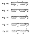
- Fig. 2(A) in the first step, following the formation of a diffused resistor which is not shown on the n-type Si substrate 21, both of the top and bottom surfaces are coated with thermal oxide films tSi0 2 ).
- 22 is the top surface thermal oxide film while 23 is the bottom surface thermal oxide film.
- the cavity 26 for the upper air gap is formed by photoetching on the top surface thermal oxide film 22.
- This etching is continued until there is formed an air gap 28.
- both of the top surface thermal oxide film 22 and the bottom surface thermal oxide film 23 are removed.
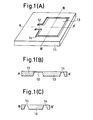
- Figs. 3(A) through 3(F) are shown a perspective view and a cross section view of an embodiment of the semiconductor accelerometer manufactured in accordance with the present invention, in which Figs. 3(A) through 3(C) illustrate the structure before etching, that is, before the formation of a cantilevered Si beam while Figs. 3(D) through 3(F) illustrate the structure after etching, that is, after the formation of the cantilevered Si beam.
- an n-type Si layer 32 is formed on a p-type Si substrate 31.
- the thickness of the Si layer 32 is set to be identical to the thickness of the cantilevered Si beam.
- the Si region 33 is formed from the surface of the Si layer 12 to the deptch until it reaches the Si substrate 31.
- the p-type portions namely, the Si substrate 31 and the Si region 33, are removed in one operation by the Si etching with the mask that is provided on the back surface of the substrate 31.
- FIGs. 4(A) through 4(G) is shown the manufacturing process according to the present invention.
- an epitaxial layer is more general, but an n-type impurity diffused layer will do also.
- a thermal oxide film SiO 2
- PSG phospho-silicate glass
- the Si region 44 which is the portion that is to become the air gap that determines the external form of the cantilevered beam and the weight, has to be diffused deep from'the surface of the Si layer 42 until it reaches the Si substrate 41.
- a part of the upper insulating film 43 is removed in order to form a contact section 45 for applying voltage to the Si layer 42 in carrying out the electrochemical etching.
- a metallic (aluminum or others) film is formed on the entire top surface to create an electrode 46.
- portions, namely, the opening section 48 for the cantilevered beam and the drilling section 49 for the air gap, of the lower insulating film that is formed on the back surface of the Si substrate 41 are removed by photoetching to form a mask for the back surface etching.
- the n-type Si layer 42 alone is protected by the voltage to increase the resistivity to the etching so that the etching proceeds only in the areas of the p-type Si substrate 41 and Si region 44, until it is halted at the p-n junction surface which is the boundary between 41, 44 and 42.
- the upper insulating film 43 which is above the air gap 52 is removed by carrying out an etching from the back surface.
- a Si wafer 53 and a cathode 55 (Pt or other metal is used in general) are immersed in a Si etching solution 54 in an etching bath 57.
- a voltage of order of 0.6V from the power supply 56 is applied between the electrode 46 on the surface of the Si wafer 53 and the cathode 55.
- the positive voltage which is given by the power supply 56 through the electrode 46 is applied only to the n-type Si layer 42 so that the Si layer 42 alone is protected by the voltage and increases the resistivity against the etching.
- the etching proceeds in the areas of the Si substrate 41 and the Si region 44 which are of p-type, but it is halted at the p-n junction surface which is the boundary between 41, 44 and 42.
- the etching solution to be used for the electrochemical etching use is made of the etching solution, for example, of ethylene diamine series (with mixing ratio of 75 ml of ethylene diamine, 12 mg of pyrocaracole, and 24 ml of water) or strong alkali solution such as the KOH etching solution.
- the etching solution for example, of ethylene diamine series (with mixing ratio of 75 ml of ethylene diamine, 12 mg of pyrocaracole, and 24 ml of water) or strong alkali solution such as the KOH etching solution.
- F ig. 6(A) is a cross section view of the structure which was described in the foregoing as the prior art example and an embodiment according to the present invention.
- An accelerometer of this construction has the following problem.
- the Si weight 62 will not be deflected when an acceleration in other direction. (x or z direction) is applied.
- the center of gravity 64 of the Si weight 62 is located at a distance h below the position of the cantilevered Si beam 61 since the weight is formed beneath the cantilevered Si beam 61.
- a of forming an upper weight 63 use can be made of plating or bonding. However, considering that such a formation be made at low cost (that is, to give it a wafer processing) and be accomplished without damaging the cantilevered Si beam 61, it is necessary to form the upper weight prior to the formation of the cantilevered Si beam 61 and the Si weight 62.
- the Si etching is carried out only from the back surface, as shown by Fig. 4, so that there will arise no difficulty if the upper weight 63 is to be formed during the processes represented by Figs. 4(D) and 4(E).
- the upper weight 63 may be formed by leaving a necessary portion of the electrode 46.
- FIG. 7(A) through 7(H) steps shown in Figs. 7(A) through 7(E) are same as in Figs.4(A) through 4(E), so explanation is dispensed with.
- an upper weight 63 is depositted on the substrate to be a main weight as shown in Fig. 7(F).
- the upper insulating film 43 which is above the air gap 52 is removed by carrying out an etching from the back surface.
Landscapes
- Physics & Mathematics (AREA)
- General Physics & Mathematics (AREA)
- Engineering & Computer Science (AREA)
- General Engineering & Computer Science (AREA)
- Mechanical Engineering (AREA)
- Pressure Sensors (AREA)
- Weting (AREA)
Applications Claiming Priority (2)
| Application Number | Priority Date | Filing Date | Title |
|---|---|---|---|
| JP59218495A JPS6197572A (ja) | 1984-10-19 | 1984-10-19 | 半導体加速度センサの製造方法 |
| JP218495/84 | 1984-10-19 |
Publications (3)
| Publication Number | Publication Date |
|---|---|
| EP0178662A2 true EP0178662A2 (de) | 1986-04-23 |
| EP0178662A3 EP0178662A3 (en) | 1988-08-24 |
| EP0178662B1 EP0178662B1 (de) | 1992-03-11 |
Family
ID=16720823
Family Applications (1)
| Application Number | Title | Priority Date | Filing Date |
|---|---|---|---|
| EP85113191A Expired - Lifetime EP0178662B1 (de) | 1984-10-19 | 1985-10-17 | Verfahren zur Herstellung eines Halbleiterbeschleunigungsmessers |
Country Status (4)
| Country | Link |
|---|---|
| US (1) | US4706374A (de) |
| EP (1) | EP0178662B1 (de) |
| JP (1) | JPS6197572A (de) |
| DE (1) | DE3585587D1 (de) |
Cited By (7)
| Publication number | Priority date | Publication date | Assignee | Title |
|---|---|---|---|---|
| EP0309782A1 (de) * | 1987-09-30 | 1989-04-05 | Siemens Aktiengesellschaft | Verfahren zum Ätzen von (100) Silizium |
| EP0275338B1 (de) * | 1987-01-20 | 1990-08-16 | LITEF GmbH | Biegefedergelenk und Verfahren zu seiner Herstellung |
| EP0428175A1 (de) * | 1989-11-15 | 1991-05-22 | Kabushiki Kaisha Toshiba | Verfahren zur Herstellung eines Halbleitersensors mit trichterförmigen Öffnungen in dem Halbleitersubstrat |
| EP0363005A3 (de) * | 1988-09-02 | 1991-05-29 | Honda Giken Kogyo Kabushiki Kaisha | Halbleitermessaufnehmer |
| US5283459A (en) * | 1989-11-15 | 1994-02-01 | Kabushiki Kaisha Toshiba | Semiconductor sensor including an aperture having a funnel shaped section intersecting a second section |
| US5381696A (en) * | 1991-05-17 | 1995-01-17 | Honda Giken Kogyo Kabushiki Kaisha | Semiconductor stress sensor |
| DE10238265B4 (de) * | 2001-08-22 | 2015-05-13 | Denso Corporation | Halbleiterbauelement und Verfahren zu dessen Herstellung |
Families Citing this family (79)
| Publication number | Priority date | Publication date | Assignee | Title |
|---|---|---|---|---|
| JPS638565A (ja) * | 1986-06-27 | 1988-01-14 | Mitsubishi Electric Corp | 半導体加速度検出装置 |
| US4948757A (en) * | 1987-04-13 | 1990-08-14 | General Motors Corporation | Method for fabricating three-dimensional microstructures and a high-sensitivity integrated vibration sensor using such microstructures |
| US4851080A (en) * | 1987-06-29 | 1989-07-25 | Massachusetts Institute Of Technology | Resonant accelerometer |
| FI81915C (fi) * | 1987-11-09 | 1990-12-10 | Vaisala Oy | Kapacitiv accelerationsgivare och foerfarande foer framstaellning daerav. |
| US5121633A (en) * | 1987-12-18 | 1992-06-16 | Nissan Motor Co., Ltd. | Semiconductor accelerometer |
| US5216490A (en) * | 1988-01-13 | 1993-06-01 | Charles Stark Draper Laboratory, Inc. | Bridge electrodes for microelectromechanical devices |
| JP2741861B2 (ja) * | 1988-02-26 | 1998-04-22 | 株式会社日立製作所 | 振動子 |
| US4918032A (en) * | 1988-04-13 | 1990-04-17 | General Motors Corporation | Method for fabricating three-dimensional microstructures and a high-sensitivity integrated vibration sensor using such microstructures |
| JPH07113647B2 (ja) * | 1988-09-02 | 1995-12-06 | 日産自動車株式会社 | 半導体加速度センサ |
| US4922277A (en) * | 1988-11-28 | 1990-05-01 | The United States Of America As Represented By The Secretary Of The Air Force | Silicon wafer photoresist developer |
| US5072288A (en) * | 1989-02-21 | 1991-12-10 | Cornell Research Foundation, Inc. | Microdynamic release structure |
| US5149673A (en) * | 1989-02-21 | 1992-09-22 | Cornell Research Foundation, Inc. | Selective chemical vapor deposition of tungsten for microdynamic structures |
| US5473945A (en) * | 1990-02-14 | 1995-12-12 | The Charles Stark Draper Laboratory, Inc. | Micromechanical angular accelerometer with auxiliary linear accelerometer |
| US5126812A (en) * | 1990-02-14 | 1992-06-30 | The Charles Stark Draper Laboratory, Inc. | Monolithic micromechanical accelerometer |
| US5068203A (en) * | 1990-09-04 | 1991-11-26 | Delco Electronics Corporation | Method for forming thin silicon membrane or beam |
| US5063177A (en) * | 1990-10-04 | 1991-11-05 | Comsat | Method of packaging microwave semiconductor components and integrated circuits |
| US5605598A (en) * | 1990-10-17 | 1997-02-25 | The Charles Stark Draper Laboratory Inc. | Monolithic micromechanical vibrating beam accelerometer with trimmable resonant frequency |
| US5408119A (en) * | 1990-10-17 | 1995-04-18 | The Charles Stark Draper Laboratory, Inc. | Monolithic micromechanical vibrating string accelerometer with trimmable resonant frequency |
| US5103279A (en) * | 1990-10-18 | 1992-04-07 | Motorola, Inc. | Field effect transistor with acceleration dependent gain |
| JPH05196458A (ja) * | 1991-01-04 | 1993-08-06 | Univ Leland Stanford Jr | 原子力顕微鏡用ピエゾ抵抗性片持ばり構造体 |
| JPH04258175A (ja) * | 1991-02-12 | 1992-09-14 | Mitsubishi Electric Corp | シリコン半導体加速度センサの製造方法 |
| US5129983A (en) * | 1991-02-25 | 1992-07-14 | The Charles Stark Draper Laboratory, Inc. | Method of fabrication of large area micromechanical devices |
| US5203208A (en) * | 1991-04-29 | 1993-04-20 | The Charles Stark Draper Laboratory | Symmetrical micromechanical gyroscope |
| US5635639A (en) * | 1991-09-11 | 1997-06-03 | The Charles Stark Draper Laboratory, Inc. | Micromechanical tuning fork angular rate sensor |
| US5331852A (en) * | 1991-09-11 | 1994-07-26 | The Charles Stark Draper Laboratory, Inc. | Electromagnetic rebalanced micromechanical transducer |
| JP3261544B2 (ja) * | 1991-10-03 | 2002-03-04 | キヤノン株式会社 | カンチレバー駆動機構の製造方法、プローブ駆動機構の製造方法、カンチレバー駆動機構、プローブ駆動機構、及びこれを用いたマルチプローブ駆動機構、走査型トンネル顕微鏡、情報処理装置 |
| US5408877A (en) * | 1992-03-16 | 1995-04-25 | The Charles Stark Draper Laboratory, Inc. | Micromechanical gyroscopic transducer with improved drive and sense capabilities |
| US5349855A (en) * | 1992-04-07 | 1994-09-27 | The Charles Stark Draper Laboratory, Inc. | Comb drive micromechanical tuning fork gyro |
| US5767405A (en) * | 1992-04-07 | 1998-06-16 | The Charles Stark Draper Laboratory, Inc. | Comb-drive micromechanical tuning fork gyroscope with piezoelectric readout |
| US5277064A (en) * | 1992-04-08 | 1994-01-11 | General Motors Corporation | Thick film accelerometer |
| US5357803A (en) * | 1992-04-08 | 1994-10-25 | Rochester Institute Of Technology | Micromachined microaccelerometer for measuring acceleration along three axes |
| EP1119032B8 (de) * | 1992-04-22 | 2008-03-19 | Denso Corporation | Verfahren zum Erzeugen einer Halbleitervorrichtung |
| JP2776142B2 (ja) * | 1992-05-15 | 1998-07-16 | 株式会社日立製作所 | 加速度センサ |
| US5397904A (en) * | 1992-07-02 | 1995-03-14 | Cornell Research Foundation, Inc. | Transistor microstructure |
| US5549785A (en) * | 1992-09-14 | 1996-08-27 | Nippondenso Co., Ltd. | Method of producing a semiconductor dynamic sensor |
| FR2700065B1 (fr) * | 1992-12-28 | 1995-02-10 | Commissariat Energie Atomique | Procédé de fabrication d'accéléromètres utilisant la technologie silicium sur isolant. |
| US5399415A (en) * | 1993-02-05 | 1995-03-21 | Cornell Research Foundation, Inc. | Isolated tungsten microelectromechanical structures |
| US5650568A (en) * | 1993-02-10 | 1997-07-22 | The Charles Stark Draper Laboratory, Inc. | Gimballed vibrating wheel gyroscope having strain relief features |
| DE4309206C1 (de) * | 1993-03-22 | 1994-09-15 | Texas Instruments Deutschland | Halbleitervorrichtung mit einem Kraft- und/oder Beschleunigungssensor |
| US5426070A (en) * | 1993-05-26 | 1995-06-20 | Cornell Research Foundation, Inc. | Microstructures and high temperature isolation process for fabrication thereof |
| US5563343A (en) * | 1993-05-26 | 1996-10-08 | Cornell Research Foundation, Inc. | Microelectromechanical lateral accelerometer |
| US5610335A (en) * | 1993-05-26 | 1997-03-11 | Cornell Research Foundation | Microelectromechanical lateral accelerometer |
| US5536988A (en) * | 1993-06-01 | 1996-07-16 | Cornell Research Foundation, Inc. | Compound stage MEM actuator suspended for multidimensional motion |
| US5369057A (en) * | 1993-12-21 | 1994-11-29 | Delco Electronics Corporation | Method of making and sealing a semiconductor device having an air path therethrough |
| US5508231A (en) * | 1994-03-07 | 1996-04-16 | National Semiconductor Corporation | Apparatus and method for achieving mechanical and thermal isolation of portions of integrated monolithic circuits |
| US5484073A (en) * | 1994-03-28 | 1996-01-16 | I/O Sensors, Inc. | Method for fabricating suspension members for micromachined sensors |
| US5629244A (en) * | 1994-04-28 | 1997-05-13 | Nec Corporation | Fabrication method of semiconductor accelerometer |
| US5646348A (en) * | 1994-08-29 | 1997-07-08 | The Charles Stark Draper Laboratory, Inc. | Micromechanical sensor with a guard band electrode and fabrication technique therefor |
| US5581035A (en) * | 1994-08-29 | 1996-12-03 | The Charles Stark Draper Laboratory, Inc. | Micromechanical sensor with a guard band electrode |
| US5725729A (en) * | 1994-09-26 | 1998-03-10 | The Charles Stark Draper Laboratory, Inc. | Process for micromechanical fabrication |
| US5640133A (en) * | 1995-06-23 | 1997-06-17 | Cornell Research Foundation, Inc. | Capacitance based tunable micromechanical resonators |
| JPH0936385A (ja) * | 1995-07-25 | 1997-02-07 | Nissan Motor Co Ltd | 半導体装置の製造方法 |
| JP3433871B2 (ja) * | 1996-01-26 | 2003-08-04 | 株式会社デンソー | 集積化半導体歪みセンサ及びその製造方法 |
| US5817942A (en) * | 1996-02-28 | 1998-10-06 | The Charles Stark Draper Laboratory, Inc. | Capacitive in-plane accelerometer |
| US5892153A (en) * | 1996-11-21 | 1999-04-06 | The Charles Stark Draper Laboratory, Inc. | Guard bands which control out-of-plane sensitivities in tuning fork gyroscopes and other sensors |
| US5911156A (en) * | 1997-02-24 | 1999-06-08 | The Charles Stark Draper Laboratory, Inc. | Split electrode to minimize charge transients, motor amplitude mismatch errors, and sensitivity to vertical translation in tuning fork gyros and other devices |
| US5783973A (en) * | 1997-02-24 | 1998-07-21 | The Charles Stark Draper Laboratory, Inc. | Temperature insensitive silicon oscillator and precision voltage reference formed therefrom |
| US5952574A (en) * | 1997-04-29 | 1999-09-14 | The Charles Stark Draper Laboratory, Inc. | Trenches to reduce charging effects and to control out-of-plane sensitivities in tuning fork gyroscopes and other sensors |
| US5914553A (en) * | 1997-06-16 | 1999-06-22 | Cornell Research Foundation, Inc. | Multistable tunable micromechanical resonators |
| US6756247B1 (en) | 1998-01-15 | 2004-06-29 | Timothy J. Davis | Integrated large area microstructures and micromechanical devices |
| JP2000088878A (ja) * | 1998-09-09 | 2000-03-31 | Tokai Rika Co Ltd | 加速度スイッチ及びその製造方法 |
| US20020071169A1 (en) | 2000-02-01 | 2002-06-13 | Bowers John Edward | Micro-electro-mechanical-system (MEMS) mirror device |
| US6753638B2 (en) | 2000-02-03 | 2004-06-22 | Calient Networks, Inc. | Electrostatic actuator for micromechanical systems |
| US6628041B2 (en) | 2000-05-16 | 2003-09-30 | Calient Networks, Inc. | Micro-electro-mechanical-system (MEMS) mirror device having large angle out of plane motion using shaped combed finger actuators and method for fabricating the same |
| US6585383B2 (en) | 2000-05-18 | 2003-07-01 | Calient Networks, Inc. | Micromachined apparatus for improved reflection of light |
| US6560384B1 (en) | 2000-06-01 | 2003-05-06 | Calient Networks, Inc. | Optical switch having mirrors arranged to accommodate freedom of movement |
| US6825967B1 (en) | 2000-09-29 | 2004-11-30 | Calient Networks, Inc. | Shaped electrodes for micro-electro-mechanical-system (MEMS) devices to improve actuator performance and methods for fabricating the same |
| US6544863B1 (en) | 2001-08-21 | 2003-04-08 | Calient Networks, Inc. | Method of fabricating semiconductor wafers having multiple height subsurface layers |
| JP2003090969A (ja) * | 2001-09-17 | 2003-03-28 | Olympus Optical Co Ltd | 可変形状シリンダミラー |
| US7728339B1 (en) | 2002-05-03 | 2010-06-01 | Calient Networks, Inc. | Boundary isolation for microelectromechanical devices |
| US8187902B2 (en) | 2008-07-09 | 2012-05-29 | The Charles Stark Draper Laboratory, Inc. | High performance sensors and methods for forming the same |
| JP5824876B2 (ja) * | 2011-05-30 | 2015-12-02 | セイコーエプソン株式会社 | 物理量検出器の製造方法 |
| US9222956B2 (en) * | 2013-11-26 | 2015-12-29 | Raytheon Company | High bandwidth linear flexure bearing |
| US9621775B2 (en) | 2014-05-06 | 2017-04-11 | Mems Drive, Inc. | Electrical bar latching for low stiffness flexure MEMS actuator |
| EP3140563A4 (de) * | 2014-05-06 | 2018-01-17 | Mems Drive Inc. | Flexur mit geringer steifigkeit |
| US11258158B2 (en) | 2017-08-17 | 2022-02-22 | Raytheon Company | Apparatus and method for providing linear motion of a device |
| US10670825B2 (en) | 2018-08-23 | 2020-06-02 | Raytheon Company | Mounting devices with integrated alignment adjustment features and locking mechanisms |
| US12103843B2 (en) | 2021-01-20 | 2024-10-01 | Calient.Ai Inc. | MEMS mirror arrays with reduced crosstalk |
| JP2024016706A (ja) * | 2022-07-26 | 2024-02-07 | 株式会社リコー | 振動検出器、音波検出器、マイクロホン及びウエアラブル機器 |
Family Cites Families (4)
| Publication number | Priority date | Publication date | Assignee | Title |
|---|---|---|---|---|
| US4553436A (en) * | 1982-11-09 | 1985-11-19 | Texas Instruments Incorporated | Silicon accelerometer |
| JPS6055655A (ja) * | 1983-09-07 | 1985-03-30 | Nissan Motor Co Ltd | 梁構造体を有する半導体装置 |
| US4549427A (en) * | 1983-09-19 | 1985-10-29 | The United States Of America As Represented By The Secretary Of The Air Force | Electronic nerve agent detector |
| US4597003A (en) * | 1983-12-01 | 1986-06-24 | Harry E. Aine | Chemical etching of a semiconductive wafer by undercutting an etch stopped layer |
-
1984
- 1984-10-19 JP JP59218495A patent/JPS6197572A/ja active Granted
-
1985
- 1985-09-27 US US06/780,933 patent/US4706374A/en not_active Expired - Lifetime
- 1985-10-17 DE DE8585113191T patent/DE3585587D1/de not_active Expired - Lifetime
- 1985-10-17 EP EP85113191A patent/EP0178662B1/de not_active Expired - Lifetime
Non-Patent Citations (3)
| Title |
|---|
| IEEE ELECTRON DEVICE LETTERS, vol. EDL-2, no. 2, February 1981, pages 44-45, IEEE, New York, US; T.N. JACKSON et al.: "An electrochemical P-N junction etch-stop for the formation of silicon microstructures" * |
| IEEE TRANSACTIONS ON ELECTRON DEVICES, vol. ED-26, no. 12, December 1979, IEEE; L.M. ROYLANCE et al.: "A batch-fabricated silicon accelerometer" * |
| INTERNATIONAL ELECTRON DEVICES MEETING, TECHNICAL DIGEST, Washington, D.C., 4th-6th December 1978, pages 100-103, IEEE; K.E. PETERSEN: "Micromechanical voltage controlled switches and circuits" * |
Cited By (8)
| Publication number | Priority date | Publication date | Assignee | Title |
|---|---|---|---|---|
| EP0275338B1 (de) * | 1987-01-20 | 1990-08-16 | LITEF GmbH | Biegefedergelenk und Verfahren zu seiner Herstellung |
| EP0309782A1 (de) * | 1987-09-30 | 1989-04-05 | Siemens Aktiengesellschaft | Verfahren zum Ätzen von (100) Silizium |
| EP0363005A3 (de) * | 1988-09-02 | 1991-05-29 | Honda Giken Kogyo Kabushiki Kaisha | Halbleitermessaufnehmer |
| US5115292A (en) * | 1988-09-02 | 1992-05-19 | Honda Giken Kogyo Kabushiki Kaisha | Semiconductor sensor |
| EP0428175A1 (de) * | 1989-11-15 | 1991-05-22 | Kabushiki Kaisha Toshiba | Verfahren zur Herstellung eines Halbleitersensors mit trichterförmigen Öffnungen in dem Halbleitersubstrat |
| US5283459A (en) * | 1989-11-15 | 1994-02-01 | Kabushiki Kaisha Toshiba | Semiconductor sensor including an aperture having a funnel shaped section intersecting a second section |
| US5381696A (en) * | 1991-05-17 | 1995-01-17 | Honda Giken Kogyo Kabushiki Kaisha | Semiconductor stress sensor |
| DE10238265B4 (de) * | 2001-08-22 | 2015-05-13 | Denso Corporation | Halbleiterbauelement und Verfahren zu dessen Herstellung |
Also Published As
| Publication number | Publication date |
|---|---|
| US4706374A (en) | 1987-11-17 |
| JPH0453267B2 (de) | 1992-08-26 |
| EP0178662A3 (en) | 1988-08-24 |
| JPS6197572A (ja) | 1986-05-16 |
| DE3585587D1 (de) | 1992-04-16 |
| EP0178662B1 (de) | 1992-03-11 |
Similar Documents
| Publication | Publication Date | Title |
|---|---|---|
| US4706374A (en) | Method of manufacture for semiconductor accelerometer | |
| US5594172A (en) | Semiconductor accelerometer having a cantilevered beam with a triangular or pentagonal cross section | |
| US5616523A (en) | Method of manufacturing sensor | |
| US4783237A (en) | Solid state transducer and method of making same | |
| EP1119032B1 (de) | Verfahren zum Erzeugen einer Halbleitervorrichtung | |
| US5313836A (en) | Semiconductor sensor for accelerometer | |
| US3962052A (en) | Process for forming apertures in silicon bodies | |
| US5511428A (en) | Backside contact of sensor microstructures | |
| US5725729A (en) | Process for micromechanical fabrication | |
| US6293149B1 (en) | Acceleration sensor element and method of its manufacture | |
| US5167778A (en) | Electrochemical etching method | |
| US5121633A (en) | Semiconductor accelerometer | |
| US4275406A (en) | Monolithic semiconductor pressure sensor, and method of its manufacture | |
| US20010032509A1 (en) | Acceleration sensor and process for the production thereof | |
| JP2560140B2 (ja) | 半導体装置 | |
| US6078103A (en) | Dimpled contacts for metal-to-semiconductor connections, and methods for fabricating same | |
| US4131524A (en) | Manufacture of semiconductor devices | |
| KR20000028948A (ko) | 각속도 센서 제조방법 | |
| JP3191770B2 (ja) | 半導体加速度センサ及びその製造方法 | |
| JPH0251832A (ja) | リソグラフイ装置用ビーム形成絞りの製造方法 | |
| JPH01162159A (ja) | 半導体加速度センサ | |
| JP3494022B2 (ja) | 半導体加速度センサの製造方法 | |
| JPH0323676A (ja) | 半導体加速度センサおよびその製造方法 | |
| EP0428175B1 (de) | Verfahren zur Herstellung eines Halbleitersensors mit trichterförmigen Öffnungen in dem Halbleitersubstrat | |
| JPH09153626A (ja) | 3軸半導体加速度センサの製造方法 |
Legal Events
| Date | Code | Title | Description |
|---|---|---|---|
| PUAI | Public reference made under article 153(3) epc to a published international application that has entered the european phase |
Free format text: ORIGINAL CODE: 0009012 |
|
| 17P | Request for examination filed |
Effective date: 19851029 |
|
| AK | Designated contracting states |
Kind code of ref document: A2 Designated state(s): DE GB |
|
| PUAL | Search report despatched |
Free format text: ORIGINAL CODE: 0009013 |
|
| AK | Designated contracting states |
Kind code of ref document: A3 Designated state(s): DE GB |
|
| 17Q | First examination report despatched |
Effective date: 19900814 |
|
| GRAA | (expected) grant |
Free format text: ORIGINAL CODE: 0009210 |
|
| AK | Designated contracting states |
Kind code of ref document: B1 Designated state(s): DE GB |
|
| REF | Corresponds to: |
Ref document number: 3585587 Country of ref document: DE Date of ref document: 19920416 |
|
| PLBE | No opposition filed within time limit |
Free format text: ORIGINAL CODE: 0009261 |
|
| STAA | Information on the status of an ep patent application or granted ep patent |
Free format text: STATUS: NO OPPOSITION FILED WITHIN TIME LIMIT |
|
| 26N | No opposition filed | ||
| REG | Reference to a national code |
Ref country code: GB Ref legal event code: IF02 |
|
| PGFP | Annual fee paid to national office [announced via postgrant information from national office to epo] |
Ref country code: GB Payment date: 20041013 Year of fee payment: 20 |
|
| PGFP | Annual fee paid to national office [announced via postgrant information from national office to epo] |
Ref country code: DE Payment date: 20041014 Year of fee payment: 20 |
|
| PG25 | Lapsed in a contracting state [announced via postgrant information from national office to epo] |
Ref country code: GB Free format text: LAPSE BECAUSE OF EXPIRATION OF PROTECTION Effective date: 20051016 |
|
| REG | Reference to a national code |
Ref country code: GB Ref legal event code: PE20 |