EP0178922A2 - Dispositif de mémoire semi-conductrice - Google Patents
Dispositif de mémoire semi-conductrice Download PDFInfo
- Publication number
- EP0178922A2 EP0178922A2 EP85307459A EP85307459A EP0178922A2 EP 0178922 A2 EP0178922 A2 EP 0178922A2 EP 85307459 A EP85307459 A EP 85307459A EP 85307459 A EP85307459 A EP 85307459A EP 0178922 A2 EP0178922 A2 EP 0178922A2
- Authority
- EP
- European Patent Office
- Prior art keywords
- shift register
- shift
- data
- bit
- transfer
- Prior art date
- Legal status (The legal status is an assumption and is not a legal conclusion. Google has not performed a legal analysis and makes no representation as to the accuracy of the status listed.)
- Granted
Links
Images







Classifications
-
- G—PHYSICS
- G11—INFORMATION STORAGE
- G11C—STATIC STORES
- G11C11/00—Digital stores characterised by the use of particular electric or magnetic storage elements; Storage elements therefor
- G11C11/21—Digital stores characterised by the use of particular electric or magnetic storage elements; Storage elements therefor using electric elements
- G11C11/34—Digital stores characterised by the use of particular electric or magnetic storage elements; Storage elements therefor using electric elements using semiconductor devices
- G11C11/40—Digital stores characterised by the use of particular electric or magnetic storage elements; Storage elements therefor using electric elements using semiconductor devices using transistors
-
- G—PHYSICS
- G11—INFORMATION STORAGE
- G11C—STATIC STORES
- G11C7/00—Arrangements for writing information into, or reading information out from, a digital store
- G11C7/10—Input/output [I/O] data interface arrangements, e.g. I/O data control circuits, I/O data buffers
- G11C7/1015—Read-write modes for single port memories, i.e. having either a random port or a serial port
- G11C7/1036—Read-write modes for single port memories, i.e. having either a random port or a serial port using data shift registers
-
- G—PHYSICS
- G11—INFORMATION STORAGE
- G11C—STATIC STORES
- G11C11/00—Digital stores characterised by the use of particular electric or magnetic storage elements; Storage elements therefor
- G11C11/21—Digital stores characterised by the use of particular electric or magnetic storage elements; Storage elements therefor using electric elements
- G11C11/34—Digital stores characterised by the use of particular electric or magnetic storage elements; Storage elements therefor using electric elements using semiconductor devices
- G11C11/40—Digital stores characterised by the use of particular electric or magnetic storage elements; Storage elements therefor using electric elements using semiconductor devices using transistors
- G11C11/401—Digital stores characterised by the use of particular electric or magnetic storage elements; Storage elements therefor using electric elements using semiconductor devices using transistors forming cells needing refreshing or charge regeneration, i.e. dynamic cells
- G11C11/4063—Auxiliary circuits, e.g. for addressing, decoding, driving, writing, sensing or timing
- G11C11/407—Auxiliary circuits, e.g. for addressing, decoding, driving, writing, sensing or timing for memory cells of the field-effect type
- G11C11/409—Read-write [R-W] circuits
- G11C11/4096—Input/output [I/O] data management or control circuits, e.g. reading or writing circuits, I/O drivers or bit-line switches
-
- G—PHYSICS
- G11—INFORMATION STORAGE
- G11C—STATIC STORES
- G11C7/00—Arrangements for writing information into, or reading information out from, a digital store
- G11C7/10—Input/output [I/O] data interface arrangements, e.g. I/O data control circuits, I/O data buffers
- G11C7/1006—Data managing, e.g. manipulating data before writing or reading out, data bus switches or control circuits therefor
Definitions
- the present invention relates to a semiconductor memory device having a built-in high-speed read/write shift register of a capacity corresponding to a group of memory cells on a word line, more particularly to a device directed to enabling one-bit shift in write transfer operations and driving a divided shift register.
- semiconductor memory devices which have a random access memory (RAM) and a shift register that can parallel-transfer data of a group of memory cells on a word line, thus enabling high-speed read/write operations.
- RAM random access memory
- the semiconductor memory devices are utilized advantageously for image processing and the like, e.g., for use as video RAM's (VRAM's).
- stages of a shift register are arranged in two columns; one for odd number bit lines and one for even number bit lines.
- An input side multiplexer allots serial data input S(in) alternately to the odd column and even column bit by bit.
- An output side multiplexer combines the odd column output and the even column output to form serial data output.
- Internal clocks equivalent to one cycle of a shift clock, are used. Thus, two cycles of a shift a clock are needed for a one-bit shift in the two columns.
- changes in the output data after combination by the output multiplexer correspond to one cycle of the shift clock.
- the rate of data transfer in the odd column and the even column is one-half that of the external input data and the external output data. This means a low-speed shift register will do.
- the shift register is used as a basis, it is possible to double the bit rate of the external input/output data and, thus, to achieve high-speed RAM write/read operations.
- a semiconductor memory device including: a RAM portion; a shift register for enabling parallel transfer of a one word line amount of data of the RAM portion between the RAM portion and the shift register, the shift register being divided into a plurality of shift register portions, serial input data being distributed alternately between the shift register portions by the operation of a multiplexer, serial output data being obtained by picking up data alternately from the shift register portions by the operation of another multiplexer; a transfer gate portion inserted between the RAM portion and the shift register for carrying out parallel transfer, the transfer gate portion consisting of a plurality of groups of transfer gates for enabling selective connections of input and output terminals of each of stages of the shift register portions with either of the adjacent odd number bit line and even number bit line of the RAM portion, the plurality of transfer gate groups being switched in correspondence with shift clock signals.
- each stage of the slave output is post-shift data, so the output is written into the RAM as it is.
- each stage of the slave output is pre-shift data, so the transfer gate is operated and the output is written into the following bit line. This enables one-bit shifts.
- the odd and even columns of the shift register can be coupled with either odd or even number bit lines.
- Figure 1 is a schematic view of an example of a VRAM.
- 1 is a shift register and 101 to 108 are stages (bits) of the same.
- the RAM a dynamic RAM in this example, has eight pairs of bit lines BL-1, BL-1 to BL-8, BL-8, so there are eight memory cells on a word line (in practice, more memory cells are generally provided). Therefore, eight stages are used for the shift register.
- the RAM has sense amplifier Nos. 1 to No. 8 arranged in the center. The pairs of bit lines BL-1, BL-1 to BL-8, BL-8 are connected thereto from the two ends.
- a plurality of word lines are arranged to intersect with these bit lines.
- Memory cells 41 to 48 are connected to the bit lines and word lines.
- a first group of transfer gates (Tl) 201 to 208 are connected to the shift register 1 and the sense amplifier Nos. 1 to No. 8, and a second group of transfer gates (T2) 209 to 216 are connected to the sense amplifier Nos. 1 to No. 8 and dummy cells 31 to 38.
- the dummy cells are used for write transfer of the RAM.
- the transfer gates 201 to 216 receive parallel transfer clocks between the shift register 1 and RAM.
- FIG. 2 An example of a stage of the shift register 1 is provided in Fig. 2, showing a well-known dynamic shift register.
- the figure shows the shift register having a master-slave constitution an inherent feature of registers as well.
- prior stage output Q N -1 is received first in a master part composed of transistors Tll to T13.
- the content of the master part is introduced into a slave part composed of transistors T14 to T16 to make it its own output Q N .
- An operative clock Pl of the master part and an operative clock P2 of the slave part have opposite phases, as shown in Fig. 3. These are internally formed so as to correspond to the first half and second half of a cycle of an external shift clock.
- the clocks Pl and P2 are internally formed for fetching prior stage data into the master part and transferring the data to the slave part.
- SCLK external clock
- a high-speed write operation of a memory RAM is carried out as follows.
- Write data is sent serially bit by bit.
- Input data SIN is written bit by bit into a first stage SR1 of the shift register 1 in synchronization with a shift clock SCLK and consecutively transferred to the following stages SR2, SR3, ....
- each stage SR1 to SR8 of the shift register is filled, whereupon the transfer gates Tl and T2 are opened to carry out the write-in operation. That is, the bit lines BL-1, BL-2, ... are connected to the output terminals of the stages SR1, SR2, ...
- the memory cells on a word line often correspond to the horizontal picture elements of the display of the apparatus using the VRAN.
- the number of stages of the shift register is also equal to N.
- N bits of input data SIN are introduced into the shift register, they are simultaneously written into the RAM as explained above.
- the number of word lines of the RAM is equal to M.
- the read-out of the RAM is carried out as follows. That is, first, all the bit lines BL-1, BL-1, BL-2, ... of the RAM are precharged. A word line WL is selected, whereupon the potential of the bit lines is changed by the stored data of the memory cells associated with the word line. The differences between the potentials of these bit lines and the potentials of the bits lines connected with dummy cells (not shown) are enhanced by sense amplifiers. The thus difined H and L levels of the bit lines (BL-1, BL-2, ...) are input into the stages of the shift register by the opening of the transfer gate (T l ). This data is fetched out in a bit serial mode as the output data SOUT by the shift clock SCLK. The output data SOUT becomes a video signal for a horizontal scanning line on the display.
- a picture element on a display is expressed genearally not by one bit, but by a plurality of bits.
- a plurality of memory units are arranged in paralle.
- the shift register except during parallel transfer (writing into a RAM and read-in therefrom), receives a serial data input signal SIN from an input terminal by a shift clock SCLK and outputs the signal from an output terminal as SOUT.
- the data input and transfer to the shift register 1 are carried out bit by bit.
- the same is true of the external serial input/output data and data transfer rate.
- the shift register 1 To speed up the writing and reading of the RAM, the shift register 1 must be operated at a faster speed. This is not, however, very simple.
- Figure 4 shows a prior art VRAM having two shift register columns one for odd number bit lines and one for even number bit lines.
- SR1, SR3, SR5, SR7 are odd number shift register stages
- SR2, SR4, SR6, and SR8 are even number shift register stages.
- MPX1 is an input side multiplexer, which allots serial data input S(in) alternately to the odd column and even column bit by bit.
- MPX2 is an output side multiplexer, which combines the odd column output and even column output to form serial data output S(OUT).
- Figure 5 is an operative waveform diagram of Fig. 4.
- internal clocks Pl and P2 are, respectively, to one cycle of the shift clock SCLK.
- two cycles of the shift clock SCLK are necessary for a one-bit shift in the two colulmns.
- a change in output data S(OUT) after combination by the multiplexer 2 corresponds to one cycle of the shift clock SCLK.
- the rate of data transfer in the odd column and even column is one-half that of the external input data S(in) and the external output data S(OUT).
- This again, means a low speed shift register will do or, if the shift register is used as a basis, that it is possible to double the bit rate of external input/output data.
- Figure 6 is a view explaining a bad shift in the VRAM of Fig. 4 in Fig. 6, "0" is input into the shift register column 2 having the serial data 11010001.
- the content of data in the shift register column 1 is 01101000. This is parallel transferred to the group of memory cells on the selected word line WL in the memory cell array. If, however, the shift register is divided in odd and even columns as in Fig. 4 and transfers are performed at a 1/2 bit rate, the first clock of the shift clock SCLK is the Pl stage of the master clock on the odd column shift registers and the even column.
- the display screen of the apparatus incorporating the VRAM would show the same pattern horizontal lines a shifted by one bit.
- this typing of processing may sometimes be required for image processing, but division of a shift register into odd number stages and even numbers stages would limit such processing to four bit units.
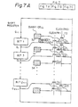
- FIG. 7 A semiconductor memory device according to an embodiment of the present invention is shown in Fig. 7.
- transfer gates T3 221 to 235 and T4 222 to 236 are provided.
- the odd column of shift register stage No. 1 to No. 7 and the even column of shift register stage No. 2 to No. 8 can be connected to the odd number bit lines (BL1, BL3, BL5, and BL7) and the even number bit lines (BL2, BL4, BL6, and BL8). Dummy cells are also connected to the odd and even number bit lines.
- the selection of transfer gates Tl to T4 is carried out by the exclusive transfer clocks TR1 and TR2. That is, if the clock TR2 is the L level and the clock TR1 is the H level, gates Tl and T2 turn on, just as in Fig.
- This inversion mode enables a one-bit shift. That is, in the inversion mode the coupling of the RAM and the shift register stages is inverted from odd to even or vice versa. For instance, the connection of the shift register stage No. 1 and bit line BL-1, shift register stage No. 2 and bit line BL-2, shift register stage No. 3 and bit line BL-3, and so on changes to connection of the shift register stage No. 1 and bit line BL-2, shift register stage No. 2 and bit line BL-3, shift register stage No. 3 and bit line BL-4, and so on. Therefore, after an intermediate shift by a master stage clock (Pl in Fig.
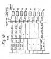
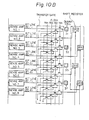
- Figure 10 shows an embodiment where the shift register is divided into four columns. Compared with Fig. 7, a multiplexer portion for the serial input S-IN and serial output S-OUT is omitted.
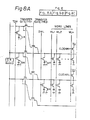
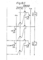
- Figure 8 is a view of another embodiment of the present invention. With regards to the bit lines WLn and WLn, a pair of active pull-up circuits are connected to the sense amplifier No. n. In other points, the operations of a shift register and transfer gates are the same as in Fig. 7.
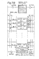
- Figure 9 is a view of the operation of a RAM.
- a reset signal R carries out precharging of bit lines (BL and BL).
- bit lines BL and BL.
- BL, BL, AP an active pull-up circuit
- ⁇ DWL,
- TR1, WL1, and TDW are shown.
- the upper portion and lower portion express the transfer from a RAM to a shift register and the transfer from a shift register to a RAM.
Landscapes
- Engineering & Computer Science (AREA)
- Microelectronics & Electronic Packaging (AREA)
- Computer Hardware Design (AREA)
- Databases & Information Systems (AREA)
- Dram (AREA)
- Static Random-Access Memory (AREA)
Applications Claiming Priority (2)
| Application Number | Priority Date | Filing Date | Title |
|---|---|---|---|
| JP216785/84 | 1984-10-16 | ||
| JP59216785A JPS6194295A (ja) | 1984-10-16 | 1984-10-16 | 半導体記憶装置 |
Publications (3)
| Publication Number | Publication Date |
|---|---|
| EP0178922A2 true EP0178922A2 (fr) | 1986-04-23 |
| EP0178922A3 EP0178922A3 (en) | 1988-03-30 |
| EP0178922B1 EP0178922B1 (fr) | 1990-06-13 |
Family
ID=16693848
Family Applications (1)
| Application Number | Title | Priority Date | Filing Date |
|---|---|---|---|
| EP85307459A Expired - Lifetime EP0178922B1 (fr) | 1984-10-16 | 1985-10-16 | Dispositif de mémoire semi-conductrice |
Country Status (5)
| Country | Link |
|---|---|
| US (1) | US4773045A (fr) |
| EP (1) | EP0178922B1 (fr) |
| JP (1) | JPS6194295A (fr) |
| KR (1) | KR900007996B1 (fr) |
| DE (1) | DE3578254D1 (fr) |
Cited By (6)
| Publication number | Priority date | Publication date | Assignee | Title |
|---|---|---|---|---|
| EP0361561A1 (fr) * | 1988-08-29 | 1990-04-04 | Koninklijke Philips Electronics N.V. | Circuit intégré de mémorisation muni d'une entrée et d'une sortie parallèles et série |
| WO1990007184A1 (fr) * | 1988-12-12 | 1990-06-28 | Eastman Kodak Company | Procede et appareil pour traiter des donnees rapides |
| EP0288774A3 (fr) * | 1987-04-30 | 1991-01-02 | International Business Machines Corporation | Circuit de bloc de registres à haute densité à haute performance |
| EP0479274A3 (en) * | 1990-10-02 | 1993-07-21 | Kabushiki Kaisha Toshiba | Semiconductor memory device |
| EP0479163A3 (en) * | 1990-09-29 | 1993-08-11 | Kabushiki Kaisha Toshiba | Semiconductor memory device |
| GB2374704A (en) * | 2001-04-18 | 2002-10-23 | Samsung Electronics Co Ltd | Serial data input to a non-volatile memory |
Families Citing this family (10)
| Publication number | Priority date | Publication date | Assignee | Title |
|---|---|---|---|---|
| US5200925A (en) * | 1988-07-29 | 1993-04-06 | Mitsubishi Denki Kabushiki Kaisha | Serial access semiconductor memory device and operating method therefor |
| DE3832328A1 (de) * | 1988-09-23 | 1990-03-29 | Broadcast Television Syst | Speicheranordnung fuer digitale signale |
| GB8925723D0 (en) * | 1989-11-14 | 1990-01-04 | Amt Holdings | Processor array system |
| US4984214A (en) * | 1989-12-05 | 1991-01-08 | International Business Machines Corporation | Multiplexed serial register architecture for VRAM |
| US8636648B2 (en) | 1999-03-01 | 2014-01-28 | West View Research, Llc | Endoscopic smart probe |
| US7914442B1 (en) | 1999-03-01 | 2011-03-29 | Gazdzinski Robert F | Endoscopic smart probe and method |
| US8068897B1 (en) | 1999-03-01 | 2011-11-29 | Gazdzinski Robert F | Endoscopic smart probe and method |
| US10973397B2 (en) | 1999-03-01 | 2021-04-13 | West View Research, Llc | Computerized information collection and processing apparatus |
| US10318903B2 (en) | 2016-05-06 | 2019-06-11 | General Electric Company | Constrained cash computing system to optimally schedule aircraft repair capacity with closed loop dynamic physical state and asset utilization attainment control |
| CN114097037B (zh) * | 2019-05-16 | 2025-01-07 | 艾克斯安耐杰克有限公司 | 可移位存储器和操作可移位存储器的方法 |
Family Cites Families (7)
| Publication number | Priority date | Publication date | Assignee | Title |
|---|---|---|---|---|
| US4151609A (en) * | 1977-10-11 | 1979-04-24 | Monolithic Memories, Inc. | First in first out (FIFO) memory |
| US4321695A (en) * | 1979-11-23 | 1982-03-23 | Texas Instruments Incorporated | High speed serial access semiconductor memory with fault tolerant feature |
| US4330852A (en) * | 1979-11-23 | 1982-05-18 | Texas Instruments Incorporated | Semiconductor read/write memory array having serial access |
| US4347587A (en) * | 1979-11-23 | 1982-08-31 | Texas Instruments Incorporated | Semiconductor integrated circuit memory device with both serial and random access arrays |
| US4281401A (en) * | 1979-11-23 | 1981-07-28 | Texas Instruments Incorporated | Semiconductor read/write memory array having high speed serial shift register access |
| US4412313A (en) * | 1981-01-19 | 1983-10-25 | Bell Telephone Laboratories, Incorporated | Random access memory system having high-speed serial data paths |
| JPS6194296A (ja) * | 1984-10-16 | 1986-05-13 | Fujitsu Ltd | 半導体記憶装置 |
-
1984
- 1984-10-16 JP JP59216785A patent/JPS6194295A/ja active Pending
-
1985
- 1985-10-16 EP EP85307459A patent/EP0178922B1/fr not_active Expired - Lifetime
- 1985-10-16 US US06/788,000 patent/US4773045A/en not_active Expired - Fee Related
- 1985-10-16 DE DE8585307459T patent/DE3578254D1/de not_active Expired - Lifetime
- 1985-10-16 KR KR1019850007619A patent/KR900007996B1/ko not_active Expired
Cited By (10)
| Publication number | Priority date | Publication date | Assignee | Title |
|---|---|---|---|---|
| EP0288774A3 (fr) * | 1987-04-30 | 1991-01-02 | International Business Machines Corporation | Circuit de bloc de registres à haute densité à haute performance |
| EP0361561A1 (fr) * | 1988-08-29 | 1990-04-04 | Koninklijke Philips Electronics N.V. | Circuit intégré de mémorisation muni d'une entrée et d'une sortie parallèles et série |
| WO1990007184A1 (fr) * | 1988-12-12 | 1990-06-28 | Eastman Kodak Company | Procede et appareil pour traiter des donnees rapides |
| EP0479163A3 (en) * | 1990-09-29 | 1993-08-11 | Kabushiki Kaisha Toshiba | Semiconductor memory device |
| US5295254A (en) * | 1990-09-29 | 1994-03-15 | Kabushiki Kaisha Toshiba | Semiconductor memory device cell array divided into a plurality of blocks |
| EP0479274A3 (en) * | 1990-10-02 | 1993-07-21 | Kabushiki Kaisha Toshiba | Semiconductor memory device |
| US5418745A (en) * | 1990-10-02 | 1995-05-23 | Kabushiki Kaisha Toshiba | Semiconductor memory device for continuously accessing a memory cell array divided according to a column address |
| GB2374704A (en) * | 2001-04-18 | 2002-10-23 | Samsung Electronics Co Ltd | Serial data input to a non-volatile memory |
| GB2374704B (en) * | 2001-04-18 | 2003-06-18 | Samsung Electronics Co Ltd | Method and device for programming nonvolatile semiconductor memory |
| US6915175B2 (en) | 2001-04-18 | 2005-07-05 | Samsung Electronics Co., Ltd. | Method and device for programming nonvolatile semiconductor memory |
Also Published As
| Publication number | Publication date |
|---|---|
| EP0178922B1 (fr) | 1990-06-13 |
| KR860003605A (ko) | 1986-05-28 |
| JPS6194295A (ja) | 1986-05-13 |
| EP0178922A3 (en) | 1988-03-30 |
| KR900007996B1 (ko) | 1990-10-23 |
| US4773045A (en) | 1988-09-20 |
| DE3578254D1 (de) | 1990-07-19 |
Similar Documents
| Publication | Publication Date | Title |
|---|---|---|
| EP0178922B1 (fr) | Dispositif de mémoire semi-conductrice | |
| EP0249548B1 (fr) | Dispositif de mémoire à semi-conducteurs à double porte | |
| US4899316A (en) | Semiconductor memory device having serial writing scheme | |
| US4567579A (en) | Dynamic memory with high speed nibble mode | |
| US5815444A (en) | Serial access system semiconductor storage device capable of reducing access time and consumption current | |
| KR960001972A (ko) | 단일 칩 프레임 버퍼 및 그래픽 가속기 | |
| KR940006362B1 (ko) | 반도체 기억장치와 그 동작방법 | |
| JPS61104391A (ja) | 半導体記憶装置 | |
| US4937788A (en) | Semiconductor memory circuit with improved serial access circuit arrangement | |
| EP0326172B1 (fr) | Circuit de mémoire avec un dispositif de circuit d'accés sériel | |
| EP0154379A2 (fr) | Arrangement de réseau pour des EEPROMS | |
| GB1519985A (en) | Computer momories | |
| JP3481263B2 (ja) | シリアル記憶装置 | |
| US5317540A (en) | Semiconductor memory device | |
| KR930004669B1 (ko) | 시리얼 액세스 메모리로 이루어진 반도체 기억장치 | |
| US5732026A (en) | Semiconductor memory device including main/sub-bit line arrangement | |
| KR890002773A (ko) | 디지탈 비데오 신호의 기억 장치 및 그 방법 | |
| JP3057747B2 (ja) | 半導体メモリ装置 | |
| US5267212A (en) | Random access memory with rapid test pattern writing | |
| IE53486B1 (en) | Memory | |
| US5349561A (en) | Multiport memory and method of operation thereof | |
| KR930000768B1 (ko) | 반도체 기억장치 | |
| US5625594A (en) | Digital video memory | |
| KR100282519B1 (ko) | 플래시 메모리의 데이터 리드속도 향상회로 | |
| JPH03105788A (ja) | 半導体記憶装置 |
Legal Events
| Date | Code | Title | Description |
|---|---|---|---|
| PUAI | Public reference made under article 153(3) epc to a published international application that has entered the european phase |
Free format text: ORIGINAL CODE: 0009012 |
|
| AK | Designated contracting states |
Kind code of ref document: A2 Designated state(s): DE FR GB |
|
| PUAL | Search report despatched |
Free format text: ORIGINAL CODE: 0009013 |
|
| RHK1 | Main classification (correction) |
Ipc: G11C 8/00 |
|
| AK | Designated contracting states |
Kind code of ref document: A3 Designated state(s): DE FR GB |
|
| 17P | Request for examination filed |
Effective date: 19880427 |
|
| 17Q | First examination report despatched |
Effective date: 19891009 |
|
| GRAA | (expected) grant |
Free format text: ORIGINAL CODE: 0009210 |
|
| AK | Designated contracting states |
Kind code of ref document: B1 Designated state(s): DE FR GB |
|
| REF | Corresponds to: |
Ref document number: 3578254 Country of ref document: DE Date of ref document: 19900719 |
|
| ET | Fr: translation filed | ||
| PLBE | No opposition filed within time limit |
Free format text: ORIGINAL CODE: 0009261 |
|
| STAA | Information on the status of an ep patent application or granted ep patent |
Free format text: STATUS: NO OPPOSITION FILED WITHIN TIME LIMIT |
|
| 26N | No opposition filed | ||
| PGFP | Annual fee paid to national office [announced via postgrant information from national office to epo] |
Ref country code: GB Payment date: 19920804 Year of fee payment: 8 |
|
| PGFP | Annual fee paid to national office [announced via postgrant information from national office to epo] |
Ref country code: FR Payment date: 19921028 Year of fee payment: 8 |
|
| PGFP | Annual fee paid to national office [announced via postgrant information from national office to epo] |
Ref country code: DE Payment date: 19921226 Year of fee payment: 8 |
|
| PG25 | Lapsed in a contracting state [announced via postgrant information from national office to epo] |
Ref country code: GB Effective date: 19931016 |
|
| GBPC | Gb: european patent ceased through non-payment of renewal fee |
Effective date: 19931016 |
|
| PG25 | Lapsed in a contracting state [announced via postgrant information from national office to epo] |
Ref country code: FR Effective date: 19940630 |
|
| PG25 | Lapsed in a contracting state [announced via postgrant information from national office to epo] |
Ref country code: DE Effective date: 19940701 |
|
| REG | Reference to a national code |
Ref country code: FR Ref legal event code: ST |