EP0178992A2 - Configuration du circuit de source de tension d'alimentation double pour un circuit de ligne téléphonique - Google Patents
Configuration du circuit de source de tension d'alimentation double pour un circuit de ligne téléphonique Download PDFInfo
- Publication number
- EP0178992A2 EP0178992A2 EP85401986A EP85401986A EP0178992A2 EP 0178992 A2 EP0178992 A2 EP 0178992A2 EP 85401986 A EP85401986 A EP 85401986A EP 85401986 A EP85401986 A EP 85401986A EP 0178992 A2 EP0178992 A2 EP 0178992A2
- Authority
- EP
- European Patent Office
- Prior art keywords
- line
- voltage source
- hook
- coupled
- circuit
- Prior art date
- Legal status (The legal status is an assumption and is not a legal conclusion. Google has not performed a legal analysis and makes no representation as to the accuracy of the status listed.)
- Granted
Links
Images

Classifications
-
- H—ELECTRICITY
- H04—ELECTRIC COMMUNICATION TECHNIQUE
- H04M—TELEPHONIC COMMUNICATION
- H04M19/00—Current supply arrangements for telephone systems
- H04M19/001—Current supply source at the exchanger providing current to substations
- H04M19/008—Using DC/DC converters
Definitions
- the present invention generally relates to telephone line circuits and, in particular, relates to a feed circuit for such a telephone line circuit employing a floating voltage supply together with the standard central office voltage supply.
- a wideband high voltage and high power amplifier that employs a switching converter with the capacitor storage element coupled across a subscriber line is described.
- the subscriber line is characterized as having a definite load impedance that is mainly resistive and appears in parallel with the storage capacitor of the switching converter.
- one object of the present invention is to provide line feed circuit configuration that may be employed in a line circuit to substantially reduce power dissipation and to improve operation.
- a line circuit including a selectively operated voltage source coupled across the line and operative to supply an auxiliary operating current thereto.
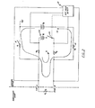
- FIG. 1 there is shown a schematic diagram of a line circuit utilizing a floating DC source 10 also designated as V A
- the resistor 11 constitutes the line impedance and is conventionally designated as R L .
- the line impedance of a subscriber line, in the off hook condition, is a function of the length of a subscriber line, and the typical impedance of such lines may vary between a very low value to over 2000 ohms or more.
- the floating DC source 10 is coupled to the line terminals A and B via equal resistors 12 and 13 designated as R B .
- the terminals A and B, on the respective sides of a subscriber line, are also referred to as the ring, or R, side and the tip, or T, side of the line.
- the central office battery conventionally supplied by the switching system, is designated as V B and often varies between 48 to 60 volts depending on the particular telephone exchange.
- the central office battery is supplied to the line circuit terminals via the feed resistors 14 and 15.
- the office battery V B is the regular central office battery and the floating DC source 10, for example, is a switching DC/DC converter that can be employed for line supervision and line feed respectively.
- the converter 10 in the on hook state, is turned off and the off hook supervision is performed solely by the central office battery V B .
- the turning off of the floating voltage supply V A is accomplished by means of the switch 20 effectively in series with the V A supply as shown in Figure 1.
- the voltage source V A can be structured to be an amplifier having a bandwidth and power capability enabling it to handle DC, ringing, voice and remote metering signals having a frequency of, for example, between 12 to 16 KH Z . In this manner the amplifier is a single device capable of handling all of the basic driving functions of the line circuit.
- the amplifier can have the basic structure of a switching type converter.
- V 1 and V 2 the voltages at the junctions between resistors, 12 and 15, and resistors, 13 and 14, denoted as V 1 and V 2 respectively, are as follows:
- V 1 and V 2' When the switch 20 is closed the voltages, V 1 and V 2' can be shown to be as follows:
- the central office battery When switch 20 is open, as for example in the on hook state, the central office battery performs the off hook supervision.
- the resistors, 12 and 13, are selected to be in the range of 25 to 200 ohms, while the resistors R 1 are in the range of 5,400 to 50,000 ohms.
- the voltage source 10 is turned off by the equivalent of opening up switch 20.
- the voltage source 10 is a DC/DC converter or amplifier.
- the central office battery V B is used mainly to detect the off hook condition.
- the floating supply 10 is turned on in the off hook state to provide talk current to the loop.
- an off hook detector 25 senses the loop current (I 2 ) due to the subscriber line going off hook and upon detection of this condition operates switch 20 to place the voltage source 10 (V A ) in circuit and cause an additional loop current (I 1 ) to flow.
- the additional loop current supplies the necessary talk current to the line.
- This turn-on operation in a system environment, can be executed by the software of such a system.
- the off hook detector 25 is a conventional circuit configuration and senses the current flow in the two-wire line due to the subscriber going off hook and furnished by the central office battery Y B .
- FIG 2 there is shown a similar circuit as Figure 1 wherein the central office battery is connected to the line terminals A and B, or the tip and ring terminals, via resistors R 1 and R 2 designated as 21 and 22, respectively.
- resistors are auxiliary feed resistors for the central office battery. If one compares the circuit of Figure 1 with the circuit of Figure 2, one can see that the floating source 10 is under the control of switch 20 with the major difference between the circuits residing in the portion of the central office battery V B .
- auxiliary voltage source includes a switching converter amplifier configuration.
- Such amplifier configurations have been extensively described in the above noted co-pending application, A WIDEBAND HIGH VOLTAGE AMPLIFIER FOR TELEPHONE EXCHANGE SUBSCRIBER LINE INTERFACE UTILIZING LOW VOLTAGE CIRCUITRY filed April 10, 1984 as Serial Number 598,650 by R. C. W. Chea, Jr. and assigned to the assignee hereof.
- the subscriber line which is normally associated with a subscriber subset 30 is coupled to the tip (T) and ring (R) lines by means of the feed resistors 31 and 32 designated as R B .
- the subscriber line constitutes a two-wire line of a length depending upon the distance of the line from the central office and is manifested in having a definite impedance 33 which is mainly a resistive component and designated as R L .
- the central office battery V is coupled to the line by means of resistors, 34 and 35, designated as R 1 which resistors are much greater in magnitude than resistors 31 and 34.
- resistors, 34 and 35 would be about 20,000 ohms, while resistors 31 and 32 would be about 100 ohms.
- the subscriber subset 30, data terminal or other device is normally associated with a hook switch (HS) 36.
- the off hook detector is operative to detect a current flow in the subscriber line which is indicative of the closing of the hook switch 36.
- the initial loop current is supplied by the central office battery V B .
- the auxiliary voltage VA is impressed upon the line to provide talk current to the loop and to provide the other features as the ringing, voltage and so on to the loop. In this manner the subscriber line is efficiently operated.
- the on hook state is the predominate state.
- a subscriber line is mainly on hook during most of the day.
- the auxiliary voltage source is activated and additional current is supplied to the loop to provide an optimum talk current.
- reference numeral 10 designates the switching converter portion of the amplifier circuit.
- the switching converter 10 as included within the dashed lines is a relatively standard component.
- a capacitor 41 is shunted across the subscriber line and is fed from a diode 42 which is coupled to the secondary of a power transformer 43.
- the primary of the power transformer 43 has one terminal coupled to the central office battery V B and another terminal coupled to ground through an FET.
- An amplifier 52 which is a buffer amplifier has one input terminal coupled to the junction between resistors 31 and 35 and another input terminal coupled to the junction between resistors, 32 and 34.
- the output of the amplifier 52 is coupled to one input of a summer 53. Another input to the summer is designated as V in and is the input signal terminal for the line circuit.
- the signal V in may constitute the ringing signal, the talk signal or a high frequency metering signal.
- Such signals as applied to line circuits are well known.
- the output of the summer is coupled to the input of a second amplifier 54 which provides gain and frequency shaping for the switching converter amplifier as necessitated by the line circuit.
- the output of amplifier 54 is coupled to one input of a pulse width modulator 55 which has another input coupled to a reference voltage or clock source 56.
- the pulse width modulator SS may include a comparator employing, for example, a triangular wave shape reference source.
- the output of the pulse width modulator 55 is coupled to the gate electrode of the FET 44.
- the FET 44 has its source and drain electrodes coupled in series with the primary winding of the power transformer 43.
- the secondary winding of the power transformer 43 as indicated, has one terminal coupled to the anode of the diode 42 with the cathode of the diode coupled to the junction between resistor 31 and capacitor 41.
- the capacitor 41 is shunted across the subscriber line.
- the voltage across the capacitor i.e., the auxiliary voltage source, is a function of the operation of the pulse width modulator as controlled by the gating of the FET 44.
- each of the various modules such as amplifiers 52 and 54, the pulse width modulator 55, the clock source and so on must receive an operating potential.
- one way of implementing operation of the amplifier, including the switching converter is to supply the source voltage for the above components through an additional switching device such as an FET.
- the gate electrode thereof is coupled to the output of the off hook detector 40.
- the FET is turned on to supply bias to the various modules coupled thereto.
- the FET is biased in a high impedance state and the amplifier configuration described does not operate and does not consume power.
- the entire amplifier is completely inactive in the on hook state, and apart from the fact that there is no power dissipation, there is also no high frequency noise generated due to the normal operating conditions of the switching converter.
- the amplifier incorporating the switching converter is only active after the off hook condition is detected, and during this time, the auxiliary voltage source generates the voltage V A to supply the proper line feed current to the line circuit.
- the entire amplifier circuit as explained in the co-pending application is operative to handle DC, ringing, voice and remote metering signals.
Landscapes
- Engineering & Computer Science (AREA)
- Signal Processing (AREA)
- Devices For Supply Of Signal Current (AREA)
- Interface Circuits In Exchanges (AREA)
- Telephone Function (AREA)
- Sub-Exchange Stations And Push- Button Telephones (AREA)
Priority Applications (1)
| Application Number | Priority Date | Filing Date | Title |
|---|---|---|---|
| AT85401986T ATE47946T1 (de) | 1984-10-15 | 1985-10-14 | Zweifachspeisespannungsschaltungsstruktur fuer eine fernsprechleitungsschaltung. |
Applications Claiming Priority (2)
| Application Number | Priority Date | Filing Date | Title |
|---|---|---|---|
| US06/660,585 US4602130A (en) | 1984-10-15 | 1984-10-15 | Dual voltage source feed circuit configuration for a telephone line circuit |
| US660585 | 1984-10-15 |
Publications (3)
| Publication Number | Publication Date |
|---|---|
| EP0178992A2 true EP0178992A2 (fr) | 1986-04-23 |
| EP0178992A3 EP0178992A3 (en) | 1987-02-25 |
| EP0178992B1 EP0178992B1 (fr) | 1989-11-08 |
Family
ID=24650127
Family Applications (1)
| Application Number | Title | Priority Date | Filing Date |
|---|---|---|---|
| EP85401986A Expired EP0178992B1 (fr) | 1984-10-15 | 1985-10-14 | Configuration du circuit de source de tension d'alimentation double pour un circuit de ligne téléphonique |
Country Status (6)
| Country | Link |
|---|---|
| US (1) | US4602130A (fr) |
| EP (1) | EP0178992B1 (fr) |
| JP (1) | JPS6196861A (fr) |
| AT (1) | ATE47946T1 (fr) |
| AU (1) | AU584125B2 (fr) |
| ES (1) | ES8704058A1 (fr) |
Cited By (1)
| Publication number | Priority date | Publication date | Assignee | Title |
|---|---|---|---|---|
| GB2337179A (en) * | 1998-05-08 | 1999-11-10 | Bell Atlantic Corp | Power feed circuit |
Families Citing this family (3)
| Publication number | Priority date | Publication date | Assignee | Title |
|---|---|---|---|---|
| US4761812A (en) * | 1985-12-10 | 1988-08-02 | U.S. Holding Company, Inc. | Constant power telephone line circuit |
| SE9300941L (sv) * | 1993-03-22 | 1994-09-23 | Rosengren Teknik Ab | Anordning för sammankoppling av två apparater försedda med telelinjeanslutning |
| US5659610A (en) * | 1994-09-28 | 1997-08-19 | Lucent Technologies Inc. | Battery feed circuit |
Family Cites Families (13)
| Publication number | Priority date | Publication date | Assignee | Title |
|---|---|---|---|---|
| US4142075A (en) * | 1977-10-11 | 1979-02-27 | Burr-Brown Research Corporation | Interface circuit and method for telephone extension lines |
| NL7807531A (nl) * | 1978-07-13 | 1980-01-15 | Philips Nv | Inrichting voor het toevoeren van een signaal aan een transmissielijn. |
| US4254305A (en) * | 1979-02-07 | 1981-03-03 | International Telephone And Telegraph Corporation | Current limited subscriber line feed circuit |
| NL7903662A (nl) * | 1979-05-10 | 1980-11-12 | Philips Nv | Lijncircuit. |
| US4315106A (en) * | 1979-11-28 | 1982-02-09 | International Telephone And Telegraph Corporation | Apparatus for regulating current supplied to a telephone line signal of the type employed in digital telephone systems |
| GB2065418B (en) * | 1979-12-06 | 1984-02-15 | Standard Telephones Cables Ltd | Telephone line feed |
| US4387273A (en) * | 1980-08-25 | 1983-06-07 | International Telephone And Telegraph Corporation | Subscriber line interface circuit with impedance synthesizer |
| DE3264466D1 (en) * | 1981-01-28 | 1985-08-08 | Hitachi Ltd | Current supply circuit |
| CA1157175A (fr) * | 1981-02-20 | 1983-11-15 | Mitel Corporation | Circuit economiseur d'energie pour ligne |
| JPS5883492A (ja) * | 1981-11-12 | 1983-05-19 | Nec Corp | 加入者回路の低電力化方式 |
| US4514595A (en) * | 1982-06-10 | 1985-04-30 | Northern Telecom Limited | Active impedance line feed circuit |
| US4511763A (en) * | 1982-11-01 | 1985-04-16 | Gte Communication Systems Corporation | Floating dc current source for a subscriber loop circuit |
| US4499532A (en) * | 1983-03-23 | 1985-02-12 | At&T Bell Laboratories | Floating battery feed circuit |
-
1984
- 1984-10-15 US US06/660,585 patent/US4602130A/en not_active Expired - Fee Related
-
1985
- 1985-10-03 AU AU48234/85A patent/AU584125B2/en not_active Ceased
- 1985-10-14 AT AT85401986T patent/ATE47946T1/de not_active IP Right Cessation
- 1985-10-14 EP EP85401986A patent/EP0178992B1/fr not_active Expired
- 1985-10-15 ES ES547883A patent/ES8704058A1/es not_active Expired
- 1985-10-15 JP JP60227952A patent/JPS6196861A/ja active Pending
Cited By (2)
| Publication number | Priority date | Publication date | Assignee | Title |
|---|---|---|---|---|
| GB2337179A (en) * | 1998-05-08 | 1999-11-10 | Bell Atlantic Corp | Power feed circuit |
| GB2337179B (en) * | 1998-05-08 | 2003-10-22 | Bell Atlantic Corp | Power feed circuit providing both on-hook and off-hook power for telephone for telephone subscriber loop |
Also Published As
| Publication number | Publication date |
|---|---|
| AU4823485A (en) | 1986-04-24 |
| US4602130A (en) | 1986-07-22 |
| ES8704058A1 (es) | 1987-02-16 |
| EP0178992A3 (en) | 1987-02-25 |
| EP0178992B1 (fr) | 1989-11-08 |
| AU584125B2 (en) | 1989-05-18 |
| JPS6196861A (ja) | 1986-05-15 |
| ATE47946T1 (de) | 1989-11-15 |
| ES547883A0 (es) | 1987-02-16 |
Similar Documents
| Publication | Publication Date | Title |
|---|---|---|
| US5737411A (en) | Battery switching in a telephone subscriber line interface circuit | |
| EP0178993B1 (fr) | Configuration du circuit d'entrée pour un circuit d'interface d'une ligne d'abonné | |
| US4056689A (en) | Telephone subscriber line circuit | |
| US4056691A (en) | Telephone subscriber line circuit | |
| EP0178992B1 (fr) | Configuration du circuit de source de tension d'alimentation double pour un circuit de ligne téléphonique | |
| EP0102111B1 (fr) | Circuit pour téléphone | |
| US7076055B2 (en) | Tracking switchmode power converter for telephony interface circuit | |
| US4896352A (en) | Telephone set circuit including an overvoltage protection | |
| GB2262668A (en) | Battery charging device for a portable telephone | |
| EP0425675B1 (fr) | Circuit de detection de defaut de connexion a la terre pour lignes d'abonnes | |
| US6104791A (en) | System and method for performing telephone line-in-use detection, extension pick-up detection, and remote hang-up detection in a modem | |
| US4234762A (en) | Ring trip detector circuit | |
| AU606397B2 (en) | Telephone subset circuit arrangement | |
| JP2668688B2 (ja) | 通信システムの端末装置 | |
| US4609782A (en) | Solid state signal insertion circuit and method for use in a telephony system or the like | |
| KR100365577B1 (ko) | 전화훅스위치인터페이스회로 | |
| US4388497A (en) | Telephone power supply arrangement | |
| USRE35582E (en) | Subscriber line interface circuit with power-down mode | |
| US5859906A (en) | Telephone switch hook interface circuit | |
| US4552994A (en) | Apparatus for isolating the voice frequency path from the floating battery feed during signalling | |
| KR890000592B1 (ko) | 전화기의 뮤직 온 홀드(Music On Hold)기능 제어스위칭 회로 | |
| US6842520B2 (en) | Telephone | |
| JPH0662445A (ja) | 過電圧保護回路 | |
| KR980013465A (ko) | 가입자 선로 인터페이스 회로 | |
| JPS603296A (ja) | 電子式ボタン電話装置 |
Legal Events
| Date | Code | Title | Description |
|---|---|---|---|
| PUAI | Public reference made under article 153(3) epc to a published international application that has entered the european phase |
Free format text: ORIGINAL CODE: 0009012 |
|
| AK | Designated contracting states |
Kind code of ref document: A2 Designated state(s): AT FR GB IT NL SE |
|
| PUAL | Search report despatched |
Free format text: ORIGINAL CODE: 0009013 |
|
| AK | Designated contracting states |
Kind code of ref document: A3 Designated state(s): AT FR GB IT NL SE |
|
| 17P | Request for examination filed |
Effective date: 19870403 |
|
| RAP1 | Party data changed (applicant data changed or rights of an application transferred) |
Owner name: ALCATEL N.V. |
|
| RAP3 | Party data changed (applicant data changed or rights of an application transferred) |
Owner name: ALCATEL N.V. |
|
| 17Q | First examination report despatched |
Effective date: 19880816 |
|
| ITF | It: translation for a ep patent filed | ||
| GRAA | (expected) grant |
Free format text: ORIGINAL CODE: 0009210 |
|
| AK | Designated contracting states |
Kind code of ref document: B1 Designated state(s): AT FR GB IT NL SE |
|
| REF | Corresponds to: |
Ref document number: 47946 Country of ref document: AT Date of ref document: 19891115 Kind code of ref document: T |
|
| ET | Fr: translation filed | ||
| PLBE | No opposition filed within time limit |
Free format text: ORIGINAL CODE: 0009261 |
|
| STAA | Information on the status of an ep patent application or granted ep patent |
Free format text: STATUS: NO OPPOSITION FILED WITHIN TIME LIMIT |
|
| PGFP | Annual fee paid to national office [announced via postgrant information from national office to epo] |
Ref country code: GB Payment date: 19900919 Year of fee payment: 6 |
|
| PGFP | Annual fee paid to national office [announced via postgrant information from national office to epo] |
Ref country code: SE Payment date: 19900926 Year of fee payment: 6 Ref country code: FR Payment date: 19900926 Year of fee payment: 6 |
|
| PGFP | Annual fee paid to national office [announced via postgrant information from national office to epo] |
Ref country code: AT Payment date: 19901011 Year of fee payment: 6 |
|
| 26N | No opposition filed | ||
| ITTA | It: last paid annual fee | ||
| PGFP | Annual fee paid to national office [announced via postgrant information from national office to epo] |
Ref country code: NL Payment date: 19901031 Year of fee payment: 6 |
|
| PG25 | Lapsed in a contracting state [announced via postgrant information from national office to epo] |
Ref country code: GB Effective date: 19911014 Ref country code: AT Effective date: 19911014 |
|
| PG25 | Lapsed in a contracting state [announced via postgrant information from national office to epo] |
Ref country code: SE Effective date: 19911015 |
|
| PG25 | Lapsed in a contracting state [announced via postgrant information from national office to epo] |
Ref country code: NL Effective date: 19920501 |
|
| GBPC | Gb: european patent ceased through non-payment of renewal fee | ||
| NLV4 | Nl: lapsed or anulled due to non-payment of the annual fee | ||
| PG25 | Lapsed in a contracting state [announced via postgrant information from national office to epo] |
Ref country code: FR Effective date: 19920630 |
|
| REG | Reference to a national code |
Ref country code: FR Ref legal event code: ST |
|
| EUG | Se: european patent has lapsed |
Ref document number: 85401986.6 Effective date: 19920510 |