EP0179605A2 - Dispositif de mémoire semi-conductrice avec un circuit d'entrée et de sortie séquentielle d'informations - Google Patents
Dispositif de mémoire semi-conductrice avec un circuit d'entrée et de sortie séquentielle d'informations Download PDFInfo
- Publication number
- EP0179605A2 EP0179605A2 EP85307355A EP85307355A EP0179605A2 EP 0179605 A2 EP0179605 A2 EP 0179605A2 EP 85307355 A EP85307355 A EP 85307355A EP 85307355 A EP85307355 A EP 85307355A EP 0179605 A2 EP0179605 A2 EP 0179605A2
- Authority
- EP
- European Patent Office
- Prior art keywords
- data
- circuit
- gate
- shift register
- gates
- Prior art date
- Legal status (The legal status is an assumption and is not a legal conclusion. Google has not performed a legal analysis and makes no representation as to the accuracy of the status listed.)
- Granted
Links
Images


Classifications
-
- G—PHYSICS
- G11—INFORMATION STORAGE
- G11C—STATIC STORES
- G11C11/00—Digital stores characterised by the use of particular electric or magnetic storage elements; Storage elements therefor
- G11C11/21—Digital stores characterised by the use of particular electric or magnetic storage elements; Storage elements therefor using electric elements
- G11C11/34—Digital stores characterised by the use of particular electric or magnetic storage elements; Storage elements therefor using electric elements using semiconductor devices
-
- G—PHYSICS
- G11—INFORMATION STORAGE
- G11C—STATIC STORES
- G11C7/00—Arrangements for writing information into, or reading information out from, a digital store
- G11C7/10—Input/output [I/O] data interface arrangements, e.g. I/O data control circuits, I/O data buffers
- G11C7/1078—Data input circuits, e.g. write amplifiers, data input buffers, data input registers, data input level conversion circuits
- G11C7/1087—Data input latches
-
- G—PHYSICS
- G11—INFORMATION STORAGE
- G11C—STATIC STORES
- G11C11/00—Digital stores characterised by the use of particular electric or magnetic storage elements; Storage elements therefor
- G11C11/21—Digital stores characterised by the use of particular electric or magnetic storage elements; Storage elements therefor using electric elements
- G11C11/34—Digital stores characterised by the use of particular electric or magnetic storage elements; Storage elements therefor using electric elements using semiconductor devices
- G11C11/40—Digital stores characterised by the use of particular electric or magnetic storage elements; Storage elements therefor using electric elements using semiconductor devices using transistors
-
- G—PHYSICS
- G11—INFORMATION STORAGE
- G11C—STATIC STORES
- G11C7/00—Arrangements for writing information into, or reading information out from, a digital store
- G11C7/10—Input/output [I/O] data interface arrangements, e.g. I/O data control circuits, I/O data buffers
- G11C7/1051—Data output circuits, e.g. read-out amplifiers, data output buffers, data output registers, data output level conversion circuits
-
- G—PHYSICS
- G11—INFORMATION STORAGE
- G11C—STATIC STORES
- G11C7/00—Arrangements for writing information into, or reading information out from, a digital store
- G11C7/10—Input/output [I/O] data interface arrangements, e.g. I/O data control circuits, I/O data buffers
- G11C7/1075—Input/output [I/O] data interface arrangements, e.g. I/O data control circuits, I/O data buffers for multiport memories each having random access ports and serial ports, e.g. video RAM
-
- G—PHYSICS
- G11—INFORMATION STORAGE
- G11C—STATIC STORES
- G11C7/00—Arrangements for writing information into, or reading information out from, a digital store
- G11C7/10—Input/output [I/O] data interface arrangements, e.g. I/O data control circuits, I/O data buffers
- G11C7/1078—Data input circuits, e.g. write amplifiers, data input buffers, data input registers, data input level conversion circuits
Definitions
- This invention relates to a semiconductor memory device, and more particularly to a semiconductor memory device having a serial data input circuit and a serial data output circuit. It also relates to a semiconductor memory device which is operable as a high-speed data first-in first-out (FIFO) memory.
- FIFO data first-in first-out
- An image data processing system or the like requires a large-capacity memory.
- a dynamic random-access memory RAM
- a dynamic random-access memory RAM
- CRT cathode ray tube
- high-speed data storage and/or read-out are also required.
- a normal semiconductor memory device having a dynamic RAM suffers from the disadvantage of having low-speed data storage and/or read-out.
- a shift register set is used for data storage into, and/or data read-out from, the dynamic RAM of group data, e.g. 256 bits, thereby shortening the data storage and/or data read-out time.
- a data FIFO system for functioning as a register is known. This, however, suffers from the disadvantage of handling only a small amount of data.
- a data FIFO system for performing group data accessing of the memory cells is also known. The latter also suffers from a disadvantage of low processing speed.
- a semiconductor memory device comprising a memory cell array including a plurality of memory cells arranged in a matrix form with a plurality of bit lines and a plurality of word lines; characterised by
- the data buses include l, data bus lines, "R” being a positive number and a power of 2.
- the gate driving circuit preferably includes j/k shift registers, "j" being the number of bit lines.
- the semiconductor memory device may further include a circuit for counting the number of inputs of the serial input data into the shift register set and for outputting the counted value to the data output circuit.
- the gate driving circuit then drives one of the gates in the third gate set, in response to the counted value, to read-out data, from first to last, stored in the memory cells through the shift register set.
- the semiconductor memory device may further include a circuit for recording the sequence of selected word lines during the data storing operation from the serial data input circuit and selecting the word lines in response to the sequence of selected word lines during the data read operation by the serial data output circuit.
- the counting circuit counts the input number during the data store operation and outputs the counted value to the data output circuit.
- the gate driving 5 circuit performs the driving in response to each of the word line selections of the word line record and selection circuit.
- Figure 1 is a circuit diagram of a prior art semiconductor memory device comprising a dynamic RAM cell array 1 consisting of a plurality of dynamic memory cells arranged in a matrix form, and a row decoder 5 for selecting word lines WL 0 to WL 255 , connected to the memory cell array 1, in response to a row-address signal RA 0 to RA7-
- the device further comprises a sense amplifier set 2 consisting of a plurality of sense amplifiers SA 0 to Sp 255 connected to pairs of bit lines BL 0 : BL 0 to RL 255 :BL 255 connected to the memory cell array 1, a gate set 3 consisting of a plurality of gates connected to outputs of the sense amplifiers SA 0 to SA255, a column decoder 4 for selecting one of the gates in the gate set 3 in response to a column address signal CA 0 to CA 7 , a data bus (DB) 26 connected to the gates of the gate set 3, one of which may be selected in accordance with the output of the column decode
- the above-mentioned construction is the same as that of an extensively known dynamic RAM device and, accordingly, the basic operation thereof is similar.
- the above-mentioned circuits are referred to as the "dynamic RAM side" in the specification.
- the semiconductor memory device further includes a transfer gate set 20 consisting of a plurality of transfer gates TG 0 to TG 255 connected to the bit lines BL 0 to BL 255 , a shift register set 21 consisting of a plurality of shift registers SR 0 to SR 255 connected to the transfer gates TG 0 to TG 255 , an input amplifier 22 provided at an input side of the shift register set 21, and an output amplifier 23 provided at an output side of the shift register set 21.
- a transfer gate set 20 consisting of a plurality of transfer gates TG 0 to TG 255 connected to the bit lines BL 0 to BL 255
- a shift register set 21 consisting of a plurality of shift registers SR 0 to SR 255 connected to the transfer gates TG 0 to TG 255
- an input amplifier 22 provided at an input side of the shift register set 21
- an output amplifier 23 provided at an output side of the shift register set 21.
- All of the transfer gates TG 0 to TG 255 of the transfer gate set 20 are driven by a transfer clock signal TCLK output from a transfer clock driver 24, which signal is generated in accordance with a transfer request TR and a read or write command R/W applied to the transfer clock driver 24.
- the latter circuits are referred to as the "shift register side" in the specification.
- the dynamic RAM side and the shift register side are independently operable in a normal state.
- all of the transfer gates TG 0 to TG 255 are turned ON in response to the transfer clock signal TCLK to connect the respective shift registers SR 0 to SR 255 to the corresponding bit lines BL 0 to BL 255 .
- values stored in the 256 shift registers SR 0 to SR 255 are stored in a group in those memory cells in the memory cell array 1 decided upon by a certain word line.
- values stored in the 256 memory cells in the memory cell array 1 decided by a certain word line are read out, also in a group to the shift registers SR 0 to SR255.
- the shift register side and the dynamic RAM side are operable asynchronously, 256 bits of data may be input or output by the shift registers concurrently with a random access operation.
- the shift register side enables an improved serial access operation with approximately ten times the random access speed of the dynamic RAM side. It enables high-speed serial data output from the dynamic RAM cell array 1 storing, for example, image information to a CRT display unit, by transferring the image information for all word lines WL in a group, or high-speed serial data store from the CPU or I/O unit to the dynamic RAM cell array 1.
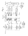
- Figure 2 is a circuit diagram of another prior art semiconductor memory device.
- the semiconductor memory device shown in Fig. 2 has a shift register side consisting of two transfer gate sets 20a and 20b, each of 256 transfer gates, two shift register sets 21a and 21b, each of 256 shift registers SRA 0 to SRA 255 and SRB 0 to SRB 255 , two input amplifiers 22a and 22b, and two output amplifiers 23a and 23b.
- the semiconductor memory device shown in Fig. 2 increases the serial access speed on the shift register side approximately two times more effectively than the device shown in Fig. 1 with the same speed shift clock pulse.
- shift registers are disadvantageous in view of lowering the integration of the semiconductor memory device. This problem is aggravated in that the shift registers are usually formed in the narrow space near the sense amplifiers and in parallel to the word lines and formation thereof requires a large area, resulting in a large area taken on the semiconductor chip. Furthermore, it increases the number of pins.
- Figure 3 is a circuit diagram of an embodiment of a semiconductor memory device in accordance with the present invention.
- the semiconductor memory device includes a dynamic RAM cell array 1, a row decoder 5, a sense amplifier set 2, a gate set 3, and a column decoder 4, identical to those in Figs. 1 and 2.
- the semiconductor memory device includes, at an input data side, an input transfer gate set 14a, a shift register set 15a, and an input amplifier 16a applied with an input data S IN .
- the semiconductor memory device also includes, at an output side, an output transfer gate set 12a, a latch circuit set 7a, an output gate set lla, a pointer shift register set 9a, a column decoder 10a designating the pointer shift register set 9a, a data bus 26 connected to the output gate set lla, and an output amplifier 13a connected to the data bus 26.
- the semiconductor memory device includes a transfer clock driver 6a outputting a A-phase transfer clock signal TCLKA for driving the output transfer gate set 12a and a B-phase transfer clock signal TCLKB for driving the input transfer gate set 14a.
- the dynamic RAM cell array 1 is defined by 256 word lines WL 0 to WL 255 and 256 bit lines BL 0 to BL 255' Accordingly, the input transfer gate set 14a consists of 256 gates.
- the shift register set 15a consists of 256 shift registers SR O to SR 255 for storing data to be written into the RAM cell array.
- the output transfer gate set 12a also consists of 256 gates.
- the latch circuit set 7a consists of 256 flip-flops FF 1 to FF 255 .
- the output gate set lla consists of 256 gates.
- the pointer shift register set 9a consists of 256 pointer registers.
- Figure 4 is a circuit diagram of a part of one example of the shift register set 15a shown in Fig. 3.
- the shift registers SR 0 and SR 1 shown in Fig. 4 are two- phase ratio-type shift registers.
- Figure 5 shows waveforms of the clock signal for driving the shift register set 15a of the type as shown in Fig. 4.
- a master mode a value at a node N 14 in the preceding shift register SR 0 is transferred in a node N 21 in the shift register SR1 by turning a transistor Q22 ON with a first clock pulse P 1 .
- the level at the node N 21 is high, i.e., logical "1"
- the level at a node N 22 is inverted by turning a transistor Q24 ON.
- a slave mode by applying a second clock pulse P 2 to a base of a transistor Q 26 , the transistor Q 26 is turned ON, with a resultant equal logic level between the nodes N 22 and N 23 .
- the level at a node N 24 may be inverted in accordance with the level at the node N 23 .
- the above successive operation in the shift register may be similarly applied to other shift registers in the shift register set 15a. As a result, one bit is consecutively shifted through the shift register set 15 in response to application of each pair of the clock signals P 1 and P 2 .
- shift registers for example, a conventional four-phase ratio-less type shift register, may be employed as the shift register set 15a, insofar as the registers are capable of storing and serially shifting data.
- Figure 6 is a specific circuit diagram of one circuit unit of the latch circuit set 7a, the output gate set lla, and the output transfer gate set 12a shown in Fig. 3.
- a pair of complementary bit lines BLi and BLi correspond to one bit line BL i in Fig. 3.
- One gate of the output transfer gate set 12a consists of transistors Q 36 and Q 37 connected to the pair of complementary bit lines BL i and BL i and driven by the A-phase clock signal TCLKA.
- One gate of the output gate set lla consists of transistors Q 30 and Q 32 connected to the data bus 26 formed by a pair of complementary data buses DB and DB.
- One latch circuit of the latch circuit set 7a consists of a pair of transistors Q 34 and Q 35 and a pair of capacitors C1 and C 2 to form a flip-flop circuit.
- the capacitors C 1 and C 2 may be formed by gate parasitic capacitances of the transistors Q 34 and Q 35 .
- Transistors Q 31 and Q 33 are buffer transistors for connecting outputs at nodes SQ and SQ of the flip-flop to the data bus 26.
- the operation of the circuits shown in Fig. 6 is as follows: (a) by applying the clock signal TCLKA, the transistors Q 36 and Q 37 are turned ON in a short period to introduce signals on the bit lines BL i and BL i to the nodes SQ and SQ, (b) in accordance with signal levels at the nodes SQ and SQ, the flip-flop 7a is set or reset and maintains its state and, at the same time, the buffer transistors Q33 and Q31 are turned ON or OFF in response to the signal level at the nodes SQ and SQ, and (c) by applying a pointer command PO i from one pointer shift register in the pointer register set 9a, the gate transistors Q 32 and Q 30 are turned ON in a short period to output the signals at the nodes SQ and SQ in the flip-flop to the pair of data buses DB and DB, with a resultant read-out of differential voltage between the data buses DB and DB at the output amplifier 13a.
- Figure 7 is another specific circuit diagram of a circuit unit, corresponding to that shown in Fig. 6.
- one bit line BL i is used.
- the gate of the output transfer gate set 12a consists of only one transistor Q 47 .
- the gate of the output gate set lla consists of transistors Q 40 and Q 42 .
- the flip-flop circuit 7a includes a charge-up transistor Q 44 in addition to the flip-flop circuit shown in Fig. 6.
- the transistors Q 45 and Q 46 , capacitors C 3 and C 4 , and buffer transistors Q41 and Q 43 correspond to the transistors Q 34 and Q35 , the capacitors C 1 and C 2 , and the buffer transistors Q31 and Q33.
- the charge-up transistor Q 44 is operable to reset the state of the flip-flop circuit upon receipt of a clock signal o, prior to introduction of the signal on the bit line BL i to the node in the flip-flop circuit. That is, by applying the clock signal ⁇ , having a short ON state, to the transistor Q 44 , the transistor Q 44 is turned ON to bring the node SQ to the high level and thus to turn a transistor Q 46 ON, resulting in the node SQ indicating the reset state of the flip-flop becoming low level. After that, when the signal introduced at the node SQ through the transistor Q 47 is high, a transistor Q 45 is turned ON to render the node SQ to the low level, turning the transistor Q 46 OFF. The signal level at the node SQ is maintained at the high level.
- Other operations of the circuits shown in Fig. 7 are similar to those of the circuits shown in Fig. 6, thus are not described.
- Figure 8 is still another specific circuit diagram of a circuit unit, corresponding to that shown in Fig. 6.
- the buffer transistors Q41 and Q 43 in the circuit shown in Fig. 7 are eliminated, making the circuit simpler than that of Fig. 7.
- Figs. 6 to 8 there is provided the complementary pair of data buses DB and DB, resulting in a high-speed data read and improving the reliability of data read due to detection of the differential voltage between the data buses DB and DB.
- Figure 9 is another specific circuit diagram of a circuit unit, corresponding to that shown in Fig. 7.
- the data bus 26 consists of a data bus DB.
- the gate transistors Q 42 and Q 43 shown in Fig. 7 are omitted, resulting in a simplified circuit configuration.
- circuits shown in Figs. 6 to 9 provide high speed data read and low power consumption.
- the circuits shown in Figs. 6, 7 and 9 perform nondestructive data read from the latch circuit 7a at a high speed by discharging the data bus 26 in accordance with the latched data by means of triggering the output gate lla in response to the pointer command PO.. Since the long period of data latch in the latch circuit 7a is usually unnecessary in most of the practical application of the high speed serial read mode, a short-period read and rewrite operation, i.e., a refresh operation as practiced in dynamic RAM devices, is usually unnecessary. However, many modifications of the latch circuit 7a are possible to make the refresh operation for the long period of data latch unnecessary.
- One modification is to provide high impedance loads, such as non-doped polysilicon resistors, as pull-up circuit elements connected between the power source V CC and each of the node SQ and S Q .
- Another modification is to provide a conventional charge pump circuit connected to the nodes SQ and SQ.
- an oscillator is provided in the semiconductor memory device to generate a pumping clock, which is asynchronous to the internal clocks, supplied to the circuit for charge pumping the latch circuit.
- the generation of the pumping clock may be substituted by division of a system clock signal SCLK (not shown) supplied to the semiconductor memory device shown in Fig. 3.
- SCLK system clock signal supplied to the semiconductor memory device shown in Fig. 3.
- the read refresh operation may be carried out in the circuits of Figs. 8 and 10 which perform destructive data read.
- FIGS. 11 and 12 are more simplified circuit diagrams corresponding to those shown in Figs. 9 and 10.
- a metal oxide semiconductor type capacitor Q 49 is formed instead of the latch circuit set, all of these circuits temporarily holding bit line logic signal levels.
- Figure 13 is a circuit diagram of a part of the pointer shift register set 9a.
- the n-th pointer shift register PSR n consists of a depletion-type transistor Q 56 and enhancement-type transistors Q57 and Q 60 to Q 65 .
- Other pointer shift registers are applied in the same way.
- Figure 14 is a view of waveforms of the clock signal SCLK1 for driving the pointer shift register set 9a.
- a clock pulse signal SCLK1 shown in Fig. 3 for driving the pointer shift registers includes a first pulse PE and a second pulse NPE, which are phase-shifted by 180° from each other.
- the outputs SL 0 to SL 255 of this pointer shift register set 9a are applied to the output gate set lla as the pointer commands PQ 0 to PO 255 , respectively.
- the transistor Q 75 By applying a high level signal at the node SP n to a gate of a transistor Q 75 in the pointer shift register PSR n-1 , the transistor Q 75 is turned ON, resulting in a low level at the node SP n-1 .
- the states at the node SP and SP n-1 are maintained as is when the pulse PE becomes low.
- the transistors Q 62 and Q72 are turned ON, applying a high level signal at the node SP n to a gate of the transistor Q 60 and a low level signal at the node SP n-1 to a gate of the transistor Q 70 .
- the signals applied to the respective gates of the transistors Q 60 and Q 70 are maintained if the pulse NPE becomes low.
- the transistors Q 73A and Q 73B prevent the application of high voltage to a gate of the transistor Q 70 to securely maintain the node SL n-1 at the low level.
- the gate of the transistor Q60 is supplied with sufficiently high voltage, the gate voltage of the transistor Q 63B is rapidly rendered to the low level together with the change of the node SL n to high.
- the transistors Q 56 , Q 57 , and Q 61 in the pointer shift register PSR n and the transistors Q 66 , Q 67 , and Q 71 are used for preventing malfunctions which may arise due to the floating signal level, i.e., low level, because many nodes SL i are low level.
- the depletion transistors Q 56 and Q 66 may be replaced by resistors.
- the pointer shift register circuit shown in Fig. 13 features a unique "1" bit shift therein for achieving simple control, low power consumption, and somewhat faster transfer speed.
- the pointer shift register circuit may be connected as a ring transfer pointer register circuit by connecting the nodes SL 0 to SL 255 and the nodes SP 0 to SP 255 , for ring-shifting the unique "1" bit therein.
- the column decoder 10a shown in Fig. 3 sets "1" bit in a desired pointer shift register PSR i for designating a start read-out data on the desired bit line BL.. If the start address for read-out is always fixed at a certain address, the column decoder 10a can be removed.
- the word line WL j1 is selected by the row decoder 5 and all data on the word line WL j1 are transferred in parallel to the latch circuit set 7a through the transfer gate set 12a.
- the column decoder 10a sets "1" to the il-th pointer shift register to start read out from the il-th latch circuit 7a.
- the shift operation of "1" in the pointer shift registers terminates when the "1" bit is transferred to the i2-th pointer shift register.
- the data read-out operation for the word line WL j1 and the bit lines BL i1 to BL i2 is performed. Similar operations proceed for subsequent word lines WL j1+1 to WL j2 .
- the input data S IN including the serial 256 bits of data is successively supplied to the first shift register SR O in the shift register set 15a through the input amplifier 16a.
- the loaded data is stored in a group in the dynamic RAM cells selected by the word line through the input transfer gate set 14a. This operation is similar to that of the prior art.
- the provision of only one input amplifier 16a and the connection of the input amplifier 16a to the first shift register SR 0 would, on one hand, limit the flexibility of data input, but, on the other hand, result in a simpler circuit configuration.
- One is high-speed-all-memory-cell-set to "0" (clear) or "1".
- the shift register set 15a is reset, and the zero bits in the shift registers are stored in the dynamic RAM cells between the word line WL 0 to WL 255 .
- FIG. 15a shows a schematic memory cell array wherein only pivotal memory cells are set to "1".
- Figure 16a shows a schematic memory cell array wherein pivotal and adjacent memory cell are set to "1".
- Figures 15b to 15d represent operations of the shift registers for carrying out the data set shown in Fig. 15a.
- Fig. 15b first, the first shift register SR 0 is set, and the other shift registers SR 1 to SR 255 are reset.
- the data series "10 Vietnamese0" in the shift registers SR 0 to SR 255 is stored in the memory cells selected by the first word line WL O .
- Fig. 15b first, the first shift register SR 0 is set, and the other shift registers SR 1 to SR 255 are reset.
- the data series "10 alone0" in the shift registers SR 0 to SR 255 is stored in the memory cells selected by the first word line WL O .
- the "1" bit is shifted to the shift register SR l by applying "0" bit to the shift register SR O , and the data series "010 Vietnamese0" is stored in the memory cells selected by the second word line WL 1 .
- the above-mentioned operation is repeated.
- the "1" bit is shifted to the shift register SR 255 , and the data series "00 Vietnamese" is stored in the memory cells selected by the last word line WL 255 .
- the shift register set 15a which is shown in Fig. 4, can be replaced by the register series shown in Fig. 13, which is operable for the pointer shift register set 9a.
- Figs. 16b to 16e The operations shown in Figs. 16b to 16e are similar to those shown in Figs. 15b to 15e. In Figs. 16b to 16e, two bits "11" are shifted in the shift register set 15a.
- Figure 17 is a circuit diagram of another embodiment of a semiconductor memory device in accordance with the present invention.
- the semiconductor memory device has double data read-out lines. In Fig. 17, only part of the data read-out lines is illustrated; other portions are omitted.
- the semiconductor memory device includes a data bus unit 26C consisting of two pairs of complementary data bus lines DB 0 and DB 0 and DB 1 and DB 1 and flip-flops 7b (FF m to FF m+1 ), set terminal S of each of which are operating connected to the corresponding bit line BL through the output transfer gate set 12a, complementary output terminals Q and Q of each of which are operatively connected to one pair of the data bus lines DB 0 and DB 0 or DB 1 and DB 1 through an output gate set llb and gates 27 connected between the output gates of the output gate set llb and the output terminals Q and Q.
- a data bus unit 26C consisting of two pairs of complementary data bus lines DB 0 and DB 0 and DB 1 and DB 1 and DB 1 and DB 1 and flip-flops 7b (FF m to FF m+1 ), set terminal S of each of which are operating connected to the corresponding bit line BL through the output transfer gate set 12a, complementary output terminals Q
- the semiconductor memory device further includes a pointer shift register set 9b and two output amplifiers (not shown) connected to each pair of data bus lines DB 0 and DB 0 and DB 1 and DB 1 .
- the differential voltage between the output terminals Q and Q of the flip-flop is detected at the output amplifier.
- double output gates llb for each flip-flop 7b, additional bus lines DB 1 and DB 1 , and an additional output amplifier are added compared with the semiconductor memory device shown in Fig. 3.
- one pointer shift register PSR activates to turn ON two pairs of output gates llb connected to two flip-flops FF m and FF m+1 or FF m+2 and FF m+3 .
- the number of the pointer shift registers is reduced by half compared with the pointer shift registers shown in Fig. 3. This together, enables simplification of the read-out circuit of the semiconductor memory device. More particularly, the data read-out time is improved to half that of the semiconductor memory device shown in Fig. 3, since the independent double read-out systems are provided.
- circuit constructions shown in Figs. 6 to 8 may be applied to the semiconductor memory device shown in Fig. 17.
- Figure 18 is a circuit diagram of yet another embodiment of a semiconductor memory device in accordance with the present invention.
- the semiconductor memory device includes a memory cell array 1 having a plurality of memory cells arranged in a matrix form with a plurality of (j) bit lines BL and a plurality of (k) word linesWL, an input transfer gate set 14 consisting of j transfer gates, and a shift register set 15 consisting of j shift registers SR0 to SR j-1 .
- the semiconductor memory device also includes an output transfer gate set 12 consisting of j transfer gates, a latch circuit set 7 consisting of j hold circuits, 2 x j buffer gates 27, an output gate set 11 consisting of 2 x j gates, a data bus unit 8 consisting of a plurality of (i, where l is positive and a power of 2, e.g., 1, 2, 4, ...) pairs of data bus lines, output amplifiers 13, and a pointer shift register set 9 consisting of a plurality of (j/l) pointer shift registers.
- Other circuit elements 2, 3, 4, 5, 6, 10, and 16 are identical to those in Fig. 3.
- Each of the hold circuits of the latch circuit set 7 may be a flip-flop shown in Figs. 6 to 10, a capacitor shown in Figs. 11 and 12, or the like.
- the read-out time may be reduced to 1/i or the shift cycle for driving the pointer shift registers may be reduced to 1/t with the same read-out time.
- the latter will contribute-to lower power consumption.
- the power consumption in the pointer shift register set which is considerably larger than that in the latch circuit set 7, is greatly reduced.
- one object was to simplify the circuit of the data input side and to reduce the power consumption therein. Therefore, the data input side was realized by the shift registers shown in Fig. 4, which are low in speed but also low in power consumption.
- high-speed shift registers may be used for the semiconductor memory device.
- a plurality of shift register sets may be used.
- the normal data input (store) circuit of the memory device may be used for data store and, thus, the data input side, consisting of the input transfer gate set 14, the shift register set 15, and the input amplifier 16, may be eliminated.
- Figure 19 is a circuit diagram of a further embodiment of a semiconductor memory device in accordance with the present invention.
- the semiconductor memory device includes a counter 28, which receives the clock signal SCLK2, a clear signal CLR, and a fixing signal FIX and outputs a counted value S CNT to the column decoder 10, and a word line drive record control circuit 29 in addition to the elements of the semiconductor memory device shown in Fig. 3.
- the semiconductor memory device shown in Fig. 19 can be operated with FIFO data.
- the clear signal CLR is supplied to the counter 28, clearing the counter 28.
- the shift-register set 15 may be cleared, if required.
- the input data S IN is continuously supplied to the first shift register SR O and is shifted in the shift register set 16 in synchronization with the clock signal SCLK2.
- the counter 28 counts the clock signal SCLK2 indicating the shifted number in the shift register set 15.
- the counted value S CNT 8.
- the counted value S CNT is fixed by the fixing signal FIX.
- the shift registers SR 0 to SR 7 store the input data S IN , and the shift registers SR 8 to SR 255 are cleared.
- the input transfer gate set 14a is turned ON by the clock signal TCLKB, storing the data stored in the shift register set 15 in the memory cell array 1 designated by the word line WL.
- the output transfer gate set 7 is turned ON by the clock signal TCLKA, reading out the data just stored in the memory cell array 1 into the latch circuit set 7.
- the counted value S CNT ' which is 8 is supplied to the column decoder 10, setting "1" in the eight pointer shift register PSR 7 in the pointer shift register set 9a. Accordingly, the eighth gate in the output gate set lla is turned ON by the pointer shift register PSR 7 , whereby the content stored in the eighth flip-flop FF 7 in the latch circuit set 7a is read-out by the output amplifier 13a.
- the column decoder 10 Upon completion of data read-out, the column decoder 10 decrements the number designating the pointer shift register set 9a, and the adjacent lower number of the flip-flop FF 6 is read-out. This is continued until the flip-flop FF 0 is read-out.
- the word line drive record controller 29 In order to expand the FIFO operation for a plurality of word lines, the word line drive record controller 29 is provided.
- the word line drive record controller 29 records the sequence of the selected word lines when the data store operation is effected under the FIFO operation mode. Upon completion of the data store operation, in the data read-out mode, the word line drive record controller 29 continuously selects the word lines in order of the recorded sequence.
- the data store and data read-out operations are similar to those mentioned above.
- the column decoder 10 initiates the pointer shift register set 9a before each data-read-out operation.
- the counter 28 stores the respective shift numbers and outputs the stored shift numbers in response to the sequence of the word line selection.
- circuits shown in Figs. 4 to 18 may be applied to the semiconductor memory device shown in Fig. 19, and vice-versa.
- serial access circuits are specifically described in the above embodiments, a random access means for operating independently of the serial access circuits may advantageously be provided as in the prior art devices of Figs. 1 and 2.
- the memory cell array 1 was a dynamic RAM type. However, it may also be of the static RAM type.
Landscapes
- Engineering & Computer Science (AREA)
- Multimedia (AREA)
- Computer Hardware Design (AREA)
- Microelectronics & Electronic Packaging (AREA)
- Dram (AREA)
Applications Claiming Priority (4)
| Application Number | Priority Date | Filing Date | Title |
|---|---|---|---|
| JP216057/84 | 1984-10-17 | ||
| JP59216057A JPS6196591A (ja) | 1984-10-17 | 1984-10-17 | 半導体記憶装置 |
| JP218706/84 | 1984-10-19 | ||
| JP59218706A JPS61122991A (ja) | 1984-10-19 | 1984-10-19 | 半導体記憶装置 |
Publications (3)
| Publication Number | Publication Date |
|---|---|
| EP0179605A2 true EP0179605A2 (fr) | 1986-04-30 |
| EP0179605A3 EP0179605A3 (en) | 1988-08-10 |
| EP0179605B1 EP0179605B1 (fr) | 1992-08-19 |
Family
ID=26521207
Family Applications (1)
| Application Number | Title | Priority Date | Filing Date |
|---|---|---|---|
| EP85307355A Expired - Lifetime EP0179605B1 (fr) | 1984-10-17 | 1985-10-14 | Dispositif de mémoire semi-conductrice avec un circuit d'entrée et de sortie séquentielle d'informations |
Country Status (4)
| Country | Link |
|---|---|
| US (1) | US4733376A (fr) |
| EP (1) | EP0179605B1 (fr) |
| KR (1) | KR900008939B1 (fr) |
| DE (1) | DE3586523T2 (fr) |
Cited By (9)
| Publication number | Priority date | Publication date | Assignee | Title |
|---|---|---|---|---|
| EP0257987A1 (fr) * | 1986-08-22 | 1988-03-02 | Fujitsu Limited | Dispositif de mémoire à semi-conducteurs |
| EP0249548A3 (en) * | 1986-06-06 | 1989-07-05 | Fujitsu Limited | Dual-port semiconductor memory device |
| EP0276870A3 (en) * | 1987-01-30 | 1989-12-27 | Rca Licensing Corporation | Dual port video memory system having semi-synchronous data input and data output |
| EP0280882A3 (en) * | 1987-01-30 | 1990-01-17 | Rca Licensing Corporation | Block oriented random access memory able to perform a data read, a data write and a data refresh operation in one block-access time |
| EP0324470A3 (fr) * | 1988-01-12 | 1992-08-26 | Nec Corporation | Circuit de mémoire à semi-conducteurs avec un dispositif de circuit d'accès séquentiel |
| EP0508552A3 (en) * | 1988-10-24 | 1993-02-24 | Kabushiki Kaisha Toshiba | Programmable semiconductor memory |
| EP0446847A3 (fr) * | 1990-03-12 | 1994-02-02 | Nec Corp | |
| US5313420A (en) * | 1987-04-24 | 1994-05-17 | Kabushiki Kaisha Toshiba | Programmable semiconductor memory |
| US7450444B2 (en) | 2000-07-07 | 2008-11-11 | Mosaid Technologies Incorporated | High speed DRAM architecture with uniform access latency |
Families Citing this family (50)
| Publication number | Priority date | Publication date | Assignee | Title |
|---|---|---|---|---|
| GB8414109D0 (en) * | 1984-06-02 | 1984-07-04 | Int Computers Ltd | Data reorganisation apparatus |
| US4829471A (en) * | 1986-02-07 | 1989-05-09 | Advanced Micro Devices, Inc. | Data load sequencer for multiple data line serializer |
| JPH0754638B2 (ja) * | 1986-02-18 | 1995-06-07 | 松下電子工業株式会社 | シフトレジスタ |
| US4809232A (en) * | 1986-12-16 | 1989-02-28 | The United States Of America As Represented By The United States Department Of Energy | High speed, very large (8 megabyte) first in/first out buffer memory (FIFO) |
| US4899307A (en) * | 1987-04-10 | 1990-02-06 | Tandem Computers Incorporated | Stack with unary encoded stack pointer |
| US4805139A (en) * | 1987-10-22 | 1989-02-14 | Advanced Micro Devices, Inc. | Propagating FIFO storage device |
| JPH0748301B2 (ja) * | 1987-12-04 | 1995-05-24 | 富士通株式会社 | 半導体記憶装置 |
| US5198999A (en) * | 1988-09-12 | 1993-03-30 | Kabushiki Kaisha Toshiba | Serial input/output semiconductor memory including an output data latch circuit |
| JPH02168496A (ja) * | 1988-09-14 | 1990-06-28 | Kawasaki Steel Corp | 半導体メモリ回路 |
| EP0363031B1 (fr) * | 1988-09-20 | 1994-11-17 | Fujitsu Limited | Mémoire à semi-conducteur avec entrée/sortie en série |
| JP2715004B2 (ja) * | 1991-01-07 | 1998-02-16 | 三菱電機株式会社 | 半導体メモリ装置 |
| JP3302726B2 (ja) * | 1992-07-31 | 2002-07-15 | 株式会社東芝 | 半導体記憶装置 |
| JP3096362B2 (ja) * | 1992-10-26 | 2000-10-10 | 沖電気工業株式会社 | シリアルアクセスメモリ |
| US5388074A (en) * | 1992-12-17 | 1995-02-07 | Vlsi Technology, Inc. | FIFO memory using single output register |
| JP3251421B2 (ja) * | 1994-04-11 | 2002-01-28 | 株式会社日立製作所 | 半導体集積回路 |
| SE515737C2 (sv) * | 1995-03-22 | 2001-10-01 | Ericsson Telefon Ab L M | Anordning och förfarande avseende hantering av digitala signaler och en behandlingsanordning omfattande en dylik |
| AUPO647997A0 (en) * | 1997-04-30 | 1997-05-22 | Canon Information Systems Research Australia Pty Ltd | Memory controller architecture |
| US6094396A (en) * | 1998-11-18 | 2000-07-25 | Winbond Electronics Corporation | Memory array architecture for multi-data rate operation |
| US6457094B2 (en) | 1999-01-22 | 2002-09-24 | Winbond Electronics Corporation | Memory array architecture supporting block write operation |
| US11948629B2 (en) | 2005-09-30 | 2024-04-02 | Mosaid Technologies Incorporated | Non-volatile memory device with concurrent bank operations |
| US20070165457A1 (en) * | 2005-09-30 | 2007-07-19 | Jin-Ki Kim | Nonvolatile memory system |
| US7652922B2 (en) * | 2005-09-30 | 2010-01-26 | Mosaid Technologies Incorporated | Multiple independent serial link memory |
| US20070076502A1 (en) * | 2005-09-30 | 2007-04-05 | Pyeon Hong B | Daisy chain cascading devices |
| EP1932158A4 (fr) | 2005-09-30 | 2008-10-15 | Mosaid Technologies Inc | Memoire a controle des sorties |
| US7747833B2 (en) * | 2005-09-30 | 2010-06-29 | Mosaid Technologies Incorporated | Independent link and bank selection |
| US8364861B2 (en) * | 2006-03-28 | 2013-01-29 | Mosaid Technologies Incorporated | Asynchronous ID generation |
| US8335868B2 (en) * | 2006-03-28 | 2012-12-18 | Mosaid Technologies Incorporated | Apparatus and method for establishing device identifiers for serially interconnected devices |
| US8069328B2 (en) | 2006-03-28 | 2011-11-29 | Mosaid Technologies Incorporated | Daisy chain cascade configuration recognition technique |
| US7551492B2 (en) | 2006-03-29 | 2009-06-23 | Mosaid Technologies, Inc. | Non-volatile semiconductor memory with page erase |
| KR101194965B1 (ko) * | 2006-03-31 | 2012-10-25 | 모사이드 테크놀로지스 인코퍼레이티드 | 플래시 메모리 시스템 제어 방식 |
| US7904639B2 (en) * | 2006-08-22 | 2011-03-08 | Mosaid Technologies Incorporated | Modular command structure for memory and memory system |
| US8700818B2 (en) * | 2006-09-29 | 2014-04-15 | Mosaid Technologies Incorporated | Packet based ID generation for serially interconnected devices |
| WO2008047677A1 (fr) * | 2006-10-19 | 2008-04-24 | Sharp Kabushiki Kaisha | Appareil d'affichage |
| US7817470B2 (en) * | 2006-11-27 | 2010-10-19 | Mosaid Technologies Incorporated | Non-volatile memory serial core architecture |
| US7853727B2 (en) * | 2006-12-06 | 2010-12-14 | Mosaid Technologies Incorporated | Apparatus and method for producing identifiers regardless of mixed device type in a serial interconnection |
| US8331361B2 (en) | 2006-12-06 | 2012-12-11 | Mosaid Technologies Incorporated | Apparatus and method for producing device identifiers for serially interconnected devices of mixed type |
| US8271758B2 (en) | 2006-12-06 | 2012-09-18 | Mosaid Technologies Incorporated | Apparatus and method for producing IDS for interconnected devices of mixed type |
| US8010709B2 (en) * | 2006-12-06 | 2011-08-30 | Mosaid Technologies Incorporated | Apparatus and method for producing device identifiers for serially interconnected devices of mixed type |
| US7818464B2 (en) * | 2006-12-06 | 2010-10-19 | Mosaid Technologies Incorporated | Apparatus and method for capturing serial input data |
| US7529149B2 (en) * | 2006-12-12 | 2009-05-05 | Mosaid Technologies Incorporated | Memory system and method with serial and parallel modes |
| US8984249B2 (en) * | 2006-12-20 | 2015-03-17 | Novachips Canada Inc. | ID generation apparatus and method for serially interconnected devices |
| US8010710B2 (en) * | 2007-02-13 | 2011-08-30 | Mosaid Technologies Incorporated | Apparatus and method for identifying device type of serially interconnected devices |
| KR101494065B1 (ko) * | 2007-02-16 | 2015-02-23 | 컨버전트 인텔렉츄얼 프로퍼티 매니지먼트 인코포레이티드 | 반도체 장치 및 상호접속된 장치들을 갖는 시스템에서의 전력 소비를 감소시키는 방법 |
| US8046527B2 (en) * | 2007-02-22 | 2011-10-25 | Mosaid Technologies Incorporated | Apparatus and method for using a page buffer of a memory device as a temporary cache |
| US8086785B2 (en) | 2007-02-22 | 2011-12-27 | Mosaid Technologies Incorporated | System and method of page buffer operation for memory devices |
| US7796462B2 (en) | 2007-02-22 | 2010-09-14 | Mosaid Technologies Incorporated | Data flow control in multiple independent port |
| US7913128B2 (en) * | 2007-11-23 | 2011-03-22 | Mosaid Technologies Incorporated | Data channel test apparatus and method thereof |
| US7983099B2 (en) | 2007-12-20 | 2011-07-19 | Mosaid Technologies Incorporated | Dual function compatible non-volatile memory device |
| US7940572B2 (en) * | 2008-01-07 | 2011-05-10 | Mosaid Technologies Incorporated | NAND flash memory having multiple cell substrates |
| KR101315866B1 (ko) * | 2012-03-19 | 2013-10-08 | 주식회사 티엘아이 | 출력 속도를 향상시키는 데이터 전송 회로 |
Family Cites Families (8)
| Publication number | Priority date | Publication date | Assignee | Title |
|---|---|---|---|---|
| US3763480A (en) * | 1971-10-12 | 1973-10-02 | Rca Corp | Digital and analog data handling devices |
| NL7309642A (nl) * | 1973-07-11 | 1975-01-14 | Philips Nv | Geintegreerd geheugen. |
| US4060801A (en) * | 1976-08-13 | 1977-11-29 | General Electric Company | Method and apparatus for non-scan matrix addressing of bar displays |
| DE2658502C3 (de) * | 1976-12-23 | 1980-01-24 | Dr.-Ing. Rudolf Hell Gmbh, 2300 Kiel | Einrichtung zur Herstellung gerasterter Druckformen |
| JPS5727477A (en) * | 1980-07-23 | 1982-02-13 | Nec Corp | Memory circuit |
| US4412313A (en) * | 1981-01-19 | 1983-10-25 | Bell Telephone Laboratories, Incorporated | Random access memory system having high-speed serial data paths |
| SE430589B (sv) * | 1982-04-01 | 1983-11-28 | Norvalve Ab | Aktivator for fluidisering av trogrorligt material i behallare |
| JPS6194296A (ja) * | 1984-10-16 | 1986-05-13 | Fujitsu Ltd | 半導体記憶装置 |
-
1985
- 1985-10-14 DE DE8585307355T patent/DE3586523T2/de not_active Expired - Fee Related
- 1985-10-14 EP EP85307355A patent/EP0179605B1/fr not_active Expired - Lifetime
- 1985-10-15 US US06/787,044 patent/US4733376A/en not_active Expired - Lifetime
- 1985-10-17 KR KR8507664A patent/KR900008939B1/ko not_active Expired
Cited By (17)
| Publication number | Priority date | Publication date | Assignee | Title |
|---|---|---|---|---|
| EP0249548A3 (en) * | 1986-06-06 | 1989-07-05 | Fujitsu Limited | Dual-port semiconductor memory device |
| US5379264A (en) * | 1986-08-22 | 1995-01-03 | Fujitsu Limited | Semiconductor memory device capable of multidirection data access |
| EP0257987A1 (fr) * | 1986-08-22 | 1988-03-02 | Fujitsu Limited | Dispositif de mémoire à semi-conducteurs |
| US5463582A (en) * | 1986-08-22 | 1995-10-31 | Fujitsu Limited | Semiconductor memory device capable of multidirection data access |
| EP0276870A3 (en) * | 1987-01-30 | 1989-12-27 | Rca Licensing Corporation | Dual port video memory system having semi-synchronous data input and data output |
| EP0280882A3 (en) * | 1987-01-30 | 1990-01-17 | Rca Licensing Corporation | Block oriented random access memory able to perform a data read, a data write and a data refresh operation in one block-access time |
| US6728139B2 (en) | 1987-04-24 | 2004-04-27 | Kabushiki Kaisha Toshiba | Programmable semiconductor memory |
| US5313420A (en) * | 1987-04-24 | 1994-05-17 | Kabushiki Kaisha Toshiba | Programmable semiconductor memory |
| US5812453A (en) * | 1987-04-24 | 1998-09-22 | Kabushiki Kaisha Toshiba | Programmable semiconductor memory |
| US6434043B2 (en) | 1987-04-24 | 2002-08-13 | Kabushiki Kaisha Toshiba | Programmable semiconductor memory array having series-connected memory |
| EP0324470A3 (fr) * | 1988-01-12 | 1992-08-26 | Nec Corporation | Circuit de mémoire à semi-conducteurs avec un dispositif de circuit d'accès séquentiel |
| EP0508552A3 (en) * | 1988-10-24 | 1993-02-24 | Kabushiki Kaisha Toshiba | Programmable semiconductor memory |
| EP0446847A3 (fr) * | 1990-03-12 | 1994-02-02 | Nec Corp | |
| US7450444B2 (en) | 2000-07-07 | 2008-11-11 | Mosaid Technologies Incorporated | High speed DRAM architecture with uniform access latency |
| US7751262B2 (en) | 2000-07-07 | 2010-07-06 | Mosaid Technologies Incorporated | High speed DRAM architecture with uniform access latency |
| US8045413B2 (en) | 2000-07-07 | 2011-10-25 | Mosaid Technologies Incorporated | High speed DRAM architecture with uniform access latency |
| US8503250B2 (en) | 2000-07-07 | 2013-08-06 | Mosaid Technologies Incorporated | High speed DRAM architecture with uniform access latency |
Also Published As
| Publication number | Publication date |
|---|---|
| DE3586523T2 (de) | 1993-01-07 |
| US4733376A (en) | 1988-03-22 |
| EP0179605A3 (en) | 1988-08-10 |
| DE3586523D1 (de) | 1992-09-24 |
| EP0179605B1 (fr) | 1992-08-19 |
| KR900008939B1 (en) | 1990-12-13 |
| KR860003608A (ko) | 1986-05-28 |
Similar Documents
| Publication | Publication Date | Title |
|---|---|---|
| EP0179605B1 (fr) | Dispositif de mémoire semi-conductrice avec un circuit d'entrée et de sortie séquentielle d'informations | |
| US4875196A (en) | Method of operating data buffer apparatus | |
| KR940000148B1 (ko) | 듀얼포트 반도체 기억장치 | |
| US4412313A (en) | Random access memory system having high-speed serial data paths | |
| KR920008055B1 (ko) | 반도체기억장치 | |
| US4740922A (en) | Semiconductor memory device having a read-modify-write configuration | |
| US20010037429A1 (en) | Balanced switching method and circuit | |
| EP0646928A2 (fr) | Mémoire synchrone dynamique à accès aléatoire | |
| US4769789A (en) | Semiconductor memory device having serial data input and output circuit | |
| EP0187289A2 (fr) | Système de mémoire hiérarchique | |
| EP0388175B1 (fr) | Dispositif de mémoire à semi-conducteur | |
| US6259648B1 (en) | Methods and apparatus for implementing pseudo dual port memory | |
| EP0251559B1 (fr) | Dispositif de mémoire à semi-conducteurs | |
| EP0326172B1 (fr) | Circuit de mémoire avec un dispositif de circuit d'accés sériel | |
| JPH01138694A (ja) | メモリ装置 | |
| IL129310A (en) | Random access memory and process for writing to and reading from the same | |
| EP0503633B1 (fr) | Dispositif de mémoire à semi-conducteurs | |
| US6463000B2 (en) | First-in first-out memory device and method of generating flag signal in the same | |
| EP0062547A2 (fr) | Circuit de mémoire | |
| US4485461A (en) | Memory circuit | |
| JPS6216294A (ja) | メモリ装置 | |
| KR100228455B1 (ko) | 반도체 메모리 회로 | |
| US5255242A (en) | Sequential memory | |
| US5337287A (en) | Dual port semiconductor memory device | |
| JPS62287498A (ja) | 半導体記憶装置 |
Legal Events
| Date | Code | Title | Description |
|---|---|---|---|
| PUAI | Public reference made under article 153(3) epc to a published international application that has entered the european phase |
Free format text: ORIGINAL CODE: 0009012 |
|
| AK | Designated contracting states |
Kind code of ref document: A2 Designated state(s): DE FR GB |
|
| PUAL | Search report despatched |
Free format text: ORIGINAL CODE: 0009013 |
|
| AK | Designated contracting states |
Kind code of ref document: A3 Designated state(s): DE FR GB |
|
| 17P | Request for examination filed |
Effective date: 19890202 |
|
| 17Q | First examination report despatched |
Effective date: 19900628 |
|
| GRAA | (expected) grant |
Free format text: ORIGINAL CODE: 0009210 |
|
| PGFP | Annual fee paid to national office [announced via postgrant information from national office to epo] |
Ref country code: FR Payment date: 19920731 Year of fee payment: 8 |
|
| AK | Designated contracting states |
Kind code of ref document: B1 Designated state(s): DE FR GB |
|
| REF | Corresponds to: |
Ref document number: 3586523 Country of ref document: DE Date of ref document: 19920924 |
|
| PGFP | Annual fee paid to national office [announced via postgrant information from national office to epo] |
Ref country code: GB Payment date: 19921002 Year of fee payment: 8 |
|
| ET | Fr: translation filed | ||
| PGFP | Annual fee paid to national office [announced via postgrant information from national office to epo] |
Ref country code: DE Payment date: 19921226 Year of fee payment: 8 |
|
| PLBE | No opposition filed within time limit |
Free format text: ORIGINAL CODE: 0009261 |
|
| STAA | Information on the status of an ep patent application or granted ep patent |
Free format text: STATUS: NO OPPOSITION FILED WITHIN TIME LIMIT |
|
| 26N | No opposition filed | ||
| PG25 | Lapsed in a contracting state [announced via postgrant information from national office to epo] |
Ref country code: GB Effective date: 19931014 |
|
| GBPC | Gb: european patent ceased through non-payment of renewal fee |
Effective date: 19931014 |
|
| PG25 | Lapsed in a contracting state [announced via postgrant information from national office to epo] |
Ref country code: FR Effective date: 19940630 |
|
| PG25 | Lapsed in a contracting state [announced via postgrant information from national office to epo] |
Ref country code: DE Effective date: 19940701 |
|
| REG | Reference to a national code |
Ref country code: FR Ref legal event code: ST |