EP0180105A2 - Oscillateur commandé par tension - Google Patents
Oscillateur commandé par tension Download PDFInfo
- Publication number
- EP0180105A2 EP0180105A2 EP85113189A EP85113189A EP0180105A2 EP 0180105 A2 EP0180105 A2 EP 0180105A2 EP 85113189 A EP85113189 A EP 85113189A EP 85113189 A EP85113189 A EP 85113189A EP 0180105 A2 EP0180105 A2 EP 0180105A2
- Authority
- EP
- European Patent Office
- Prior art keywords
- voltage
- capacitor
- mos transistor
- current
- gate
- Prior art date
- Legal status (The legal status is an assumption and is not a legal conclusion. Google has not performed a legal analysis and makes no representation as to the accuracy of the status listed.)
- Granted
Links
Images



Classifications
-
- H—ELECTRICITY
- H03—ELECTRONIC CIRCUITRY
- H03L—AUTOMATIC CONTROL, STARTING, SYNCHRONISATION OR STABILISATION OF GENERATORS OF ELECTRONIC OSCILLATIONS OR PULSES
- H03L7/00—Automatic control of frequency or phase; Synchronisation
- H03L7/06—Automatic control of frequency or phase; Synchronisation using a reference signal applied to a frequency- or phase-locked loop
- H03L7/08—Details of the phase-locked loop
- H03L7/099—Details of the phase-locked loop concerning mainly the controlled oscillator of the loop
-
- H—ELECTRICITY
- H03—ELECTRONIC CIRCUITRY
- H03K—PULSE TECHNIQUE
- H03K3/00—Circuits for generating electric pulses; Monostable, bistable or multistable circuits
- H03K3/02—Generators characterised by the type of circuit or by the means used for producing pulses
- H03K3/353—Generators characterised by the type of circuit or by the means used for producing pulses by the use, as active elements, of field-effect transistors with internal or external positive feedback
- H03K3/354—Astable circuits
-
- H—ELECTRICITY
- H03—ELECTRONIC CIRCUITRY
- H03L—AUTOMATIC CONTROL, STARTING, SYNCHRONISATION OR STABILISATION OF GENERATORS OF ELECTRONIC OSCILLATIONS OR PULSES
- H03L2207/00—Indexing scheme relating to automatic control of frequency or phase and to synchronisation
- H03L2207/06—Phase locked loops with a controlled oscillator having at least two frequency control terminals
Definitions
- the output signal of a second phase comparator 25 is applied, as an input voltage Vin, to the voltage input terminal CONT through a second low-pass filter 26.
- the signal output from the filter 24 is applied to the input terminal OFFSET of the oscillator 22.
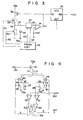
- the output terminal of the operational amplifier 31 is also coupled with the gate of a P channel MOS transistor 32.
- the transistor 32 operates in a saturation region and serves as a constant current source for generating a current dependent on the output voltage Vc.
- the source of the transistor 32 is coupled with a terminal or a point to which power voltage VDD is applied. This terminal will frequently be called a VDD supply.
- the drain of the transistor 32 is connected to one of the fixed contacts of a first switch 33.
- the other fixed contact of the switch 33 is connected to one of the fixed contacts of a second switch 34.
- the other fixed contact of the second switch 34 is coupled with a terminal or a point to which ground potential VSS is applied. This terminal will be frequently called a VSS supply.
- connection point of the drains of the transistors 42 and 43 is connected to one of the electrodes of a capacitor 47.
- the capacitor 47 is connected to the VSS supply.
- connection point between the drains of the transistors 44 and 45 is connected to one of the electrodes of a capacitor 49.
- the other electrode of the capacitor 49 is connected to the VSS supply.
- the one electrode of the capacitor 47, i.e., the node 46 is connected to the positive input terminal of a first comparator 50.
- the one electrode of the capacitor 49, i.e., the node 48 is connected to the positive input terminal of a second comparator 51.
- the input voltage Vin is applied to the negative input terminals of the comparators 50 and 51.
- the output signal of the first comparator 50 is connected to the set input terminal of a flip-flop (F F ) 54.
- the output terminal of the second comparator 51 is coupled with the reset input terminal of the FF 54.
- the Q and Q output signals each oscillate at a predetermined frequency.
- the Q output signal is used as the output signal of the oscillating section 30, as described above.
- the oscillating frequency of the output signal can be varied by changing the output voltage Vc of either the operational amplifier 31 or the input voltage Vin.
- the frequency f can be expressed by where C47 and C49 are capacitances of the capacitors 47 and 49.
- I4i is the current flowing through the transistor 41.
- TDO is a signal delay time of the first comparator 50.
- TD1 is a signal delay time of the second comparator 51.
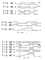
- the timing charts shown in Figs. 6A to 6C illustrate the operation of the VOC except the oscillating section 30.
- the timing control circuit 38 produces the first and second control signals Sl and S 2 at the timings shown in Figs. 6A and 6B. As shown, in the signal Sl, a logical "0" state continues for a period T0. In the signal S2, the logical "0" state still continues for a predetermined period of time after the signal Sl is pulsed to the high level or logical
- the capacitors 36, 37 and 39 have the same capacitance C, and the current ratio G is 1. Nonetheless, the present invention is not limited to this embodiment.
- the capacitors may have different capacitances, and the gate length and other structural features of each transistor may be changed..
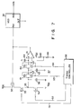
- Circuitry including the switches 33 and 34, the sample/hold circuit 37 and the reference voltage Vref, will be described referring to Fig. 7.
- the first switch 33 is constructed with a P channel MOS transistor. One end of the current path of this MOS transistor is connected to the P channel MOS transistor 32, and the other end to the second switch 34. The gate of the MOS transistor of the first switch 33 is connected for reception to the first control signal S l.
- the second switch 34 is constructed with an N channel MOS transistor. One end of this MOS transistor is connected to the first switch 33, while the other end is connected to the VSS supply. The gate of the MOS transistor receives the second control signal S2.
- the sample/hold circuit 37 is comprised of first and second CMOS analog switches 61 and 62, and capacitors 63 and 64.
- the first analog switch 61 is made up of P channel and N channel MOS transistors of which the current paths are connected in parallel. The node of the interconnection between one set of ends of the current paths of the paired transistors is connected to one of the electrodes of the capacitor 36.
- the third control signal S3 is supplied to the gate of the N channel MOS transistor in the analog switch 61.
- the control signal S3 is inverted by an inverter and supplied to the gate of the P channel MOS transistor of the same switch 61.
- the output terminal of the first analog switch 61 is connected to one of the electrodes of a capacitor 63.
- the capacitor 63 is earthed at the other electrode.
- the analog switch 62 has substantially the same circuit arrangement as that of the first analog switch 61, and is under the control of the fourth control signal S4.
- the input terminal of the analog switch 62 is coupled with the output terminal of the first analog switch 61 and the capacitor 63.
- a capacitor 64 is inserted between the output terminal of the second analog switch and ground.
- the node between the output terminal of the second analog switch 62 and the capacitor 64 serves as an output terminal of the sample/hold circuit 37.
- the capacitor 64 may be a stray capacitance present in association with the output terminal of the second switch 62 and the input terminal of the operational amplifier 31.
- the reference voltage Vref applied to the negative input terminal of the operational amplifier 31 is derived from a node between resistors 65 and 66, which are connected in series between the VDD supply and ground. Thus, the VDD voltage is divided according to the resistance ratio of these resistors. The divided voltage is used as the reference voltage Vref.
- the operation of the voltage controlled oscillator as illustrated in Fig. 7 will be described referring to Figs. 8A to 8F.
- the control signals Sl to S4 are formed using the clock pulses CLK shown in Fig. 8A.
- the trailing edge of the signal Sl (Fig. 8B) is delayed by a given period td behind the trailing edge of the signal S2. This indicates that the charge time of the capacitor 36 is (TO - td).
- the first switch 33 When the signal Sl is logical "0", the first switch 33 is turned on. At this time, the signal S2 is logical "0" and the second switch 34 is in an off state. Under this condition, the capacitor 36 is charged. The charged voltage of the capacitor 36 rises linearly.
- the signal Sl When the signal Sl is logical "1”, the first switch 33 is turned off to terminate the charging of the capacitor 36. Then, the signal S3 becomes logical "l”, so that the charged potential across the capacitor 36 is kept by the capacitor 63. Subsequently, the signal S4 becomes logical "1", and the voltage across the capacitor 63 is kept by the capacitor 64. After the signal S3 becomes "1” in logical level, the signal S2 is pulsed to logical "1" to allow the discharge of the capacitor 36.
- the signal S4 maintains logical "1" level during the period that the capacitor 36 is charged by the transistor 32, and discharged by the switch 34.
- the charged voltage across the capacitor 64 is applied, as the output voltage of the sample/hold circuit 37, to the positive input terminal of the operational amplifier 31.
- the purpose of providing the delay time td in the signal Sl is to compensate for the delay time TD in each of the comparators 50 and 51. If the delay time td is equal to the delay time TD, the charge time of the capacitor 36 is TO - TD. Therefore, in the equation (7), for example, the delay times TD and td are cancelled, remarkably reducing the effect by the delay time TD. Thus, even if the comparators 50 and 51 contain delay times, the VCO can produce an oscillating signal of an exact frequency.
- the clock pulses CLK are inverted and applied to the clock signal input of the latch 71.
- the Q output terminal of the latch 71 is coupled with the D input terminal of the latch 72.
- the Q output terminal of the latch 72 is coupled with the D input terminal of the latch 71.
- the clock input terminal of the latch 72 is coupled for reception with the clock pulses CLK.
- the Q bar output terminal of the FF 73 is connected to its D input terminal, and the Q output terminal thereof is coupled with the clock signal input terminal of an FF 74.
- the Q output terminal of the FF 74 is coupled with the D input terminal of the FF 74.
- the output signal of the latch 72 is frequency-divided into a factor of two by the FF 73 at the succeeding stage. Then, the output signal of the FF 73 is further frequency divided into a factor of two by the succeeding stage FF 74.
- the Q output terminal of the FF 74 is input to a delay circuit 80.
- the Q output signal of the FF 74 is input to the input terminal of a CMOS inverter 81 including a pair of P and N channel MOS transistors.
- One end of the current path of the P channel of the inverter 81 is connected to one end of the current path of a P channel MOS transistor 82.
- the other end of the current path of this transistor 82 is coupled with the VDD supply.
- the gate of the transistor 82 is coupled with the gate and one end of the current path of a P channel MOS transistor 83.
- the transistor 83 is connected at the other end of the current path to the VDD supply.
- the transistors 82 and 83 cooperate to form a current mirror circuit 84 which feeds a predetermined current to the P channel transistor of the inverter 81.
- the current path of an N channel MOS transistor 85 is inserted between the inverter 81 and a ground.
- the transistor 85 is biased to a fixed bias point by a bias source Vc.
- the transistor 85 feeds a fixed current to the N channel transistor of the inverter 81.
- the current path of an N channel MOS transistor 86 is inserted between the current mirror 84 and a ground.
- the same bias source Vc is applied to the gate of the transistor 86.
- the transistor 86 feeds a predetermined current to the current mirror 84.
- the output signal of the CMOS inverter 81 is input to an inverter 87.
- Both the output signal of the inverter 87 and the Q output signal of the FF 74 are applied to a NAND gate 88.
- the NAND gate 88 produces the first control signal Sl.
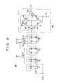
- a second embodiment of a voltage controlled oscillator according to the present invention will be described referring to Fig. 10.
- the output terminal of the sample/hold circuit 37 is connected to the negative input terminal of the operational amplifier 31.
- the positive input terminal of the operational amplifier 31 is coupled with the reference voltage Vref.
- a capacitor is connected between the negative input terminal and the output terminal of the operational amplifier 31.
- the amplifier 31 and the capacitor comprise an integration circuit.
- the output terminal is connected to the gate of an N channel MOS transistor 91.
- Another P channel MOS transistor 92 whose gate and one current path are connected to one end of the transistor 91 and the gates of the transistors 32 and 41.
- the other end of the current path of the transistor 92 is coupled with the VDD supply.
- the other end of the current path of the transistor 91 is grounded.
- the transistor 92 serves as a current load for the transistor 91.
- the transistors 32, 92 and 41 form a current mirror.
- FIG. 11 A detailed circuit arrangement which is available for the operational amplifier 31 and the comparators 50 and 51 in the oscillating section 30 (Fig. 4) will be described referring to Fig. 11.
- one end of the current path of an N channel M OS transistor 101 is connected to one end of that of an N channel MOS transistor 102.
- These transistors 102 and 103 constitute a differential amplifier 103.
- the other end of the transistor 101 is connected to one end of that of a P channel 104.
- the other end of the current path of this transistor is coupled with the VDD supply.
- the other end of the current path of the transistor 102 is connected to one end of the current path of a P channel MOS transistor 105. Its other end is coupled with the VDD supply.
- the gates of these transistors 104 and 105 are connected to the connection point between the current paths of the transistors 102 and 105.
- the transistors 104 and 105 form a current mirror circuit 106, which serves as a load for the differential pair 103.
- the connection point between the current paths of the transistors 101 and 102 is connected to one end of the current path of an N channel MOS transistor 107.
- the other end of the current path of this transistor is grounded.
- the transistor 107 serves as a current source to feed the operating current to the differential pair 103.
- a node between the transistors 101 and 104 is coupled with the gate of a P channel MOS transistor 108.
- the output signal of the differential pair 103 is supplied to the gate of the transistor 108.
- One end of the current path of the transistor 108 is connected to the VDD supply. Its other end is connected to one end of the current path of a N channel MOS transistor 109 as a current load for the transistor 108.
- the gate of the transistor 109 is connected to the gate of the transistor 107, and its other end is grounded.
- the gates of the transistors 107 and 109 are biased by a bias source 110.
- the gate of the transistor 101 is used as the positive input terminal, while the gate of the transistor 102 is used as the negative input terminal.
- the output signal is derived from a node between the transistors 108 and 109.
- FIG. 12 Another example of the operational amplifier will be given referring to Fig. 12.
- one end of the current path of an N channel MOS transistor 121 is connected to one end of that of an N channel M OS transistor 122. These transistors form a differential pair 123.
- a node between the transistors 121 and 122 is connected to one end of the current path of an N channel MOS transistor 124.
- the other end of the current path of this transistor 124 is grounded, and its gate is applied with a fixed voltage for biasing purposes.
- the other end of the current path of the transistor 121 is connected to the gate and one end of the current path of a P channel MOS transistor 125.
- the other end of the current path of the transistor 125 is coupled with the VDD supply.
- the other end of the current path of the transistor 122 is connected to the gate and one end of the current path of a P channel MOS transistor 126.
- the other end of the current path of this transistor 126 is coupled with the VDD supply.
- the transistors 128 and 125 are interconnected at the gates.
- the transistor 125 and 128 form a current mirror 127.
- the gate of the transistor 121 serves as an inverting input terminal, while that of the transistor 122 serves as a noninverting input terminal.
- the output signal is derived from a node between the transistors 130 and 132.
- the oscillating section 30 may employ many circuit other arrangements other than that of Fig. 4.
- One of such candidates is illustrated in Fig. 13.
- like reference numerals are used for indicating like or equivalent portions in Fig. 4.
- the two positive input terminals of a three-input comparator 140 are coupled for reception with the potential VA of the capacitor 47 and the potential VB of the capacitor 49.
- the input voltage Vin is applied to the negative input terminal of the comparator 140.
- the comparator 140 operates so as to compare the voltage Vin at the negative input terminal with either of the potentials at the positive input terminals for the purpose of determining which is higher than the other.
- the output signal of the comparator 140 is supplied through an inverter 141 to a select circuit 150.
- the select circuit 150 is comprised of two AND gates 151 and 152, and an inverter 153.
- the input terminals of the AND gates 151 and 152 receive the output signal of the inverter 141.
- the other input terminal of the AND gate 151 is coupled for reception with the Q signal of the FF 54 through a delay circuit 160 to be given later.
- the delayed Q signal of the FF 54 is applied through an inverter 153 to the other input terminal of the AND gate 152.
- the output terminal of the AND gate 151 is connected to the set input terminal of the FF 54.
- the output terminal of the AND gate 145 is connected to the reset input terminal of the FF 54.
- the Q output signal of the FF 54 is input to the delay circuit 160.
- the delay circuit 160 is comprised of an inverter 161 coupled for reception with the Q output signal of the FF 54, a capacitor 162 inserted between the output terminal of the inverter 161 and ground, another inverter 163 coupled for reception with the output signal of the inverter 161, and another capacitor 164 coupled between the output terminal of the inverter and ground.
- the output signal of the inverter 163 is applied, as a delayed signal, to the select circuit 150.
- the delayed signal and the Q signal are coupled for transmission with an exclusive OR gate 170.
- the output signal of the exclusive OR gate 170 is supplied to the gate of a P channel MOS transistor 171.
- the current path of this transistor 171 is placed between the output terminal of the comparator 140 and the VDD supply.
- the present embodiment forcibly places the output signal of the comparator 140 into logical "1" for the signal delay time and by the delay circuit 160. Then, the select circuit 150 is switched to another state. In this way, the undesired inversion of the FF 54 is prevented.
Landscapes
- Stabilization Of Oscillater, Synchronisation, Frequency Synthesizers (AREA)
Applications Claiming Priority (2)
| Application Number | Priority Date | Filing Date | Title |
|---|---|---|---|
| JP59229229A JPS61107810A (ja) | 1984-10-31 | 1984-10-31 | 電圧制御発振回路 |
| JP229229/84 | 1984-10-31 |
Publications (3)
| Publication Number | Publication Date |
|---|---|
| EP0180105A2 true EP0180105A2 (fr) | 1986-05-07 |
| EP0180105A3 EP0180105A3 (en) | 1988-04-06 |
| EP0180105B1 EP0180105B1 (fr) | 1991-12-18 |
Family
ID=16888853
Family Applications (1)
| Application Number | Title | Priority Date | Filing Date |
|---|---|---|---|
| EP85113189A Expired EP0180105B1 (fr) | 1984-10-31 | 1985-10-17 | Oscillateur commandé par tension |
Country Status (4)
| Country | Link |
|---|---|
| US (1) | US4623852A (fr) |
| EP (1) | EP0180105B1 (fr) |
| JP (1) | JPS61107810A (fr) |
| DE (1) | DE3584944D1 (fr) |
Cited By (1)
| Publication number | Priority date | Publication date | Assignee | Title |
|---|---|---|---|---|
| AU612297B2 (en) * | 1989-08-14 | 1991-07-04 | Delco Electronics Corporation | Voltage controlled oscillator |
Families Citing this family (28)
| Publication number | Priority date | Publication date | Assignee | Title |
|---|---|---|---|---|
| JPS62260420A (ja) * | 1986-04-28 | 1987-11-12 | シ−メンス、アクチエンゲゼルシヤフト | 集積nmos回路装置 |
| JPH021620A (ja) * | 1987-11-30 | 1990-01-05 | Toshiba Corp | 電圧制御発振回路 |
| US4972162A (en) * | 1988-02-16 | 1990-11-20 | At&T Bell Laboratories | Wideband relaxation oscillator utilizing parasitic capacitances |
| JP2531742B2 (ja) * | 1988-05-17 | 1996-09-04 | 株式会社東芝 | 電圧制御発振回路 |
| JP2635789B2 (ja) * | 1989-01-17 | 1997-07-30 | 株式会社東芝 | 信号遅延回路及び該回路を用いたクロック信号発生回路 |
| US5128634A (en) * | 1990-10-29 | 1992-07-07 | Motorola, Inc. | Oscillator cirucit independent or parasitic capacitors |
| GB2268647B (en) * | 1992-07-02 | 1996-04-10 | Motorola Inc | Voltage controlled oscillator |
| US5604466A (en) * | 1992-12-08 | 1997-02-18 | International Business Machines Corporation | On-chip voltage controlled oscillator |
| DE69614501T2 (de) * | 1996-03-08 | 2002-04-11 | Co.Ri.M.Me. Consorzio Per La Ricerca Sulla Microelettronica Nel Mezzogiorno, Catania | Integrierte Schaltung mit automatischer Kompensation der Sollwertabweichungen der Kapazitäten |
| DE10257536B4 (de) * | 2002-12-10 | 2011-07-07 | Newlogic Technologies Gmbh | Spannungsgesteuerter Oszillator |
| JP2005117140A (ja) * | 2003-10-03 | 2005-04-28 | Nec Electronics Corp | 発振回路及びそれを備える半導体集積回路 |
| US7116181B2 (en) * | 2004-12-21 | 2006-10-03 | Actel Corporation | Voltage- and temperature-compensated RC oscillator circuit |
| JP4899215B2 (ja) * | 2006-02-28 | 2012-03-21 | 学校法人東海大学 | 電圧制御発振器および電圧制御発振方法 |
| JP4829724B2 (ja) * | 2006-09-06 | 2011-12-07 | 川崎マイクロエレクトロニクス株式会社 | 発振回路 |
| US7733191B2 (en) * | 2007-02-28 | 2010-06-08 | Freescale Semiconductor, Inc. | Oscillator devices and methods thereof |
| JP4938815B2 (ja) * | 2008-08-19 | 2012-05-23 | 旭化成エレクトロニクス株式会社 | 電圧制御発振器およびその調整方法 |
| JP2010136001A (ja) * | 2008-12-03 | 2010-06-17 | Renesas Electronics Corp | 発振器 |
| JP2010226358A (ja) * | 2009-03-23 | 2010-10-07 | Asahi Kasei Electronics Co Ltd | 電圧制御発振器および電圧制御発振方法 |
| US8026770B2 (en) * | 2009-07-01 | 2011-09-27 | Synaptics, Inc. | Relaxation oscillator |
| US8242853B2 (en) * | 2010-02-02 | 2012-08-14 | Analog Devices, Inc. | Low headroom oscillator |
| JP5375753B2 (ja) * | 2010-06-17 | 2013-12-25 | ミツミ電機株式会社 | 発振回路及びその動作電流制御方法 |
| WO2012001846A1 (fr) | 2010-06-28 | 2012-01-05 | パナソニック株式会社 | Circuit générateur de fréquence de référence, circuit intégré à semiconducteur et appareil électronique |
| US8319567B1 (en) * | 2011-06-10 | 2012-11-27 | Analog Devices, Inc. | Two oscillator synchronization system |
| US9300302B2 (en) * | 2012-04-20 | 2016-03-29 | Freescale Semiconductor, Inc. | Oscillator circuit, a semiconductor device and an apparatus |
| CN103580655B (zh) * | 2012-07-24 | 2017-05-17 | 飞思卡尔半导体公司 | 比较器和采用比较器的张弛振荡器 |
| GB2533390A (en) * | 2014-12-19 | 2016-06-22 | Nordic Semiconductor Asa | Relaxation oscillator |
| US20170149385A1 (en) * | 2015-11-24 | 2017-05-25 | Infineon Technologies Ag | Fast starting crystal oscillator with low variation |
| US11444573B1 (en) * | 2021-09-17 | 2022-09-13 | KaiKuTek Inc. | Oscillator |
Family Cites Families (5)
| Publication number | Priority date | Publication date | Assignee | Title |
|---|---|---|---|---|
| US4110704A (en) | 1977-09-19 | 1978-08-29 | Motorola, Inc. | Astable multivibrator with temperature compensation and requiring a single supply voltage |
| US4131861A (en) * | 1977-12-30 | 1978-12-26 | International Business Machines Corporation | Variable frequency oscillator system including two matched oscillators controlled by a phase locked loop |
| US4374335A (en) * | 1980-05-19 | 1983-02-15 | Precision Monolithics, Inc. | Tuneable I.C. active integrator |
| FR2520953B1 (fr) * | 1982-01-29 | 1988-10-14 | Enertec | Convertisseur tension-frequence a haute stabilite |
| FR2528261B1 (fr) * | 1982-06-08 | 1987-12-11 | Thomson Csf | Generateur d'impulsions ayant une duree fixe proportionnelle a une duree de reference |
-
1984
- 1984-10-31 JP JP59229229A patent/JPS61107810A/ja active Pending
-
1985
- 1985-10-17 DE DE8585113189T patent/DE3584944D1/de not_active Expired - Lifetime
- 1985-10-17 EP EP85113189A patent/EP0180105B1/fr not_active Expired
- 1985-10-18 US US06/789,102 patent/US4623852A/en not_active Expired - Lifetime
Cited By (1)
| Publication number | Priority date | Publication date | Assignee | Title |
|---|---|---|---|---|
| AU612297B2 (en) * | 1989-08-14 | 1991-07-04 | Delco Electronics Corporation | Voltage controlled oscillator |
Also Published As
| Publication number | Publication date |
|---|---|
| EP0180105A3 (en) | 1988-04-06 |
| DE3584944D1 (de) | 1992-01-30 |
| EP0180105B1 (fr) | 1991-12-18 |
| JPS61107810A (ja) | 1986-05-26 |
| US4623852A (en) | 1986-11-18 |
Similar Documents
| Publication | Publication Date | Title |
|---|---|---|
| EP0180105B1 (fr) | Oscillateur commandé par tension | |
| US4623851A (en) | Voltage controlled oscillator using flip-flop controlled switching circuits | |
| US5552748A (en) | Digitally-tuned oscillator including a self-calibrating RC oscillator circuit | |
| US5644270A (en) | Enchanced stability voltage controlled RC oscillator | |
| US5594388A (en) | Self-calibrating RC oscillator | |
| US5646563A (en) | Charge pump with near zero offset current | |
| US5740213A (en) | Differential charge pump based phase locked loop or delay locked loop | |
| EP0574982B1 (fr) | Pompe de charge à capacité commutée ainsi qu' oscillateur en dents de scie comprenant une telle pompe de charge | |
| US6326859B1 (en) | Oscillator circuit having trimmable capacitor array receiving a reference current | |
| US6121805A (en) | Universal duty cycle adjustment circuit | |
| US6191660B1 (en) | Programmable oscillator scheme | |
| US5764110A (en) | Voltage controlled ring oscillator stabilized against supply voltage fluctuations | |
| KR960005193B1 (ko) | 발진 회로 | |
| US5663675A (en) | Multiple stage tracking filter using a self-calibrating RC oscillator circuit | |
| US6377129B1 (en) | Programmable relaxation oscillator | |
| EP0788236A1 (fr) | Synthétiseur de fréquence à PLL avec contrÔle de gain du circuit de pompe de charge | |
| EP0379169B1 (fr) | Circuit retardeur de signaux utilisant un circuit pompe de charge | |
| EP0318930B1 (fr) | Oscillateur commandé en tension | |
| EP0072751A2 (fr) | Circuit à boucle d'asservissement de phase | |
| US4785262A (en) | Pulse generator producing pulses having a width free from a power voltage and a threshold voltage of an inverter used therein | |
| US6753739B1 (en) | Programmable oscillator scheme | |
| US4786824A (en) | Input signal level detecting circuit | |
| US5585765A (en) | Low power RC oscillator using a low voltage bias circuit | |
| US5589802A (en) | Circuit for detecting the absence of an external component | |
| EP1109317A1 (fr) | Oscillateur de commande et procédé associé |
Legal Events
| Date | Code | Title | Description |
|---|---|---|---|
| PUAI | Public reference made under article 153(3) epc to a published international application that has entered the european phase |
Free format text: ORIGINAL CODE: 0009012 |
|
| 17P | Request for examination filed |
Effective date: 19851114 |
|
| AK | Designated contracting states |
Kind code of ref document: A2 Designated state(s): DE GB IT |
|
| PUAL | Search report despatched |
Free format text: ORIGINAL CODE: 0009013 |
|
| AK | Designated contracting states |
Kind code of ref document: A3 Designated state(s): DE GB IT |
|
| 17Q | First examination report despatched |
Effective date: 19900627 |
|
| GRAA | (expected) grant |
Free format text: ORIGINAL CODE: 0009210 |
|
| AK | Designated contracting states |
Kind code of ref document: B1 Designated state(s): DE GB IT |
|
| ITF | It: translation for a ep patent filed | ||
| REF | Corresponds to: |
Ref document number: 3584944 Country of ref document: DE Date of ref document: 19920130 |
|
| PLBE | No opposition filed within time limit |
Free format text: ORIGINAL CODE: 0009261 |
|
| STAA | Information on the status of an ep patent application or granted ep patent |
Free format text: STATUS: NO OPPOSITION FILED WITHIN TIME LIMIT |
|
| 26N | No opposition filed | ||
| PGFP | Annual fee paid to national office [announced via postgrant information from national office to epo] |
Ref country code: GB Payment date: 19971008 Year of fee payment: 13 |
|
| PGFP | Annual fee paid to national office [announced via postgrant information from national office to epo] |
Ref country code: DE Payment date: 19971024 Year of fee payment: 13 |
|
| PG25 | Lapsed in a contracting state [announced via postgrant information from national office to epo] |
Ref country code: GB Free format text: LAPSE BECAUSE OF NON-PAYMENT OF DUE FEES Effective date: 19981017 |
|
| GBPC | Gb: european patent ceased through non-payment of renewal fee |
Effective date: 19981017 |
|
| PG25 | Lapsed in a contracting state [announced via postgrant information from national office to epo] |
Ref country code: DE Free format text: LAPSE BECAUSE OF NON-PAYMENT OF DUE FEES Effective date: 19990803 |