EP0180183A2 - Plaquette de circuit imprimé multicouche - Google Patents
Plaquette de circuit imprimé multicouche Download PDFInfo
- Publication number
- EP0180183A2 EP0180183A2 EP85113697A EP85113697A EP0180183A2 EP 0180183 A2 EP0180183 A2 EP 0180183A2 EP 85113697 A EP85113697 A EP 85113697A EP 85113697 A EP85113697 A EP 85113697A EP 0180183 A2 EP0180183 A2 EP 0180183A2
- Authority
- EP
- European Patent Office
- Prior art keywords
- hole
- diameter
- wiring board
- printed wiring
- layers
- Prior art date
- Legal status (The legal status is an assumption and is not a legal conclusion. Google has not performed a legal analysis and makes no representation as to the accuracy of the status listed.)
- Ceased
Links
Images

Classifications
-
- H—ELECTRICITY
- H05—ELECTRIC TECHNIQUES NOT OTHERWISE PROVIDED FOR
- H05K—PRINTED CIRCUITS; CASINGS OR CONSTRUCTIONAL DETAILS OF ELECTRIC APPARATUS; MANUFACTURE OF ASSEMBLAGES OF ELECTRICAL COMPONENTS
- H05K1/00—Printed circuits
- H05K1/02—Details
- H05K1/11—Printed elements for providing electric connections to or between printed circuits
- H05K1/115—Via connections; Lands around holes or via connections
- H05K1/116—Lands, clearance holes or other lay-out details concerning the surrounding of a via
-
- H—ELECTRICITY
- H05—ELECTRIC TECHNIQUES NOT OTHERWISE PROVIDED FOR
- H05K—PRINTED CIRCUITS; CASINGS OR CONSTRUCTIONAL DETAILS OF ELECTRIC APPARATUS; MANUFACTURE OF ASSEMBLAGES OF ELECTRICAL COMPONENTS
- H05K1/00—Printed circuits
- H05K1/02—Details
- H05K1/0286—Programmable, customizable or modifiable circuits
- H05K1/0287—Programmable, customizable or modifiable circuits having an universal lay-out, e.g. pad or land grid patterns or mesh patterns
-
- H—ELECTRICITY
- H05—ELECTRIC TECHNIQUES NOT OTHERWISE PROVIDED FOR
- H05K—PRINTED CIRCUITS; CASINGS OR CONSTRUCTIONAL DETAILS OF ELECTRIC APPARATUS; MANUFACTURE OF ASSEMBLAGES OF ELECTRICAL COMPONENTS
- H05K1/00—Printed circuits
- H05K1/02—Details
- H05K1/0296—Conductive pattern lay-out details not covered by sub groups H05K1/02 - H05K1/0295
- H05K1/0298—Multilayer circuits
-
- H—ELECTRICITY
- H05—ELECTRIC TECHNIQUES NOT OTHERWISE PROVIDED FOR
- H05K—PRINTED CIRCUITS; CASINGS OR CONSTRUCTIONAL DETAILS OF ELECTRIC APPARATUS; MANUFACTURE OF ASSEMBLAGES OF ELECTRICAL COMPONENTS
- H05K2201/00—Indexing scheme relating to printed circuits covered by H05K1/00
- H05K2201/09—Shape and layout
- H05K2201/09209—Shape and layout details of conductors
- H05K2201/0929—Conductive planes
- H05K2201/09309—Core having two or more power planes; Capacitive laminate of two power planes
-
- H—ELECTRICITY
- H05—ELECTRIC TECHNIQUES NOT OTHERWISE PROVIDED FOR
- H05K—PRINTED CIRCUITS; CASINGS OR CONSTRUCTIONAL DETAILS OF ELECTRIC APPARATUS; MANUFACTURE OF ASSEMBLAGES OF ELECTRICAL COMPONENTS
- H05K2201/00—Indexing scheme relating to printed circuits covered by H05K1/00
- H05K2201/09—Shape and layout
- H05K2201/09209—Shape and layout details of conductors
- H05K2201/09372—Pads and lands
- H05K2201/09454—Inner lands, i.e. lands around via or plated through-hole in internal layer of multilayer PCB
-
- H—ELECTRICITY
- H05—ELECTRIC TECHNIQUES NOT OTHERWISE PROVIDED FOR
- H05K—PRINTED CIRCUITS; CASINGS OR CONSTRUCTIONAL DETAILS OF ELECTRIC APPARATUS; MANUFACTURE OF ASSEMBLAGES OF ELECTRICAL COMPONENTS
- H05K2201/00—Indexing scheme relating to printed circuits covered by H05K1/00
- H05K2201/09—Shape and layout
- H05K2201/09209—Shape and layout details of conductors
- H05K2201/095—Conductive through-holes or vias
- H05K2201/09609—Via grid, i.e. two-dimensional array of vias or holes in a single plane
-
- H—ELECTRICITY
- H05—ELECTRIC TECHNIQUES NOT OTHERWISE PROVIDED FOR
- H05K—PRINTED CIRCUITS; CASINGS OR CONSTRUCTIONAL DETAILS OF ELECTRIC APPARATUS; MANUFACTURE OF ASSEMBLAGES OF ELECTRICAL COMPONENTS
- H05K2201/00—Indexing scheme relating to printed circuits covered by H05K1/00
- H05K2201/09—Shape and layout
- H05K2201/09209—Shape and layout details of conductors
- H05K2201/09654—Shape and layout details of conductors covering at least two types of conductors provided for in H05K2201/09218 - H05K2201/095
- H05K2201/0969—Apertured conductors
-
- H—ELECTRICITY
- H05—ELECTRIC TECHNIQUES NOT OTHERWISE PROVIDED FOR
- H05K—PRINTED CIRCUITS; CASINGS OR CONSTRUCTIONAL DETAILS OF ELECTRIC APPARATUS; MANUFACTURE OF ASSEMBLAGES OF ELECTRICAL COMPONENTS
- H05K2201/00—Indexing scheme relating to printed circuits covered by H05K1/00
- H05K2201/09—Shape and layout
- H05K2201/09209—Shape and layout details of conductors
- H05K2201/09654—Shape and layout details of conductors covering at least two types of conductors provided for in H05K2201/09218 - H05K2201/095
- H05K2201/09718—Clearance holes
-
- H—ELECTRICITY
- H05—ELECTRIC TECHNIQUES NOT OTHERWISE PROVIDED FOR
- H05K—PRINTED CIRCUITS; CASINGS OR CONSTRUCTIONAL DETAILS OF ELECTRIC APPARATUS; MANUFACTURE OF ASSEMBLAGES OF ELECTRICAL COMPONENTS
- H05K2201/00—Indexing scheme relating to printed circuits covered by H05K1/00
- H05K2201/09—Shape and layout
- H05K2201/09818—Shape or layout details not covered by a single group of H05K2201/09009 - H05K2201/09809
- H05K2201/09945—Universal aspects, e.g. universal inner layers or via grid, or anisotropic interposer
-
- H—ELECTRICITY
- H05—ELECTRIC TECHNIQUES NOT OTHERWISE PROVIDED FOR
- H05K—PRINTED CIRCUITS; CASINGS OR CONSTRUCTIONAL DETAILS OF ELECTRIC APPARATUS; MANUFACTURE OF ASSEMBLAGES OF ELECTRICAL COMPONENTS
- H05K2201/00—Indexing scheme relating to printed circuits covered by H05K1/00
- H05K2201/10—Details of components or other objects attached to or integrated in a printed circuit board
- H05K2201/10613—Details of electrical connections of non-printed components, e.g. special leads
- H05K2201/10621—Components characterised by their electrical contacts
- H05K2201/10689—Leaded Integrated Circuit [IC] package, e.g. dual-in-line [DIL]
-
- H—ELECTRICITY
- H05—ELECTRIC TECHNIQUES NOT OTHERWISE PROVIDED FOR
- H05K—PRINTED CIRCUITS; CASINGS OR CONSTRUCTIONAL DETAILS OF ELECTRIC APPARATUS; MANUFACTURE OF ASSEMBLAGES OF ELECTRICAL COMPONENTS
- H05K3/00—Apparatus or processes for manufacturing printed circuits
- H05K3/40—Forming printed elements for providing electric connections to or between printed circuits
- H05K3/42—Plated through-holes or plated via connections
- H05K3/429—Plated through-holes specially for multilayer circuits, e.g. having connections to inner circuit layers
Definitions
- the present invention relates to a multilayer printed wiring board (abbreviated PWB hereinafter) and especially to an improvement in the interlayer connection.
- PWB multilayer printed wiring board
- FIG. 1 shows a composition of layers of four-layer PWB which is generally used
- Fig. 2 shows a cross sectional view of the PWB composed of above-mentioned layers along the center of a plated through hole.
- the surface layer defines the first layer (Ll), the bottom layer defines the fourth layer (L4) and two internal layers define the second (L2) and third (L3) layers, and the second layer is usually used as a ground plane, the third layer is used as a power supply plane, and the first and fourth layers are used as the signal line planes on which the circuit components are mounted and wirings are formed.
- the above-mentioned multilayer PWB is manufactured as follows:
- Fig. 1 and Fig. 2 show the structure of two plated through holes 10A and 10B.
- Ll plane has lands l A and 1B around the respective through holes l0A and 10B, which have signal lines 2A and 2B respectively.
- L2 plane has copper foil on the whole surface except the round clearance holes (or reverse land) 4 around the through hole walls 11A and 11B.
- L3 plane also has clearance hole 7 around the through hole wall llB and has copper foil around the through hole llA.
- the functional land is composed of an annular clearance hole 6A, i.e. a part which is not provided with copper foil, a land connected to the through hole wall 11A and bridging parts.
- L4 the bottom layer, has land 8A without signal lines at through hole 10A, and has land 8B with a signal line 9 at through hole 10B.
- L3 plane is connected to the Ll plane and L4 plane by the through hole wall 11A.
- Fig. 3 is an enlarged view of the same internal layer pattern 100 as used at the through hole 10A, and it shows the condition before drilling.
- the functional land is composed of annular copperless reverse land 102 which has a predetermined width, a land 104 within the reverse land 102 and bridging sections formed every 90° and connecting the land 104 to the copper foil area.
- the method in which the internal connection or non-connection is selected according to the requirement of through hole involves the restriction on pattern design. That is, as described above, internal layers which are used as a power supply plane and a ground plane are fundamentally of the whole copper foil pattern and may well be common to every kind of printed wiring board. However, conventional internal layer pattern must be changed according to the kind of PWB and, on the contrary, if the internal layer pattern is determined, the functions of lands on the surface layer or bottom layer are determined and unchangeable. Consequently, outer layer pattern design is restricted and the wiring density may be decreased.
- Fig. 4 explains the state after the ICs are mounted to the conventional multilayer PWB.
- Fig. 4(a) shows the mounting of a 14-pin IC 20
- Fig. 4(b) shows the mounting of a 20-pin IC 30.
- the ground pin 21 must be connected to the ground line
- the power supply pin 22 must be connected to the power supply line.
- through hole 41 shown by mark +
- the through hole 42 shown by mark X
- the ground pin 31 must be connected to the through hole 41 and the power supply pin 32 must be connected to the through hole 42 using the connection lines 45 and 46.
- each through hole position is determined by the internal layer pattern which is commonly formed. Consequently the degree of freedom for mounting circuit components and wiring efficiency of surface plane and bottom plane may be decreased because the complex wiring patterns must be formed according to the component mounting status.
- this invention comprises three or more wiring layers having wiring patterns, through holes connecting an internal layer to at least one of different layers, at least one layer having interlayer connection patterns at basic grids, each of the interlayer connection patterns having a clearance when a small diameter through hole is formed, and having a land part contacted to the through hole when a large diameter through hole is formed, and the through holes being of a large diameter at the grids where interlayer connections are performed, and other through hole being of a small diameter at the grids where interlayer connections are not performed.
- Fig. 5 illustrates the composition of layers of the present invention
- Fig. 6 illustrates the cross sectional view of the through-hole along the center thereof, and these correspond to Fig. 1 and Fig. 2, respectively.
- the diameter of a through hole 60A at part A is larger than the diameter of a through hole 60B at part B. That is, typically the drilling of the diameter of 1 mm at part A and the drilling of the diameter of 0.5 mm at part B are performed.
- the connection status at part A differs from that of part B.
- internal layer connection is accomplished because the diameter of the through hole 60A is larger than the diameter of the clearance hole pattern 204 which is for example 0.75 mm and the through hole wall 61A contacts the land 63.
- there is no internal connection because the diameter of the through hole 60B is smaller than the diameter of the clearance hole 62 and the through hole wall 61B exists within the clearance hole 62.
- Fig. 6 clearly shows the condition of interlayer connection, that is, the wall 61A of the large diameter through hole 60A contacts the land 63A and copper foil pattern 55 and the wall 61B of the small diameter through hole 60B is apart from the land 63B connected to copper foil pattern 55 with a clearance 62.
- the widths of lands on the surface layers Ll and L4 differ according to the through hole diameter, and the clearance between the through hole and the clearance hole varies, however this variation does not affect the performance of PWB adversely.
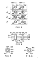
- FIG. 7 and Fig. 8 show the enlarged functional land pattern which operates as an interlayer connection at through hole part.
- a pattern 200 in the Fig. 7 has a circular clearance hole 204 and concentric annular clearance pattern 202 which is separated by bridge sections 203 at every approx. 90°, the bridge sections 203 connecting the copper foil around the clearnace hole 204 to the copper foil formed on whole surface around the clearance pattern 202.
- Clearance pattern 202 of the functional land is provided for preventing the heat diffusion from the through hole walls to the copper foil which has a large heat capacity.
- a pattern 300 shown in Fig. 8 provides a clearance pattern 304 which has four projections 302 formed at approx. every 90° in the copper foil 301.
- a circle 305 which is formed by the root part 303 has a diameter larger than the small through hole diameter and smaller than the large through hole.
- connection or non-connection can be selected by varying the diameter of the through hole. Therefore a common pattern having the above through hole pattern can be used commonly for many kinds of PWBs and the pattern on the surface layer is not restricted by the inner layer pattern and can be laid out, thus improving the wiring efficiency.
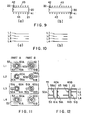
- Fig. 9 shows the wiring on the surface layer of the PWB of the present invention on which a component is mounted.
- Fig. 9(a) illustrates the mounting of 14- pin IC 20
- Fig. 9(b) illustrates the mounting of 20-pin IC 30.
- the side where the power supply pin is arranged and the side where the ground pin is arranged are determined. Therefore if for series of through holes located upper side of IC in Fig. 9, the interlayer connection pattern 200 shown in Fig. 7 is used as L2 plane as shown in Fig. 10(a), and for series of through holes located lower side of IC in Fig. 9, the interlayer connection pattern 200 shown in Fig. 7 is used as L3 plane as shown in Fig.
- interlayer connection patterns two kinds are described, however they are not limitative and any pattern which has parts contacting a large diameter through hole and separating from small diameter through hole, are applicable.
- Fig. 10 and Fig. 11 show another embodiment of this invention, and Fig. 10 shows the composition of laminates and Fig. 11 shows the cross sectional view along the center of the through holes.
- Ll of Fig. 5 is used as L3
- L2 of Fig. 5 is used as L4
- L3 of Fig. 5 is used as Ll
- L4 of Fig. 5 is used as L2.
- Such multilayer PWB is suitable for measuring instruments because of excellent anti-noise characteristics caused by the signal layers being sandwiched by copper foil layers.
- an arrangement may be in the form in which the patterns shown in Fig. 7 and Fig. 8 are provided at all grid locations.
- the above common interlayer connection patterns and clearance holes patterns may be provided alternately.
- this alternating pattern is used complementally, that is, at one grid, one internal layer is provided with the interlayer connectior pattern and the other internal layer is provided with the clearance hole pattern, connection and non-connection can be easily selected by varying the diameter of the through hole.
- internal layers can be designed commonly to various kinds of multilayer PWBs.
- Outer layers can be laid out without being affected by inner layers, so that the wiring efficiency and mounting density can be raised thoroughly. Therefore high density PWB can be obtained without increasing the number of layers and the size. Furthermore, manufacturing cost can be decreased because designing manhour and manufacturing time will be decreased.
Landscapes
- Engineering & Computer Science (AREA)
- Microelectronics & Electronic Packaging (AREA)
- Production Of Multi-Layered Print Wiring Board (AREA)
- Structure Of Printed Boards (AREA)
Applications Claiming Priority (4)
| Application Number | Priority Date | Filing Date | Title |
|---|---|---|---|
| JP22735184A JPS61104694A (ja) | 1984-10-29 | 1984-10-29 | 多層プリント基板の層間接続方法 |
| JP227351/84 | 1984-10-29 | ||
| JP27596584A JPS61156898A (ja) | 1984-12-28 | 1984-12-28 | 多層印刷配線板 |
| JP275965/84 | 1984-12-28 |
Publications (2)
| Publication Number | Publication Date |
|---|---|
| EP0180183A2 true EP0180183A2 (fr) | 1986-05-07 |
| EP0180183A3 EP0180183A3 (fr) | 1987-09-23 |
Family
ID=26527628
Family Applications (1)
| Application Number | Title | Priority Date | Filing Date |
|---|---|---|---|
| EP85113697A Ceased EP0180183A3 (fr) | 1984-10-29 | 1985-10-28 | Plaquette de circuit imprimé multicouche |
Country Status (2)
| Country | Link |
|---|---|
| EP (1) | EP0180183A3 (fr) |
| KR (1) | KR860003750A (fr) |
Cited By (8)
| Publication number | Priority date | Publication date | Assignee | Title |
|---|---|---|---|---|
| EP0481271A1 (fr) * | 1990-10-01 | 1992-04-22 | Sony Corporation | Plaquette à circuit imprimé multicouche et son procédé de fabrication |
| EP0621747A3 (fr) * | 1993-04-22 | 1995-03-08 | Ibm | Conception de masse thermique de panneaux ou cartes à circuit imprimé. |
| GB2374984A (en) * | 2001-04-25 | 2002-10-30 | Ibm | A circuitised substrate for high-frequency applications |
| EP1816905A2 (fr) | 1997-02-03 | 2007-08-08 | Ibiden Co., Ltd. | Plaquette à circuit imprimé et procédé de fabrication correspondant |
| CN103260339A (zh) * | 2012-02-21 | 2013-08-21 | 富士通株式会社 | 多层布线板和电子装置 |
| CN104519660A (zh) * | 2013-10-04 | 2015-04-15 | 特拉博斯股份有限公司 | 电路板 |
| CN107548229A (zh) * | 2016-06-27 | 2018-01-05 | 中兴通讯股份有限公司 | Pcb及其制造方法 |
| CN116665983A (zh) * | 2022-02-17 | 2023-08-29 | 纬创资通股份有限公司 | 带线结构、带线结构制作方法及其电子装置 |
Family Cites Families (2)
| Publication number | Priority date | Publication date | Assignee | Title |
|---|---|---|---|---|
| US3344515A (en) * | 1961-04-21 | 1967-10-03 | Litton Systems Inc | Multilayer laminated wiring |
| US3243498A (en) * | 1964-12-24 | 1966-03-29 | Ibm | Method for making circuit connections to internal layers of a multilayer circuit card and circuit card produced thereby |
-
1985
- 1985-10-28 EP EP85113697A patent/EP0180183A3/fr not_active Ceased
- 1985-10-29 KR KR1019850008009A patent/KR860003750A/ko not_active Abandoned
Cited By (14)
| Publication number | Priority date | Publication date | Assignee | Title |
|---|---|---|---|---|
| EP0481271A1 (fr) * | 1990-10-01 | 1992-04-22 | Sony Corporation | Plaquette à circuit imprimé multicouche et son procédé de fabrication |
| EP0621747A3 (fr) * | 1993-04-22 | 1995-03-08 | Ibm | Conception de masse thermique de panneaux ou cartes à circuit imprimé. |
| EP1816905A2 (fr) | 1997-02-03 | 2007-08-08 | Ibiden Co., Ltd. | Plaquette à circuit imprimé et procédé de fabrication correspondant |
| US7552531B2 (en) | 1997-02-03 | 2009-06-30 | Ibiden Co., Ltd. | Method of manufacturing a printed wiring board having a previously formed opening hole in an innerlayer conductor circuit |
| EP1816905A3 (fr) * | 1997-02-03 | 2007-10-03 | Ibiden Co., Ltd. | Plaquette à circuit imprimé et procédé de fabrication correspondant |
| US6710258B2 (en) | 2001-04-25 | 2004-03-23 | International Business Machines Corporation | Circuitized substrate for high-frequency applications |
| GB2374984B (en) * | 2001-04-25 | 2004-10-06 | Ibm | A circuitised substrate for high-frequency applications |
| GB2374984A (en) * | 2001-04-25 | 2002-10-30 | Ibm | A circuitised substrate for high-frequency applications |
| CN103260339A (zh) * | 2012-02-21 | 2013-08-21 | 富士通株式会社 | 多层布线板和电子装置 |
| CN104519660A (zh) * | 2013-10-04 | 2015-04-15 | 特拉博斯股份有限公司 | 电路板 |
| CN104519660B (zh) * | 2013-10-04 | 2018-07-03 | 特拉博斯股份有限公司 | 电路板 |
| CN107548229A (zh) * | 2016-06-27 | 2018-01-05 | 中兴通讯股份有限公司 | Pcb及其制造方法 |
| CN107548229B (zh) * | 2016-06-27 | 2022-01-28 | 中兴通讯股份有限公司 | Pcb及其制造方法 |
| CN116665983A (zh) * | 2022-02-17 | 2023-08-29 | 纬创资通股份有限公司 | 带线结构、带线结构制作方法及其电子装置 |
Also Published As
| Publication number | Publication date |
|---|---|
| EP0180183A3 (fr) | 1987-09-23 |
| KR860003750A (ko) | 1986-05-28 |
Similar Documents
| Publication | Publication Date | Title |
|---|---|---|
| US4799128A (en) | Multilayer printed circuit board with domain partitioning | |
| US5038252A (en) | Printed circuit boards with improved electrical current control | |
| US4543715A (en) | Method of forming vertical traces on printed circuit board | |
| EP0883330B1 (fr) | Plaquette à circuits imprimés avec trous traversants primaires et secondaires | |
| US4249302A (en) | Multilayer printed circuit board | |
| CA2422677C (fr) | Technique de reduction du nombre de couches d'une carte de circuits multicouche | |
| CA1137646A (fr) | Support de pastilles vlsi avec feuilles d'alimentation etagees a grande capacite inserees dans des fentes pratiquees dans le substrat | |
| US4524240A (en) | Universal circuit prototyping board | |
| US4772864A (en) | Multilayer circuit prototyping board | |
| US5856636A (en) | Electronic circuit prototype wiring board with visually distinctive contact pads | |
| US4016463A (en) | High density multilayer printed circuit card assembly and method | |
| WO2002001928A1 (fr) | Carte a circuit imprime sans traversees | |
| JPH07272932A (ja) | プリントインダクタ | |
| US5608192A (en) | Multilayer thin-film wiring board | |
| US20240357730A1 (en) | Printed circuit board and method of producing thereof | |
| JP2503725B2 (ja) | 多層配線基板 | |
| EP0166762A1 (fr) | Circuiterie électrique | |
| US4361634A (en) | Artwork master for production of multilayer circuit board | |
| EP0268111A2 (fr) | Procédé pour effectuer une modification technique des interconnexions entre plusieurs circuits intégrés en utilisant des pièces intermédiaires | |
| CN119893886A (zh) | 一种电路板上导电孔的成型方法及电路板 | |
| CA1055164A (fr) | Plaquette de circuits multicouche | |
| CA1260625A (fr) | Carte de circuits imprimes multicouche a partitionnement en domaines | |
| US20030102159A1 (en) | Optimum power and ground bump pad and bump patterns for flip chip packaging | |
| CN101808479B (zh) | 减少信号布线设备中的层数的方法 | |
| JPS5987896A (ja) | 多層プリント基板 |
Legal Events
| Date | Code | Title | Description |
|---|---|---|---|
| PUAI | Public reference made under article 153(3) epc to a published international application that has entered the european phase |
Free format text: ORIGINAL CODE: 0009012 |
|
| 17P | Request for examination filed |
Effective date: 19851127 |
|
| AK | Designated contracting states |
Kind code of ref document: A2 Designated state(s): DE GB IT NL |
|
| PUAL | Search report despatched |
Free format text: ORIGINAL CODE: 0009013 |
|
| AK | Designated contracting states |
Kind code of ref document: A3 Designated state(s): DE GB IT NL |
|
| 17Q | First examination report despatched |
Effective date: 19890414 |
|
| STAA | Information on the status of an ep patent application or granted ep patent |
Free format text: STATUS: THE APPLICATION HAS BEEN REFUSED |
|
| 18R | Application refused |
Effective date: 19900317 |
|
| RIN1 | Information on inventor provided before grant (corrected) |
Inventor name: HIRAOKA, MASARU Inventor name: IGARASHI, YUTAKA |