EP0180342A2 - Signalvergleichsschaltung und eine solche Schaltung verwendende Phasenregelschleife - Google Patents
Signalvergleichsschaltung und eine solche Schaltung verwendende Phasenregelschleife Download PDFInfo
- Publication number
- EP0180342A2 EP0180342A2 EP85307068A EP85307068A EP0180342A2 EP 0180342 A2 EP0180342 A2 EP 0180342A2 EP 85307068 A EP85307068 A EP 85307068A EP 85307068 A EP85307068 A EP 85307068A EP 0180342 A2 EP0180342 A2 EP 0180342A2
- Authority
- EP
- European Patent Office
- Prior art keywords
- signal
- output
- input
- producing
- frequency
- Prior art date
- Legal status (The legal status is an assumption and is not a legal conclusion. Google has not performed a legal analysis and makes no representation as to the accuracy of the status listed.)
- Withdrawn
Links
Images
Classifications
-
- H—ELECTRICITY
- H03—ELECTRONIC CIRCUITRY
- H03D—DEMODULATION OR TRANSFERENCE OF MODULATION FROM ONE CARRIER TO ANOTHER
- H03D13/00—Circuits for comparing the phase or frequency of two mutually-independent oscillations
- H03D13/003—Circuits for comparing the phase or frequency of two mutually-independent oscillations in which both oscillations are converted by logic means into pulses which are applied to filtering or integrating means
- H03D13/004—Circuits for comparing the phase or frequency of two mutually-independent oscillations in which both oscillations are converted by logic means into pulses which are applied to filtering or integrating means the logic means delivering pulses at more than one terminal, e.g. up and down pulses
Definitions
- the present invention relates to logic gate arrays of the type implemented by, for example, CMOS, NMOS and bipolar technologies. More particularly, the invention relates to a circuit for comparing the frequencies of two signals, such as a reference signal and an output signal. The invention also relates to a phase-locked-loop having a comparison circuit implementable as a gate array for comparing a reference signal to a signal representative of the output of a voltage controlled oscillator
- CMOS complementary metal-oxide-semiconductor
- NMOS complementary metal-oxide-semiconductor
- bipolar complementary metal-oxide-semiconductor
- the cells making up the individual gates of such a gate array are basically identical. It is only the interconnections between the various gates which differentiate one digital logic circuit from another. The circuit designer provides a desired circuitry implementation, merely by controlling the Interconnects between the various gate cells.
- the use of gate arrays simplifies and accelerates the manufacturing process.
- phase-locked-loop circuits used to assure a desired phase and frequency of a signal, rely for operation on comparison of an output signal of a voltage control oscillator with a reference signal. The phase and frequency of the output signal is then adjusted to conform to the phase and frequency of the reference signal.
- phase comparator (sometimes referred to as a phase "detector").
- a phase comparator is used to compare the requisite reference signal to the output of the voltage controlled oscillator.
- Such a comparator typically has one of two configurations: (a) "type-I” phase comparator, and a "type-II” phase comparator.
- a type-I phase comparator is an exclusive-OR network which operates in a manner analogous to an over-driven analog balanced mixer.
- a type-II phase comparator is an edge-controlled, digital memory network typically comprising four flip-flop stages, control gating and a three-state output circuit. Such a phase comparator reacts only to the edges of a reference signal and a signal representative of an error, so that the duty cycles of the signals are irrelevant.
- Type-II phase comparators for phase-locked- loops have been designed for custom monolithic circuitry. For example, a typical one may be found in the CMOS Integrated Circuit Manual (1980) published by RCA, pages 714-717 ("The RCA CMOS/MOS Phase-Locked-Loop: A Versatile Building Block for Micro-Power Digital and Analog Applications").
- phase comparators are not appropriately implementable in gate arrays. Due to unexpected circuit response caused by propagation and triggering delays, some of the components of phase comparators implemented by gate arrays may have outputs which conflict with the outputs of other phase comparator components.
- the result can be a logic decision error, causing the phase comparator to generate a large, incorrect error signal for one or more periods of the signals whose frequency and phase are being compared.
- the stability and response time of the phase-locked-loop suffers as a result of such operational errors of the phase comparator.
- phase-locked-loop is first powered on, it is possible that two mutually-exclusive internal control signals could be produced simultaneously. For instance, it is possible for the Q and 0 of a flip-flop to go high simultaneously, thus placing the flip-flop in an indeterminate state. Generally, extra logic is required to ensure that either this indeterminate state never can occur, or that the flip-flop can be reset out of this state if it does occur.
- One aspect of the present invention is a circuit implementable by a logic gate array structure for comparing the phase and frequency of a first periodic input signal with the phase and frequency of a second periodic input signal. It utilizes a master-slave relationship to substantially obviate the problems which may be caused by propagation and triggering delays in a gate array structure.
- a master indication device responsive to the first and second periodic input signals indicates which of the input signals last passed through a predetermined angular position.
- a slave indication device responsive to the indication of the master indication device and to the first and second input signals, indicates if one of the first and second input signals twice passed through the predetermined angular position since the other one of the first and second input signals passed through the predetermined angular position, thus indicating if one of the input signals is higher in frequency than the other.
- An output decoder is provided responsive to the indications of the master and slave indication devices to produce a signal if either of the first and second input signals both twice passes through the predetermined angular position since the other one of the signals does so and is also the last one of such signals to pass through the predetermined angular position (i.e., if one of the signals both is of a higher frequency than the other signal and leads the other signal in phase).
- the second indication device preferably is responsive to the first and second input signals after such signals have been delayed by predetermined time intervals.
- the major functions provided by the master indication device most simply are provided by a memory device such as a NAND latch, while the slave indication device preferably includes a NOR latch as a memory device.
- the master indication device also preferably includes a first master flip-flop which produces a pulse in response to the first input signal except when a first control signal is present, and a second master flip-flop which produces a pulse in response to the second input signal except when a second control signal is present.
- the NAND latch is responsive to the outputs of the first and second master flip-flops, and provides the first control signal when the first master flip-flop produces a pulse and the second control signal when the second master flip-flop produces a pulse.
- the NAND latch thus indicates which of the two input signals leads the other in phase.
- the slave indication device includes a first slave flip-flop which assumes a predetermined state in response to the simultaneous occurrence of a pulse produced by the first master flip-flop and the delayed first input signal, and a second slave flip-flop which assumes a predetermined state in response to the simultaneous occurrence of a pulse produced by the second master flip-flop and the delayed second input signal.
- the NOR latch then is responsive to the outputs of the first and second slave flip-flops, and indicates which of the first and second slave flip-flops last assumed their respective predetermined states. In this way it indicates which of the two input signals has a higher frequency than the other.
- the output decoder preferably is designed to be responsive to the states of the NAND and NOR latches to produce a first voltage level when the NAND and NOR latches are both in a first state, and to produce a second voltage level higher than the first voltage level when the NAND and NOR latches are both in a second state.
- the circuit of the invention is particularly useful in a phase-locked-loop circuit, responsive to the output signal of a voltage controlled oscillator and a reference signal, for producing a control voltage for such a circuit, the amplitude of which is determined by the difference between the phase or frequency of the output signal and the phase or frequency of the reference signal.
- the control voltage is used in such an arrangement to control the frequency of the voltage-controlled oscillator of the phase-locked-loop.
- a comparison circuit is provided by the invention that is highly stable and can operate at very high speeds.
- Such circuit may be implemented by gate array arrangements produced with CMOS technology - it has very low power consumption, is relatively inexpensive to fabricate, and is insensitive to fabrication variations. It is particularly useful to provide the comparison required by phase-locked-loop circuitry, using gate arrays. It does not introduce errors when the two inputs to be compared are at or near coincidence, and yet still provides very high speed operating capability. Indeed, the operating speed of the circuit is limited only by the propagation and delay times of the devices used. Moreover, each input is totally independent of the other input, so that the circuit is independent of inter-input timing. Yet, the design is such that it may be implemented by a simplified circuit which minimizes errors due to device variables and/or layout without sacrificing operating speed. Additionally, circuit latch-up upon power-up is avoided, thus preventing large output errors from occurring when the circuit is first turned on.
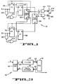
- Circuitry 12 compares the frequency and phase of a first signal A, which may be the reference signal of the phase-locked-loop circuit to be described, with the frequency and phase of a second input signal B and produces an output voltage at an output terminal 24 if the frequency or phase of signal A is different from the frequency or phase of signal B. In particular, circuit 12 determines which of signals A and B have the highest frequency and further detects any phase difference between the two inputs.
- a first signal A which may be the reference signal of the phase-locked-loop circuit to be described
- the frequency of signal A is higher than the frequency of signal B, or if its phase leads that of signal B, then it is desirable to apply a positive voltage to output terminal 24 (for instance, so as to raise the output frequency of a voltage controlled oscillator (VCO) of a phase-locked-looped circuit).
- VCO voltage controlled oscillator
- the frequency of signal A is less than the frequency of signal B, or if its phase lags that of signal B, it is desirable to apply a zero or negative voltage to output terminal 24 (for instance, in order to lower the frequency of a VCO). If the frequencies and phases of signals A and B are the same, it is desirable that output terminal 24 appear as an open circuit.
- the preferred embodiment of the circuit is sensitive only to the positive edges of signals A and B, thereby making the circuit immune to input duty cycle. To detect which of signals A and B have the highest frequency (if the frequencies of signals A and B are not the same), the preferred embodiment determines whether or not two or more positive edges of one of the signals occurs between two positive edges of the other signal.
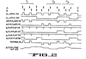
- FIG. 2 shows that during time period T 21 signal A has a higher frequency than signal B.
- the preferred embodiment of the comparison circuit 12 principally comprises in accordance with the present invention a master indication means, a slave indication means, and an output decoding means.
- the master indication means (which, in the preferred embodiment, comprises a NAND latch 32) is provided for determining which of the A and B signals last produced a leading edge (it will be understood that any arbitrary predetermined angular position such as the falling edge, the zero crossing point, a maximum or minimum point, etc., could be used instead of the leading edge). This indicates which of the two signals leads the other in phase.
- the slave indication means (which in the preferred embodiment comprises a NOR latch 38) is provided for determining if one of the signals A or B twice produced a leading-edge since the other one of the signals produced a leading edge.
- Output decoding means (which in the preferred embodiment comprises a NAND gate 40, a NOR gate 42, a p-MOSFET 44 and n-MOSFET 46) are provided for applying appropriate voltages to terminal 24 if predetermined conditions exist, as mentioned previously and to be discussed in greater detail below.
- delay means are provided for delaying the A and B signals by predetermined time intervals.
- first delay means which in the preferred embodiment comprise NAND gates 48 and 50, are provided for delaying the A signal by a predetermined time interval
- second delay means (which comprise NAND gates 52 and 54 in the preferred embodiment) are provided for delaying the B signal a predetermined time interval.
- Flip-flops 34 and 36 are responsive to the delayed signals A and B in order to permit them to function as slaves to flip-flops 28 and 30, respectively, as will be explained below.
- NAND latch 32 If NAND latch 32 is initially reset, a logic level zero will be applied to the D input of flip-flop 28.
- flip-flop 28 will normally be set, i.e., the Q output of the flip-flop will be at logic level 1.
- flip-flop 28 becomes reset, i.e., the Q output of the flip-flop goes to logic level 0, the value of the D input of the flip-flop at the time that a leading edge is applied to the flip-flop clock input.
- the Q output of flip-flop 28 is connected to the 9 input of NAND latch 32.
- the truth table for NAND latch 32 is as follows: As will be understood, when the logic level 0 output of flip-flop 28 occurs, NAND latch 32 will set, i.e., its Q output will go to logic level 1 and its will go to logic level 0. Q output of NAND latch 32 is connected back to the D input of flip-flop 28, and also to the asynchronous set ("present") input of the flip-flop. When the Q output of NAND latch 32 goes to logic level 1, flip-flop 28 will asynchronously set, i.e., its Q output will return to logic level 1.
- flip-flop 28 will normally be set; upon the occurrence of a leading edge of signal A, flip-flop 28 will produce a logic level 0 on its Q output for a short time, i.e., until NAND latch sets and asynchronously sets the flip-flop.
- Flip-flop 30 is connected to input signal B in the same manner that flip-flop 28 is connected to input signal A, and functions in precisely the same manner.
- the Q output of flip-flop 30 is connected to R input of NAND latch 32, while the D and S inputs of the flip-flop are connected to the Q output of the NAND latch. It will be understood that NAND latch 32 sets upon each leading edge of the input signal A, while the NAND latch resets upon each leading edge of input signal B. NAND latch 32 will therefore always indicate which input signal, A or B, produced the last leading edge, as can clearly be seen in the period T 1 of FIG. 2.
- NAND latch 32 When the first leading edge of input signal A occurs, flip-flop 28 generates a negative pulse (i.e., logic level 0) which sets NAND latch 32 (which, in turn sets flip-flop 28). If another leading edge of input signal A occurs before the next leading edge of input signal B, the Q output of flip-flop 28 will not assume the value appearing on the D input of the flip-flop because a logic level 1 appears on the D input of flip-flop 28.
- a negative pulse therefore will not be generated by the flip-flop (the Q output of the flip-flop is already at logic level 1).
- flip-flop 28 will only produce a negative pulse for the first leading edge of input signal A occurring after a leading edge of input signal B;
- flip-flop 30 will only produce a negative pulse for the first leading edge of input signal B occurring after a leading edge of input signal A.
- the Q output of flip-flop 28 is connected to the D input of flip-flop 34 (as well as to the 9 input of NAND latch 32).
- Input signal A is connected to a means for delaying the input signal by a predetermined time, which in turn is connected to the clock input of flip-flop 34.
- the means for delaying input signal A comprises a NAND gate 48 connected in series with a NAND gate 50, it will be understood by those skilled in the art that many different circuit configurations introducing a finite, predetermined time delay could be used instead, and that the number and nature of the components used to introduce the delay can be selected so as to determine the length of the predetermined delay interval.
- the predetermined time which NAND gates 48 and 50 delay input signal A is selected to be greater than the signal settling time, i.e., the propagation time of flip-flop 28 and set-up time of the flip-flop 34, but less than the set-up time of the flip-flop 34 plus the pulse width of the negative pulse produced by flip-flop 28.
- Flip-flop 34 thus functions as a slave flip-flop to flip-flop 28 by sampling its output during the time that a negative pulse is (or would be) produced.
- flip-flop 34 should sample the negative pulse produced by flip-flop 28 somewhere in the center of the width of the negative pulse.
- the width of the negative pulse can be adjusted by a variety of methods, such as by placing a delay in the loop from NAND latch 32 back to the inputs of flip-flop 28, by selecting the propagation speeds and set-up times of flip-flop 28 and the NAND latch, etc.
- a wider pulse would, of course, result in higher reliability and tolerance variation capability of the circuit, while limiting the speed of the overall circuit.
- the pulse width of the negative pulse produced by flip-flop 28 and the delays produced by NAND gates 48 and 50 are selected consistent with these requirements.
- Flip-flop 34 will be clocked a short time period afer flip-flop 28 is clocked. Therefore, the Q output of slave flip-flop 34 will assume the value of the Q output of flip-flop 28 for each leading edge of input signal A. If flip-flop 28 produces a negative pulse, then flip-flop 34 will be reset (i.e., its Q output will go to logic level 0); likewise, if flip-flop 28 does not produce a negative pulse upon a leading edge of input signal A (because the leading edge is not the first leading edge after a leading edge of input signal B), flip-flop 34 will be set (i.e., its Q output will go to logic level 1).
- Flip-flop 36 and delay elements 52 and 54 are connected in a manner similar to flip-flop 34 and delay elements 48 and 50, and function in an analogous manner.
- NOR latch 38 The Q output of flip-flop 34 is connected to the S input of a NOR latch 38, while the Q output of flip-flop 36 is connected to the R input of the NOR latch.
- the truth table for NOR latch 38 is as follows: NOR latch 38 will be set if flip-flop 34 was the last one of flip-flops 34 and 36 to be set. Likewise, NOR latch 38 will be reset if flip-flop 36 was the last one of flip-flops 34 and 36 to be set. It will be apparent that NOR latch 38 will be set whenever two leading edges of input signal A have occurred since the last leading edge of input signal B, and will be reset whenever two leading edges of input signal B have occurred since the last leading edge of input signal A. NOR latch 38 therefore indicates which one of input signals A and B have the higher frequency. Analogously, NAND latch 32 indicates which one of input signals A and B leads the other in phase. Of course, once NOR latch 38 is set, it will not be reset until input signal B has a higher frequency than input signal A (and vice versa
- An output decoder comprising a NAND gate 40 and a NOR gate 42 decodes the outputs of NAND latch 32 and NOR latch 38.
- the Q output of NAND latch 32 is connected to one input of each of NAND gate 40 and NOR gate 42, while the Q output of NOR latch 38 is connected to the other one of the inputs of each of the NAND and NOR gates.
- the output of NAND gate 40 is connected to the gate of a p-type MOSFET 44, which is connected in series with a n-type MOSFET 46 between a fixed positive voltage V cc and ground potential.
- the output of NOR gate 42 is connected to the gate of n - MOSFET 46.
- the p-type MOSFET 44 will turn ON in this configuration when a 0 or negative voltage is applied to its gate, while the n-MOSFET 46 will turn ON when a positive voltage is applied to its gate.
- NAND gate 40 normally produces a logic level 1 output, and produces a logic level 0 output only when the Q output of NAND latch 32 and the Q output of NOR latch 38 both go to logic level 1.
- p-MOSFET 44 will therefore turn on whenever input signal A has a higher frequency than input signal B and the positive edge of signal A has occurred and the positive edge of signal B has not occurred.
- When turned on p-MOSFET 44 will apply a positive potential to output terminal 24, which is connected to the junction of FETs 44 and 46.
- a phase-locked-loop circuit 10 of the invention incorporating the comparison circuit is shown in FIG. 3
- the circuit 10 also has a filter 14, a voltage-controlled oscillator (VCO) 16 and a frequency divider 18.
- VCO 16 produces an output signal at output terminal 20, the frequency of which is determined by the amplitude of a control voltage applied to an input terminal 22.
- 1/2 of the V cc voltage (FIG. 1) is applied to input 22 of VCO 16
- the output frequency of the VCO produced at output terminal 20 will assume a relatively fixed, center frequency.
- the control voltage applied to input terminal 22 increases, the frequency of the signal produced at output terminal 20 will also increase; likewise, if the control voltage applied to input terminal 22 decreases, the output frequency of VCO 16 will decrease. In this way, the output frequency produced by PLL 10 is controlled.
- Output terminal 20 of VCO 16 is connected to a frequency divider 18 which divides the output frequency of the VCO by a predetermined number, typically an integer. The frequency is divided in order to permit circuit 12 to compare signals of relatively low frequencies (since VCO 16 may operate at a very high frequency).
- Frequency divider 18 provides the divided output signal of VCO 16 to the " B " input of the circuit 12.
- An externally- generated reference signal is applied to the "A" input of the circuit 12.
- the reference signal is often, but not always, produced by a stable frequency source, such as a crystal oscillator.
- Comparison circuit 12 compares the phase and frequency of the reference signal with the phase and frequency of the divided output signal of VCO 16, and produces an output signal at output terminal 24.
- This signal is filtered by a filter 14 to integrate the signal in order to achieve stable loop performance, and is applied as an error signal e(t) (FIG. 2) to input terminal 22 of VCO 16.
- the amplitude of error signal e(t) varies proportionally to the difference in phase and frequency of the reference signal wih respect to the divided output signal of VCO 16.
- phase comparator 12 will detect the difference in frequency and phase between the reference signal and the frequency divider output signal and will vary the amplitude of e(t) in a direction that will reduce the difference in frequency and phase between the VCO output and the reference signal.
- each edge-triggered input to the logic array circuit is completely independent of the other input.
- the circuit is entirely independent of inter-input timing (due to the delay provided by delay elements 48 and 50 and delay elements 52 and 54).
- the states of flip-flops 34 and 36 (and therefore the state of NOR latch 38) is dependent upon the states of flip-flops 28 and 30, rather than directly upon the input.
- Circuit design and timing is simplified, and errors due to device variations and/or layout are minimized without sacrificing speed of operation.
- the designer need not be concerned with threshold levels or delays of different signals (except for the amount of delay provided by the delay elements 48-54 as previously discussed).
- the design is therefore far more tolerant of the manufacturing variables found in gate array structures (which may be implemented in any technology, for example, CMOS, NMOS, bipolar, etc.) desirable for many applications of phase-locked-looped circuits.
- NAND latch 32 and NOR latch 38 Upon first powering up, it is conceivable that a signal may be applied at precisely the same tine to the S and R inputs of NAND latch 32 or to the S and R inputs of NOR latch 38. If this occurs, the Q and 0 outputs of the latches will not be in opposite states. In accordance with the present invention, if the 9 and R inputs of NAND latch 32 are both at logic level 0, then the Q and outputs of the NAND latch will both be at logic level 1.
- the present invention is by no means limited to the particular components described above, but rather, could be implemented in a variety of other different ways using digital logic devices, switching transistors, etc.
- means other than flip-flops 28 and 30 might be used to produce negative pulses.
- D flip-flops are used in the preferred embodiment, other types of flip-flops or other indication or memory elements could be used instead. Accordingly, all such variations and modifications are intended to be included within the scope of the claims.
Landscapes
- Engineering & Computer Science (AREA)
- Power Engineering (AREA)
- Stabilization Of Oscillater, Synchronisation, Frequency Synthesizers (AREA)
- Manipulation Of Pulses (AREA)
Applications Claiming Priority (2)
| Application Number | Priority Date | Filing Date | Title |
|---|---|---|---|
| US06/667,677 US4594563A (en) | 1984-11-02 | 1984-11-02 | Signal comparison circuit and phase-locked-loop using same |
| US667677 | 2000-09-22 |
Publications (2)
| Publication Number | Publication Date |
|---|---|
| EP0180342A2 true EP0180342A2 (de) | 1986-05-07 |
| EP0180342A3 EP0180342A3 (de) | 1988-05-04 |
Family
ID=24679177
Family Applications (1)
| Application Number | Title | Priority Date | Filing Date |
|---|---|---|---|
| EP85307068A Withdrawn EP0180342A3 (de) | 1984-11-02 | 1985-10-02 | Signalvergleichsschaltung und eine solche Schaltung verwendende Phasenregelschleife |
Country Status (3)
| Country | Link |
|---|---|
| US (1) | US4594563A (de) |
| EP (1) | EP0180342A3 (de) |
| JP (1) | JPS61111017A (de) |
Cited By (5)
| Publication number | Priority date | Publication date | Assignee | Title |
|---|---|---|---|---|
| EP0313206A3 (de) * | 1987-10-23 | 1990-03-14 | Hewlett-Packard Company | Frequenzdetektor für eine Frequenzregelschleife |
| EP0334784A3 (en) * | 1988-03-25 | 1990-11-28 | International Business Machines Corporation | Analog macro embedded in a digital gate array |
| EP0474671A4 (de) * | 1989-05-30 | 1992-01-13 | Motorola Inc | Zweizustands-phasendetektor mit der fähigkeit zur frequenzsteuerung. |
| EP0547565A3 (de) * | 1991-12-16 | 1993-07-14 | Stanley Electric Co., Ltd. | Gerät für Entfernungsmessung zwischen zwei Fahrzeugen in Bewegung unter Verwendung von Lichtwellen |
| US9945386B2 (en) | 2016-02-11 | 2018-04-17 | Solar Turbines Incorporated | Real time rotation breakaway detection |
Families Citing this family (11)
| Publication number | Priority date | Publication date | Assignee | Title |
|---|---|---|---|---|
| US4656431A (en) * | 1986-03-06 | 1987-04-07 | Motorola, Inc. | Digital frequency discriminator |
| US4804928A (en) * | 1987-05-12 | 1989-02-14 | Texas Instruments Incorporated | Phase-frequency compare circuit for phase lock loop |
| US4845685A (en) * | 1987-07-17 | 1989-07-04 | Unisys Corporation | Digital phase-locked loop |
| FR2688956B1 (fr) * | 1992-03-17 | 1997-02-21 | Sgs Thomson Microelectronics Sa | Comparateur de phase/frequence |
| KR100229405B1 (ko) * | 1992-06-25 | 1999-11-01 | 고오사이 아끼오 | 제올라이트성형체의 강도향상방법 |
| US5559842A (en) * | 1994-03-30 | 1996-09-24 | Lucent Technologies Inc. | Network-controlled reference frequency generator |
| CN1068473C (zh) * | 1994-04-07 | 2001-07-11 | Rca.汤姆森许可公司 | 锁相环的鉴相器 |
| JPH08139595A (ja) * | 1994-11-11 | 1996-05-31 | Mitsubishi Electric Corp | 位相比較回路 |
| JPH09203756A (ja) * | 1996-01-26 | 1997-08-05 | Hewlett Packard Japan Ltd | 信号発生装置 |
| US6671316B1 (en) * | 2000-04-13 | 2003-12-30 | Storage Technology Corporation | Three state pulse width modulation code |
| US6701466B1 (en) * | 2000-10-02 | 2004-03-02 | Lsi Logic Corporation | Serial data communication receiver having adaptively minimized capture latch offset voltage |
Family Cites Families (6)
| Publication number | Priority date | Publication date | Assignee | Title |
|---|---|---|---|---|
| US3663884A (en) * | 1969-10-24 | 1972-05-16 | Westinghouse Electric Corp | Frequency difference detector |
| US4151485A (en) * | 1977-11-21 | 1979-04-24 | Rockwell International Corporation | Digital clock recovery circuit |
| CA1130399A (en) * | 1978-11-08 | 1982-08-24 | Toshiyuki Ozawa | Digital phase comparing apparatus |
| US4291274A (en) * | 1978-11-22 | 1981-09-22 | Tokyo Shibaura Denki Kabushiki Kaisha | Phase detector circuit using logic gates |
| US4237423A (en) * | 1978-12-08 | 1980-12-02 | Rca Corporation | Digital phase detector |
| US4378509A (en) * | 1980-07-10 | 1983-03-29 | Motorola, Inc. | Linearized digital phase and frequency detector |
-
1984
- 1984-11-02 US US06/667,677 patent/US4594563A/en not_active Expired - Lifetime
-
1985
- 1985-10-02 EP EP85307068A patent/EP0180342A3/de not_active Withdrawn
- 1985-10-29 JP JP60242592A patent/JPS61111017A/ja active Pending
Cited By (5)
| Publication number | Priority date | Publication date | Assignee | Title |
|---|---|---|---|---|
| EP0313206A3 (de) * | 1987-10-23 | 1990-03-14 | Hewlett-Packard Company | Frequenzdetektor für eine Frequenzregelschleife |
| EP0334784A3 (en) * | 1988-03-25 | 1990-11-28 | International Business Machines Corporation | Analog macro embedded in a digital gate array |
| EP0474671A4 (de) * | 1989-05-30 | 1992-01-13 | Motorola Inc | Zweizustands-phasendetektor mit der fähigkeit zur frequenzsteuerung. |
| EP0547565A3 (de) * | 1991-12-16 | 1993-07-14 | Stanley Electric Co., Ltd. | Gerät für Entfernungsmessung zwischen zwei Fahrzeugen in Bewegung unter Verwendung von Lichtwellen |
| US9945386B2 (en) | 2016-02-11 | 2018-04-17 | Solar Turbines Incorporated | Real time rotation breakaway detection |
Also Published As
| Publication number | Publication date |
|---|---|
| US4594563A (en) | 1986-06-10 |
| JPS61111017A (ja) | 1986-05-29 |
| EP0180342A3 (de) | 1988-05-04 |
Similar Documents
| Publication | Publication Date | Title |
|---|---|---|
| US4594563A (en) | Signal comparison circuit and phase-locked-loop using same | |
| KR940005934B1 (ko) | 위상차 검출회로 | |
| US5426384A (en) | Voltage controlled oscillator (VCO) with symmetrical output and logic gate for use in same | |
| US6856202B2 (en) | Phase/frequency detector and phase lock loop circuit | |
| US5552748A (en) | Digitally-tuned oscillator including a self-calibrating RC oscillator circuit | |
| US7541848B1 (en) | PLL circuit | |
| US7176763B2 (en) | Phase-locked loop integrated circuits having fast phase locking characteristics | |
| KR920004335B1 (ko) | 전압제어발진회로 | |
| US5359727A (en) | Clock generator using PLL and information processing system using the clock generator | |
| US5285483A (en) | Phase synchronization circuit | |
| US5347233A (en) | PLL circuit apparatus and phase difference detecting circuit apparatus | |
| CN108306638B (zh) | 一种适用于电荷泵锁相环的可配置锁定检测电路 | |
| JPH11510664A (ja) | 高速及び高精度の位相ロックループ | |
| JPS5843932B2 (ja) | デジタル位相比較器 | |
| US6133769A (en) | Phase locked loop with a lock detector | |
| US4771249A (en) | Phase locked loop having a filter with controlled variable bandwidth | |
| US5230013A (en) | PLL-based precision phase shifting at CMOS levels | |
| GB2055268A (en) | Digital phase comparator circuit | |
| US6157691A (en) | Fully integrated phase-locked loop with resistor-less loop filer | |
| US5585765A (en) | Low power RC oscillator using a low voltage bias circuit | |
| US4849704A (en) | Duty cycle independent phase detector | |
| US6351154B2 (en) | Phase detector | |
| US4739278A (en) | Digital phase-frequency discriminator comprising simplified reset means and associated method | |
| EP0609967B1 (de) | Gerät zum Erkennen von Phasenfehlern | |
| US5192916A (en) | Charge-pump phase locked loop circuit |
Legal Events
| Date | Code | Title | Description |
|---|---|---|---|
| PUAI | Public reference made under article 153(3) epc to a published international application that has entered the european phase |
Free format text: ORIGINAL CODE: 0009012 |
|
| AK | Designated contracting states |
Kind code of ref document: A2 Designated state(s): CH DE FR GB LI NL SE |
|
| PUAL | Search report despatched |
Free format text: ORIGINAL CODE: 0009013 |
|
| AK | Designated contracting states |
Kind code of ref document: A3 Designated state(s): CH DE FR GB LI NL SE |
|
| 17P | Request for examination filed |
Effective date: 19881025 |
|
| 17Q | First examination report despatched |
Effective date: 19900912 |
|
| STAA | Information on the status of an ep patent application or granted ep patent |
Free format text: STATUS: THE APPLICATION HAS BEEN WITHDRAWN |
|
| 18W | Application withdrawn |
Withdrawal date: 19901220 |
|
| R18W | Application withdrawn (corrected) |
Effective date: 19901220 |
|
| RIN1 | Information on inventor provided before grant (corrected) |
Inventor name: WILLIAMS, MARSHALL |