EP0180385A1 - Videosignalverarbeitungskreise - Google Patents
Videosignalverarbeitungskreise Download PDFInfo
- Publication number
- EP0180385A1 EP0180385A1 EP85307536A EP85307536A EP0180385A1 EP 0180385 A1 EP0180385 A1 EP 0180385A1 EP 85307536 A EP85307536 A EP 85307536A EP 85307536 A EP85307536 A EP 85307536A EP 0180385 A1 EP0180385 A1 EP 0180385A1
- Authority
- EP
- European Patent Office
- Prior art keywords
- data
- sample
- memory
- input
- video
- Prior art date
- Legal status (The legal status is an assumption and is not a legal conclusion. Google has not performed a legal analysis and makes no representation as to the accuracy of the status listed.)
- Granted
Links
Images

Classifications
-
- G—PHYSICS
- G06—COMPUTING OR CALCULATING; COUNTING
- G06T—IMAGE DATA PROCESSING OR GENERATION, IN GENERAL
- G06T15/00—Three-dimensional [3D] image rendering
- G06T15/10—Geometric effects
- G06T15/40—Hidden part removal
- G06T15/405—Hidden part removal using Z-buffer
-
- H—ELECTRICITY
- H04—ELECTRIC COMMUNICATION TECHNIQUE
- H04N—PICTORIAL COMMUNICATION, e.g. TELEVISION
- H04N5/00—Details of television systems
- H04N5/222—Studio circuitry; Studio devices; Studio equipment
- H04N5/262—Studio circuits, e.g. for mixing, switching-over, change of character of image, other special effects ; Cameras specially adapted for the electronic generation of special effects
- H04N5/272—Means for inserting a foreground image in a background image, i.e. inlay, outlay
Definitions
- This invention relates to video signal processing circuits. More particularly, but not exclusively, this invention relates to video signal processing circuits which are suitable for use in special effects equipment in high definition video systems.
- the standard television signal transmitted in the United Kingdom is a PAL signal of a 625-lines per frame, 50-fields per second system, and the PAL, NTSC and SECAM signals transmitted in other countries use similar or slightly lower line frequencies (for example 525 lines per frame), and similar or slightly higher field frequencies (for example 60 fields per second). While there is no immediate prospect of significant changes in the transmitted signals, there is an increasing requirement for higher definition video systems. Such systems can be used, for example, in film-making, in closed- circuit television systems, in satellite communication systems and in studio use generally.
- One such proposed high definition video system uses 1125 lines per frame and 60 fields per second. This proposed system also uses a 5:3 aspect ratio instead of the 4:3 aspect ratio now usual for television receivers.
- images on a cathode ray tube can be off-set (moved in any direction), scaled (expanded or compressed in size), rolled (rotated in two or three dimensions) and so on.
- Some of these special effects effectively involve treating the video signal as if it existed in three dimensions, the third dimension, that is the dimension normal to the plane of the television screen generally being referred to as the z-dimension.
- the z-dimension is involved, one particular problem is in eliminating hidden surfaces.
- Software algorithms for eliminating hidden surfaces using a z-buffer are known and are used when generating images such as in computer-aided design.
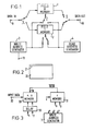
- the special effects equipment comprises two field memories, a field zero memory 1 and a field one memory 2, together with a write address generator 3 and a read address generator 4. These elements are interconnected by switches 5, 6, 7 and 8, each of which is operated at the field frequency. Input data supplied to an input terminal 9 are selectively supplied by way of the switch 5 to the field zero memory 1 or the field one memory 2. Output data for supply to an output terminal 1 are selectively derived by the switch 6 from the field zero memory 1 or the field one memory 2. The write address generator 3 and the read address generator 4 are selectively and alternately connected to the field zero memory 1 and the field one memory 2 by the switches 7 and 8.
- an input analog signal is sampled 2048 times per horizontal scan line and the resulting sample values are pulse code modulation coded into 8-bit words to form the input digital data which are supplied to the input terminal 9.
- Writing proceeds alternately in the field zero memory 1 and the field one memory 2 in dependence on the position of the switch 5 and under the control of the write address generator 3.
- the necessary complex address calculations which are required so as not only to achieve simple writing and reading of the individual digital signals into and out of the appropriate memory 1 or 2, but also to modify the positions of the individual digital signals in a cathode ray tube screen or other video display raster so as to achieve the required special effect, are achieved under the control of a signal supplied to the write address generator 3 by way of an input terminal 11.
- the present invention is particularly concerned with the problem of writing the digital signals in the memories 1 and 2 when the special effect necessitates consideration of the z-dimension position of the data, and in particular where elimination of hidden surfaces is required. This problem will be better understood by consideration of Figure 2.
- Figure 2 indicates the screen 20 of a television receiver on which a straight horizontal line 21, assumed to correspond in position with a horizontal scan line of the receiver is displayed.
- the line 21 is folded back on itself while remaining in the same horizontal plane, so that the right-hand end of the line appears to move perpendicularly away from the screen 20 towards the viewer and backwards in the horizontal direction towards the left-hand end of the line 21. It will be realised that as this movement proceeds, data relating to sample points at the right-hand end of the line 21 will need to over-write data earlier supplied to the memories 1 or 2 and relating to sample points positioned more to the left in the line 21, because those data relate to a surface which is becoming hidden.
- each of the memories 1 and 2 comprises a Y,U/V memory 30 and a z memory 31, although as explained below the z memory 31 is preferably common to the memories 1 and 2.
- the Y,U/V memory 30, hereinafter referred to as the x/y memory 30, stores the 8-bit words forming the pulse code modulated luminance and chrominance sample data, according to the two-dimensional or x and y positions of the individual samples, that is, according to the raster position of the sample in the plane of the television screen.
- the x/y memory 30 is required to store data relating to 2048 samples for each of approximately 520 active scan lines. It is emphasised that the data stored in the x/y memory 30 is information data relating to the actual values of the samples.
- the z memory 31 stores 8-bit words representing the z-dimension position, or depth information, for each of the luminance and chrominance sample data stored in the x/y memory 30, and, as in the x/y memory 30, this data is stored according to the two-dimensional x and y positions of the individual samples. It is, however, emphasised that the data stored in the z memory 31 merely relates to the position of the sample in the z-dimension and not to the actual value of the sample.
- the words stored in the z memory 31 may be 8-bit words, but this is not essential, and words of shorter or longer length can be used depending on the accuracy with which it is required to resolve the positions of two samples which are closely adjacent to one another in the z-dimension.
- the write address generator 3 generates x, y and z address signals in dependence on the special effect required.
- the x and y address signals are supplied to the x/y memory 30 and the x, y and z address signals are supplied to the z memory 31.
- the input 8-bit data words supplied by way of an input 32 to the x/y memory 30 are stored or not stored therein in dependence on a write enable signal WEN generated by a comparator circuit associated with the z memory 31. This comparison is carried out before writing because the data written in the x/y store memory 30 relates to the output field to be read from the x/y store memory 30, and hence hidden surface data is not written therein.
- the comparator circuit checks the data held in the z memory 31 in respect of that sample position with the z data corresponding to the input data word, and the input data word is only written in the x/y memory 30 if the z data indicates that it is nearer to the viewing plane than any data already written in the x/y memory 30 and corresponding to that sample position.
- all the x/y locations in the z memory 31 are set to a zero datum level during the vertical blanking interval preceding each field. This zero datum level is chosen to correspond to the value of z corresponding to the furthest distance from the viewing plane.
- the z memory 31 can be common to the memories 1 and 2 as indicated above. Because the comparator circuit requires some time to effect the comparison, the x and y address signals are supplied to the x/y memory 30 by way of a delay circuit 33, or alternatively are latched so as to be available if and when the write enable signal WEN is supplied.
- the x and y address signals, and also the z address signals, which for convenience will hereinafter be referred to as the z data, are supplied in common over a vertical bus 40 to a buffer circuit 41 or over a horizontal bus 42 to a buffer circuit 43.
- the arrangement is such that data relating to eight sample positions can be handled simultaneously as described in more detail in our copending European patent applications nos. 85306503.5 and 85306504.3, but as this precise arrangement is not of great relevance to the present invention, it will not be further described here. It is sufficient to say that the effect is that this simultaneous supply of data results in the required speed of operation being cut by a factor of eight, but even so in the television system referred to above it is still necessary to complete each comparison within a cycle time of 114 nanoseconds.
- VBUSEN and HBUSEN are respectively supplied to the buffer circuits 41 and 43, and the outputs of the buffer circuits 41 and 43 are connected in common to a latch circuit 44, a latch circuit 45 and a comparator circuit 46.
- a chip enable signal CE and an address clock ADDRCLK are supplied to the latch circuit 44, which supplies outputs to an enable input and the address input of a random access memory (RAM) which forms the z memory 31.
- the latch circuit 45 supplies an output to the data input of the z memory 31, while a data output of the z memory 31 is connected to a second input of the comparator circuit 46.
- a data latch enable signal DLE is supplied to the latch circuit 45 and to the comparator circuit 46, while the write enable signal WEN is developed by the comparator circuit 46 and supplied to the x/y memory 30 ( Figure 3) and also to one input of an OR-circuit 47.
- To a second input of the OR-circuit 47 is supplied a write pulse WR and the output of the OR-circuit 47 is supplied to the write input of the z memory 31.
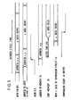
- Figure 5 is a time chart indicating rather more than one memory cycle time of 114 nanoseconds.
- one of the buffer circuits 41 or 43 will supply the x and y address signals which will be latched in the latch circuit 44.
- the z data or more accurately the new z data relating to that sample position, is supplied by the buffer circuit 41 or 43 and is held in the latch circuit 45 and is also latched at the P input of the comparator circuit 46.
- the latch circuit 44 On receipt of the next address clock ADDRCLK the latch circuit 44 supplies the x and y address signals to the z memory 31 which, after an access time, taken to be 35 nanoseconds, supplies the old z data stored at that address to the Q-input of the comparator circuit 46 where it is likewise latched. The new and the old z data are then compared by the comparator circuit 46.
- the comparator circuit 46 supplies the write enable signal WEN.
- Receipt of the write enable signal WEN by the x/y memory 30 causes the input sample data relating to that x/y position to be written (or over-written) in the appropriate position in the x/y memory 30. Additionally, however, if the write enable signal WEN is present on the first input of the OR-circuit 47 at the time of the write pulse WR, then the write pulse WR is supplied to the write input of the z memory 31 and the new z data is over-written at the appropriate x/y position in the z address 31.
Landscapes
- Engineering & Computer Science (AREA)
- Physics & Mathematics (AREA)
- General Physics & Mathematics (AREA)
- Signal Processing (AREA)
- Geometry (AREA)
- Computer Graphics (AREA)
- Multimedia (AREA)
- Theoretical Computer Science (AREA)
- Studio Circuits (AREA)
- Picture Signal Circuits (AREA)
- Processing Of Color Television Signals (AREA)
- Image Processing (AREA)
- Television Systems (AREA)
Priority Applications (1)
| Application Number | Priority Date | Filing Date | Title |
|---|---|---|---|
| AT85307536T ATE55528T1 (de) | 1984-10-31 | 1985-10-18 | Videosignalverarbeitungskreise. |
Applications Claiming Priority (2)
| Application Number | Priority Date | Filing Date | Title |
|---|---|---|---|
| GB8427479 | 1984-10-31 | ||
| GB08427479A GB2166316B (en) | 1984-10-31 | 1984-10-31 | Video signal processing circuits |
Publications (2)
| Publication Number | Publication Date |
|---|---|
| EP0180385A1 true EP0180385A1 (de) | 1986-05-07 |
| EP0180385B1 EP0180385B1 (de) | 1990-08-08 |
Family
ID=10569008
Family Applications (1)
| Application Number | Title | Priority Date | Filing Date |
|---|---|---|---|
| EP85307536A Expired - Lifetime EP0180385B1 (de) | 1984-10-31 | 1985-10-18 | Videosignalverarbeitungskreise |
Country Status (7)
| Country | Link |
|---|---|
| US (1) | US4689677A (de) |
| EP (1) | EP0180385B1 (de) |
| JP (1) | JPH0797842B2 (de) |
| AT (1) | ATE55528T1 (de) |
| CA (1) | CA1251553A (de) |
| DE (1) | DE3579103D1 (de) |
| GB (1) | GB2166316B (de) |
Cited By (4)
| Publication number | Priority date | Publication date | Assignee | Title |
|---|---|---|---|---|
| GB2176676B (en) * | 1985-06-13 | 1989-07-05 | Sun Microsystems Inc | High speed z-buffer with dynamic random access memory |
| EP0307019A3 (en) * | 1987-08-07 | 1990-02-07 | Philips Electronic And Associated Industries Limited | Apparatus for modifying pixel data stored in a random access memory |
| WO1990003703A1 (en) * | 1988-09-22 | 1990-04-05 | Questech Limited | Improvements in and relating to the production of digital video effects |
| GB2228850A (en) * | 1988-12-29 | 1990-09-05 | Daikin Ind Ltd | Hidden surface removal using depth data |
Families Citing this family (6)
| Publication number | Priority date | Publication date | Assignee | Title |
|---|---|---|---|---|
| GB2181929B (en) * | 1985-10-21 | 1989-09-20 | Sony Corp | Methods of and apparatus for video signal processing |
| US5038297A (en) * | 1988-09-13 | 1991-08-06 | Silicon Graphics, Inc. | Method and apparatus for clearing a region of Z-buffer |
| DE68925651T2 (de) * | 1988-09-13 | 1996-09-26 | Silicon Graphics Inc | Verfahren und vorrichtung zum auslöschen eines gebietes eines z-puffers |
| US4947257A (en) * | 1988-10-04 | 1990-08-07 | Bell Communications Research, Inc. | Raster assembly processor |
| US6314485B1 (en) * | 1997-11-14 | 2001-11-06 | Agere Systems Guardian Corp. | Automatic status register |
| US10296088B2 (en) * | 2016-01-26 | 2019-05-21 | Futurewei Technologies, Inc. | Haptic correlated graphic effects |
Citations (2)
| Publication number | Priority date | Publication date | Assignee | Title |
|---|---|---|---|---|
| US4222048A (en) * | 1978-06-02 | 1980-09-09 | The Boeing Company | Three dimension graphic generator for displays with hidden lines |
| US4475104A (en) * | 1983-01-17 | 1984-10-02 | Lexidata Corporation | Three-dimensional display system |
Family Cites Families (3)
| Publication number | Priority date | Publication date | Assignee | Title |
|---|---|---|---|---|
| US4317114A (en) * | 1980-05-12 | 1982-02-23 | Cromemco Inc. | Composite display device for combining image data and method |
| US4439760A (en) * | 1981-05-19 | 1984-03-27 | Bell Telephone Laboratories, Incorporated | Method and apparatus for compiling three-dimensional digital image information |
| US4697178A (en) * | 1984-06-29 | 1987-09-29 | Megatek Corporation | Computer graphics system for real-time calculation and display of the perspective view of three-dimensional scenes |
-
1984
- 1984-10-31 GB GB08427479A patent/GB2166316B/en not_active Expired
-
1985
- 1985-10-02 US US06/783,116 patent/US4689677A/en not_active Expired - Lifetime
- 1985-10-08 CA CA000492457A patent/CA1251553A/en not_active Expired
- 1985-10-18 EP EP85307536A patent/EP0180385B1/de not_active Expired - Lifetime
- 1985-10-18 DE DE8585307536T patent/DE3579103D1/de not_active Expired - Lifetime
- 1985-10-18 AT AT85307536T patent/ATE55528T1/de not_active IP Right Cessation
- 1985-10-31 JP JP60244582A patent/JPH0797842B2/ja not_active Expired - Fee Related
Patent Citations (2)
| Publication number | Priority date | Publication date | Assignee | Title |
|---|---|---|---|---|
| US4222048A (en) * | 1978-06-02 | 1980-09-09 | The Boeing Company | Three dimension graphic generator for displays with hidden lines |
| US4475104A (en) * | 1983-01-17 | 1984-10-02 | Lexidata Corporation | Three-dimensional display system |
Cited By (5)
| Publication number | Priority date | Publication date | Assignee | Title |
|---|---|---|---|---|
| GB2176676B (en) * | 1985-06-13 | 1989-07-05 | Sun Microsystems Inc | High speed z-buffer with dynamic random access memory |
| EP0307019A3 (en) * | 1987-08-07 | 1990-02-07 | Philips Electronic And Associated Industries Limited | Apparatus for modifying pixel data stored in a random access memory |
| WO1990003703A1 (en) * | 1988-09-22 | 1990-04-05 | Questech Limited | Improvements in and relating to the production of digital video effects |
| GB2228850A (en) * | 1988-12-29 | 1990-09-05 | Daikin Ind Ltd | Hidden surface removal using depth data |
| GB2228850B (en) * | 1988-12-29 | 1993-08-18 | Daikin Ind Ltd | Method and apparatus for generating an image representing a three dimensional object |
Also Published As
| Publication number | Publication date |
|---|---|
| GB2166316B (en) | 1987-10-28 |
| JPH0797842B2 (ja) | 1995-10-18 |
| JPS61116474A (ja) | 1986-06-03 |
| ATE55528T1 (de) | 1990-08-15 |
| EP0180385B1 (de) | 1990-08-08 |
| CA1251553A (en) | 1989-03-21 |
| GB8427479D0 (en) | 1984-12-05 |
| DE3579103D1 (de) | 1990-09-13 |
| GB2166316A (en) | 1986-04-30 |
| US4689677A (en) | 1987-08-25 |
Similar Documents
| Publication | Publication Date | Title |
|---|---|---|
| US4953107A (en) | Video signal processing | |
| US5644364A (en) | Media pipeline with multichannel video processing and playback | |
| US5227863A (en) | Programmable digital video processing system | |
| US6509931B1 (en) | Resolution conversion unit and apparatus having resolution conversion unit | |
| US4878117A (en) | Video signal mixing unit for simultaneously displaying video signals having different picture aspect ratios and resolutions | |
| US4783698A (en) | Interpolator for compressed video data | |
| US4689677A (en) | Video signal processing circuits | |
| US5469228A (en) | Memory address and display control apparatus for high definition television | |
| US4757384A (en) | Video signal processing systems | |
| US5121210A (en) | Video composing system using special effect apparatus | |
| US4689681A (en) | Television special effects system | |
| US5327501A (en) | Apparatus for image transformation | |
| KR100451584B1 (ko) | 웨이블릿 변환과 움직임 추정을 이용한 동영상 부호화 및복호화 장치 | |
| US5081449A (en) | Method and apparatus for displaying image information | |
| EP0068882B1 (de) | Kathodenstrahlanzeigeeinrichtung mit einer Schaltung zur Wiederordnung des Bildes | |
| US5963221A (en) | Device for writing and reading of size reduced video on a video screen by fixing read and write of alternating field memories during resize operation | |
| EP0122094B1 (de) | Elektronischer Einzelbildspeicher mit Schnellsortierung und Verfahren zu seinem Betrieb | |
| US5023720A (en) | Single channel video push effect | |
| US4918530A (en) | Processing of video image signals | |
| US5500682A (en) | Memory equipment for writing/reading a defective video signal in a FIFO memory device consectively | |
| JP2006141042A (ja) | マルチチャネル映像処理および再生を備えたメディア・パイプライン | |
| US4511892A (en) | Variable refresh rate for stroke CRT displays | |
| US4633312A (en) | Interframe encoding system having a buffer simulator | |
| US4689682A (en) | Method and apparatus for carrying out television special effects | |
| US4766496A (en) | Video signal memories |
Legal Events
| Date | Code | Title | Description |
|---|---|---|---|
| PUAI | Public reference made under article 153(3) epc to a published international application that has entered the european phase |
Free format text: ORIGINAL CODE: 0009012 |
|
| AK | Designated contracting states |
Kind code of ref document: A1 Designated state(s): AT DE FR GB NL |
|
| 17P | Request for examination filed |
Effective date: 19860924 |
|
| 17Q | First examination report despatched |
Effective date: 19890530 |
|
| GRAA | (expected) grant |
Free format text: ORIGINAL CODE: 0009210 |
|
| AK | Designated contracting states |
Kind code of ref document: B1 Designated state(s): AT DE FR GB NL |
|
| REF | Corresponds to: |
Ref document number: 55528 Country of ref document: AT Date of ref document: 19900815 Kind code of ref document: T |
|
| REF | Corresponds to: |
Ref document number: 3579103 Country of ref document: DE Date of ref document: 19900913 |
|
| ET | Fr: translation filed | ||
| PLBE | No opposition filed within time limit |
Free format text: ORIGINAL CODE: 0009261 |
|
| STAA | Information on the status of an ep patent application or granted ep patent |
Free format text: STATUS: NO OPPOSITION FILED WITHIN TIME LIMIT |
|
| 26N | No opposition filed | ||
| REG | Reference to a national code |
Ref country code: GB Ref legal event code: IF02 |
|
| PGFP | Annual fee paid to national office [announced via postgrant information from national office to epo] |
Ref country code: NL Payment date: 20041003 Year of fee payment: 20 |
|
| PGFP | Annual fee paid to national office [announced via postgrant information from national office to epo] |
Ref country code: FR Payment date: 20041008 Year of fee payment: 20 |
|
| PGFP | Annual fee paid to national office [announced via postgrant information from national office to epo] |
Ref country code: GB Payment date: 20041013 Year of fee payment: 20 Ref country code: AT Payment date: 20041013 Year of fee payment: 20 |
|
| PGFP | Annual fee paid to national office [announced via postgrant information from national office to epo] |
Ref country code: DE Payment date: 20041014 Year of fee payment: 20 |
|
| PG25 | Lapsed in a contracting state [announced via postgrant information from national office to epo] |
Ref country code: GB Free format text: LAPSE BECAUSE OF EXPIRATION OF PROTECTION Effective date: 20051017 |
|
| PG25 | Lapsed in a contracting state [announced via postgrant information from national office to epo] |
Ref country code: NL Free format text: LAPSE BECAUSE OF EXPIRATION OF PROTECTION Effective date: 20051018 |
|
| REG | Reference to a national code |
Ref country code: GB Ref legal event code: PE20 |
|
| NLV7 | Nl: ceased due to reaching the maximum lifetime of a patent |
Effective date: 20051018 |